 | –≠–ª–µ–∫—Ç—Ä–æ–Ω–Ω—ã–π –∫–æ–º–ø–æ–Ω–µ–Ω—Ç: TSL261R | –°–∫–∞—á–∞—Ç—å:  PDF PDF  ZIP ZIP |

TSL260R, TSL261R, TSL262R
INFRARED LIGHT TO VOLTAGE OPTICAL SENSORS
TAOS049 ≠ JANUARY 2003
1
The
LUMENOLOGY
r
Company
t
t
Copyright
E
2003, TAOS Inc.
www.taosinc.com
D
Integral Visible Light Cutoff Filter
D
Monolithic Silicon IC Containing
Photodiode, Operational Amplifier, and
Feedback Components
D
Converts Light Intensity to a Voltage
D
High Irradiance Responsivity, Typically
111 mV/(
m
W/cm
2
) at
l
p
= 940 nm (TSL260R)
D
Compact 3-Lead Plastic Package
D
Single Voltage Supply Operation
D
Low Dark (Offset) Voltage....10mV Max
D
Low Supply Current......1.1 mA Typical
D
Wide Supply-Voltage Range.... 2.7 V to 5.5 V
D
Replacements for TSL260, TSL261, and
TSL262
Description
The TSL260R, TSL261R, and TSL262R are infrared light-to-voltage optical sensors, each combining a
photodiode and a transimpedance amplifier (feedback resistor = 16 M
, 8 M
, and 2.8 M
respectively) on a
single monolithic IC. Output voltage is directly proportional to the light intensity (irradiance) on the photodiode.
These devices have improved amplifier offset-voltage stability and low power consumption and are supplied
in a 3-lead plastic sidelooker package with an integral visible light cutoff filter and lens.
Functional Block Diagram
Voltage
Output
+
≠
Terminal Functions
TERMINAL
DESCRIPTION
NAME
NO.
DESCRIPTION
GND
1
Ground (substrate). All voltages are referenced to GND.
OUT
3
Output voltage
V
DD
2
Supply voltage
t
t
Texas Advanced Optoelectronic Solutions Inc.
800 Jupiter Road, Suite 205
S
Plano, TX 75074
S
(972) 673-0759
3
2
1
OUT
V
DD
GND
PACKAGE
(FRONT VIEW)

TSL260R, TSL261R, TSL262R
INFRARED LIGHT TO VOLTAGE OPTICAL SENSORS
TAOS049 ≠ JANUARY 2003
2
t
t
Copyright
E
2003, TAOS Inc.
The
LUMENOLOGY
r
Company
www.taosinc.com
Absolute Maximum Ratings over operating free-air temperature range (unless otherwise noted)
Supply voltage, V
DD
(see Note 1)
6 V
. . . . . . . . . . . . . . . . . . . . . . . . . . . . . . . . . . . . . . . . . . . . . . . . . . . . . . . . . . . . .
Output current, I
O
±
10 mA
. . . . . . . . . . . . . . . . . . . . . . . . . . . . . . . . . . . . . . . . . . . . . . . . . . . . . . . . . . . . . . . . . . . . . .
Duration of short-circuit current at (or below) 25
∞
C (see Note 2)
5 s
. . . . . . . . . . . . . . . . . . . . . . . . . . . . . . . . . . .
Operating free-air temperature range, T
A
≠25
∞
C to 85
∞
C
. . . . . . . . . . . . . . . . . . . . . . . . . . . . . . . . . . . . . . . . . . . .
Storage temperature range, T
stg
≠25
∞
C to 85
∞
C
. . . . . . . . . . . . . . . . . . . . . . . . . . . . . . . . . . . . . . . . . . . . . . . . . . . .
Lead temperature 1,6 mm (1/16 inch) from case for 10 seconds
240
∞
C
. . . . . . . . . . . . . . . . . . . . . . . . . . . . . . .
Stresses beyond those listed under "absolute maximum ratings" may cause permanent damage to the device. These are stress ratings only, and
functional operation of the device at these or any other conditions beyond those indicated under "recommended operating conditions" is not
implied. Exposure to absolute-maximum-rated conditions for extended periods may affect device reliability.
NOTES: 1. All voltages are with respect to GND.
2. Output may be shorted to supply.
Recommended Operating Conditions
MIN
NOM
MAX
UNIT
Supply voltage, V
DD
2.7
5.5
V
Operating free-air temperature, T
A
0
70
∞
C
Electrical Characteristics at V
DD
= 5 V, T
A
= 25
∞
C,
p = 940 nm, R
L
= 10 k
(unless otherwise noted)
(see Notes 3, 4, and 5)
PARAMETER
TEST
TSL260R
TSL261R
TSL262R
UNIT
PARAMETER
TEST
CONDITIONS
MIN
TYP
MAX
MIN
TYP
MAX
MIN
TYP
MAX
UNIT
V
D
Dark voltage
E
e
= 0
0
4
10
0
4
10
0
4
10
mV
V
OM
Maximum output
voltage
V
DD
= 4.5 V
3
3.3
3
3.3
3
3.3
V
E
e
= 18
µ
W/cm
2
1
2
3
V
O
Output voltage
E
e
= 46
µ
W/cm
2
1
2
3
V
V
O
Out ut voltage
E
e
= 220
µ
W/cm
2
1
2
3
V
E
e
= 18
µ
W/cm
2
,
8
mV/
∞
C
Temperature
E
e
= 18
µ
W/cm ,
T
A
= 0
∞
C to 70
∞
C
0.4
%/
∞
C
Temperature
coefficient of
E
e
= 46
µ
W/cm
2
,
8
mV/
∞
C
vo
coefficient of
output voltage
(V )
E
e
= 46
µ
W/cm ,
T
A
= 0
∞
C to 70
∞
C
0.4
%/
∞
C
g
(V
O
)
E
e
= 220
µ
W/cm
2
,
8
mV/
∞
C
E
e
= 220
µ
W/cm ,
T
A
= 0
∞
C to 70
∞
C
0.4
%/
∞
C
N
e
Irradiance
responsivity
See Note 6
111
43.5
9.1
mV/(
µ
W/cm
2
)
E
e
= 18
µ
W/cm
2
1.1
1.7
I
DD
Supply current
E
e
= 46
µ
W/cm
2
1.1
1.7
mA
DD
y
E
e
= 220
µ
W/cm
2
1.1
1.7
NOTES: 3. Measurements are made with R
L
= 10 k
between output and ground.
4. Optical measurements are made using small-angle incident radiation from an LED optical source.
5. The input irradiance E
e
is supplied by a GaAs LED with peak wavelength
p
= 940 nm
6. Irradiance responsivity is characterized over the range V
O
= 0.05 to 2.9 V. The best-fit straight line of Output Voltage V
O
versus
irradiance E
e
over this range will typically have a positive extrapolated V
O
value for E
e
= 0.
TSL260R, TSL261R, TSL262R
INFRARED LIGHT TO VOLTAGE OPTICAL SENSORS
TAOS049 ≠ JANUARY 2003
3
The
LUMENOLOGY
r
Company
t
t
Copyright
E
2003, TAOS Inc.
www.taosinc.com
Dynamic Characteristics at T
A
= 25
∞
C (see Figure 1)
PARAMETER
TEST CONDITIONS
TSL260R
TSL261R
TSL262R
UNIT
PARAMETER
TEST CONDITIONS
MIN
TYP
MAX
MIN
TYP
MAX
MIN
TYP
MAX
UNIT
t
r
Output pulse rise time
V
DD
= 5 V,
p
= 940 nm
260
70
7
µ
s
t
f
Output pulse fall time
V
DD
= 5 V,
p
= 940 nm
260
70
7
µ
s
V
n
Output noise voltage
V
DD
= 5 V,
f = 1000 Hz
E
e
= 0,
0.8
0.7
0.6
µ
V/
Hz
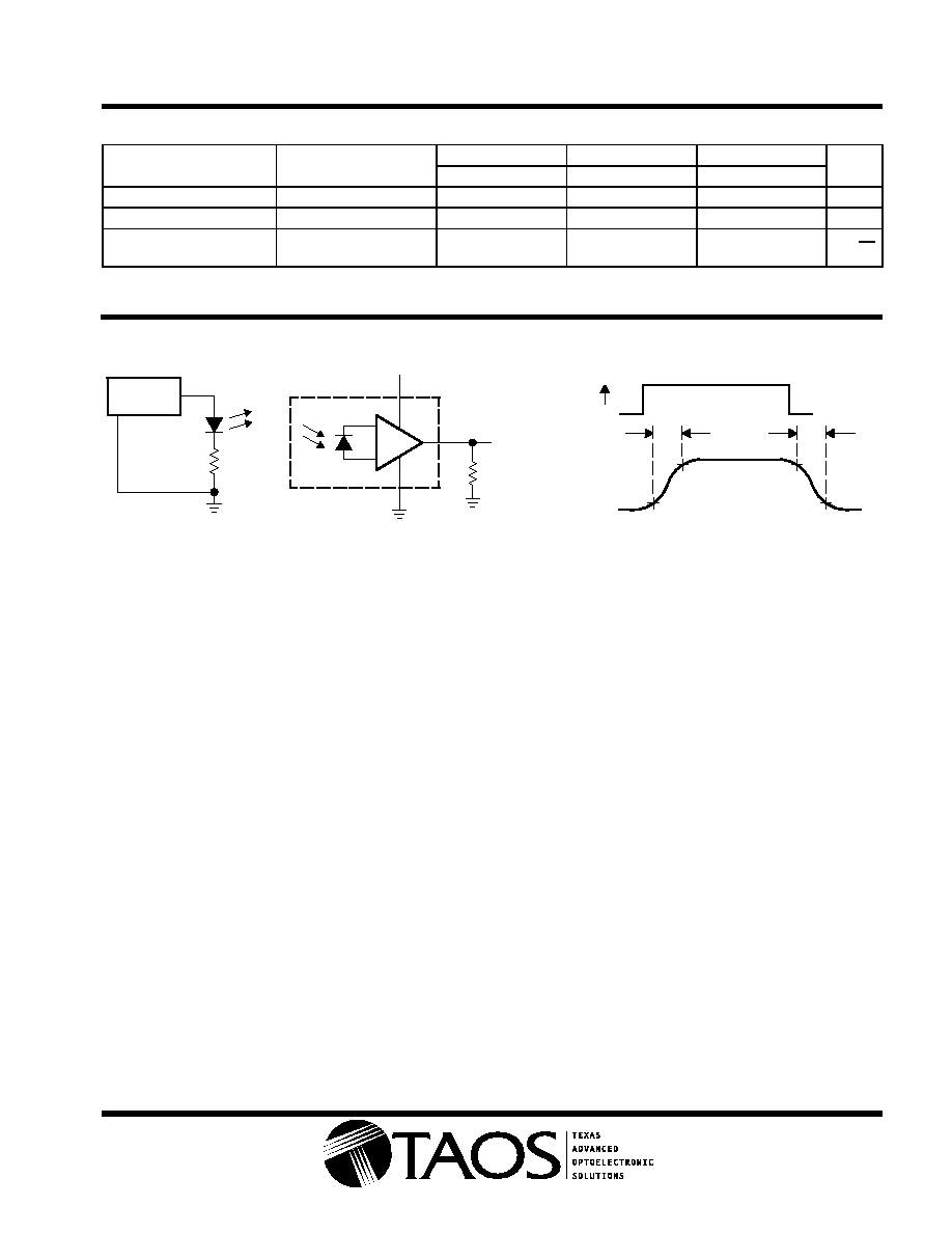
PARAMETER MEASUREMENT INFORMATION
VOLTAGE WAVEFORM
TEST CIRCUIT
Input
E
e
10%
90%
Output
(see Note B)
t
r
TSL26xR
R
L
V
DD
2
1
3
+
≠
Output
Pulse
Generator
LED
(see Note A)
t
f
90%
10%
NOTES: A. The input irradiance is supplied by a pulsed GaAs light-emitting diode with the following characteristics:
p
= 940 nm,
t
r
< 1
µ
s, t
f
< 1
µ
s.
B. The output waveform is monitored on an oscilloscope with the following characteristics: t
r
< 100 ns, Z
i
1 M
, C
i
20 pF.
Figure 1. Switching Times

TSL260R, TSL261R, TSL262R
INFRARED LIGHT TO VOLTAGE OPTICAL SENSORS
TAOS049 ≠ JANUARY 2003
4
t
t
Copyright
E
2003, TAOS Inc.
The
LUMENOLOGY
r
Company
www.taosinc.com
TYPICAL CHARACTERISTICS
OUTPUT VOLTAGE
vs
IRRADIANCE
Figure 2
0.1
1
10
100
1000
V
DD
= 5 V
p
= 940 nm
R
L
= 10 k
W
T
A
= 25
∞
C
V
O
-- Output V
oltage -- V
E
e
-- Irradiance --
m
W/cm
2
0.01
0.1
1
10
TSL260R
TSL261R
TSL262R
Figure 3
PHOTODIODE SPECTRAL RESPONSIVITY
≠ Wavelength ≠ nm
700
800
900
1000
1100
600
0
0.2
0.4
0.6
0.8
1
Relative Responsivity
T
A
= 25
∞
C
Figure 4
4
2
1
0
5.5
2.5
3
3.5
5
MAXIMUM OUTPUT VOLTAGE
vs
SUPPLY VOLTAGE
4
4.5
5
≠ Maximum Output V
oltage
≠
V
V
OM
3
V
DD
≠ Supply Voltage ≠ V
R
L
= 10 k
T
A
= 25
∞
C
Figure 5
1
0.6
0
1
2
3
1.6
4
1.4
1.2
0.8
V
O
≠ Output Voltage ≠ V
≠ Supply Current ≠ mA
I DD
SUPPLY CURRENT
vs
OUTPUT VOLTAGE
V
DD
= 5 V
R
L
= 10 k
W
T
A
= 25
∞
C

TSL260R, TSL261R, TSL262R
INFRARED LIGHT TO VOLTAGE OPTICAL SENSORS
TAOS049 ≠ JANUARY 2003
5
The
LUMENOLOGY
r
Company
t
t
Copyright
E
2003, TAOS Inc.
www.taosinc.com
TYPICAL CHARACTERISTICS
0.4
0
Normalized Output V
oltage
1
0.8
0.6
0.2
≠ Angular Displacement
TSL260R
80
∞
60
∞
40
∞
20
∞
0
∞
80
∞
60
∞
40
∞
20
∞
Optical Axis
NORMALIZED OUTPUT VOLTAGE
vs
ANGULAR DISPLACEMENT
V
≠ O
Figure 6
TSL262R
TSL261R