 | –≠–ª–µ–∫—Ç—Ä–æ–Ω–Ω—ã–π –∫–æ–º–ø–æ–Ω–µ–Ω—Ç: TSLB257 | –°–∫–∞—á–∞—Ç—å:  PDF PDF  ZIP ZIP |
TSLB257, TSLG257, TSLR257
HIGH SENSITIVITY COLOR
LIGHT TO VOLTAGE CONVERTERS
TAOS027B ≠ MARCH 2002
1
The
LUMENOLOGY
r
Company
t
t
Copyright
E
2002, TAOS Inc.
www.taosinc.com
D
Converts Light Intensity to Output Voltage
D
Integral Color Filter in Blue, Green, or Red
D
Monolithic Silicon IC Containing
Photodiode, Operational Amplifier, and
Feedback Components
D
High Sensitivity
D
Single Voltage Supply Operation
D
Low Noise (200
µ
Vrms Typ to 1 kHz)
D
Rail-to-Rail Output
D
High Power-Supply Rejection (35 dB at
1 kHz)
D
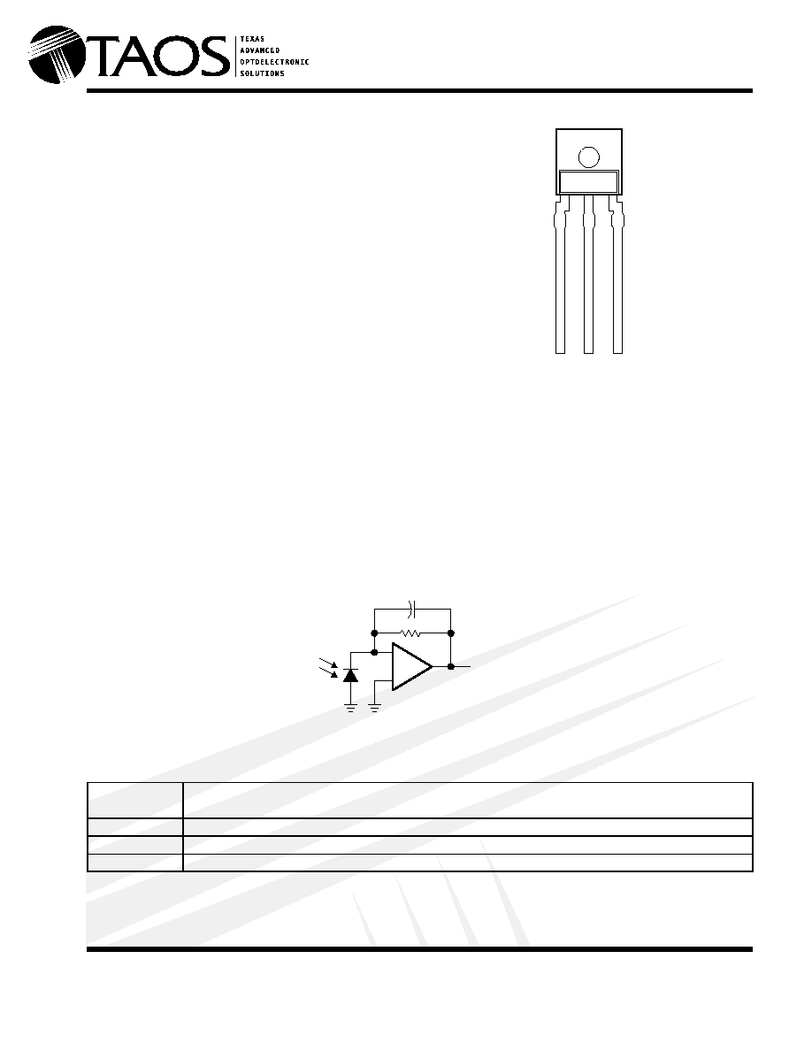
Compact 3-Leaded Plastic Package
Description
The TSLB257, TSLG257, and TSLR257 are high-sensitivity low-noise light-to-voltage optical converters that
incorporate onboard blue, green, and red optical filters, respectively. These devices combine a photodiode and
a transimpedance amplifier on a single monolithic CMOS integrated circuit with a color filter over the photodiode.
Output voltage is directly proportional to light intensity (irradiance) on the photodiode. Each device has a
transimpedance gain of 320 M
with improved
offset voltage stability and low power consumption, and is
supplied in a 3-lead clear plastic sidelooker package with an integral lens.
These devices are ideal for applications such as colorimetry, printing process control, display color correction,
and selectively ambient light detection or rejection.
Functional Block Diagram
Voltage
Output
+
≠
Terminal Functions
TERMINAL
DESCRIPTION
NAME
NO.
DESCRIPTION
GND
1
Ground (substrate). All voltages are referenced to GND.
OUT
3
Output voltage
V
DD
2
Supply voltage
t
t
Texas Advanced Optoelectronic Solutions Inc.
800 Jupiter Road, Suite 205
S
Plano, TX 75074
S
(972) 673-0759
3
2
1
OUT
V
DD
GND
PACKAGE
(FRONT VIEW)
TSLB257, TSLG257, TSLR257
HIGH SENSITIVITY COLOR
LIGHT TO VOLTAGE CONVERTERS
TAOS027B ≠ MARCH 2002
2
t
t
Copyright
E
2002, TAOS Inc.
The
LUMENOLOGY
r
Company
www.taosinc.com
Absolute Maximum Ratings over operating free-air temperature range (unless otherwise noted)
Supply voltage, V
DD
(see Note 1)
6 V
. . . . . . . . . . . . . . . . . . . . . . . . . . . . . . . . . . . . . . . . . . . . . . . . . . . . . . . . . . . . .
Output current, I
O
±
10 mA
. . . . . . . . . . . . . . . . . . . . . . . . . . . . . . . . . . . . . . . . . . . . . . . . . . . . . . . . . . . . . . . . . . . . . .
Duration of short-circuit current at (or below) 25
∞
C
5 s
. . . . . . . . . . . . . . . . . . . . . . . . . . . . . . . . . . . . . . . . . . . . . .
Operating free-air temperature range, T
A
≠25
∞
C to 85
∞
C
. . . . . . . . . . . . . . . . . . . . . . . . . . . . . . . . . . . . . . . . . . . .
Storage temperature range, T
stg
≠25
∞
C to 85
∞
C
. . . . . . . . . . . . . . . . . . . . . . . . . . . . . . . . . . . . . . . . . . . . . . . . . . . .
Lead temperature 1,6 mm (1/16 inch) from case for 10 seconds
240
∞
C
. . . . . . . . . . . . . . . . . . . . . . . . . . . . . . .
Stresses beyond those listed under "absolute maximum ratings" may cause permanent damage to the device. These are stress ratings only, and
functional operation of the device at these or any other conditions beyond those indicated under "recommended operating conditions" is not
implied. Exposure to absolute-maximum-rated conditions for extended periods may affect device reliability.
NOTE 1: All voltages are with respect to GND.
Recommended Operating Conditions
MIN
MAX
UNIT
Supply voltage, V
DD
2.7
5.5
V
Operating free-air temperature, T
A
0
70
∞
C
TSLB257, TSLG257, TSLR257
HIGH SENSITIVITY COLOR
LIGHT TO VOLTAGE CONVERTERS
TAOS027B ≠ MARCH 2002
3
The
LUMENOLOGY
r
Company
t
t
Copyright
E
2002, TAOS Inc.
www.taosinc.com
Electrical Characteristics at V
DD
= 5 V, T
A
= 25
∞
C, R
L
= 10 k
(unless otherwise noted) (see Notes
2 and 3)
PARAMETER
TEST CONDITIONS
TSLB257
TSLG257
TSLR257
UNIT
PARAMETER
TEST CONDITIONS
MIN
TYP
MAX
MIN
TYP
MAX
MIN
TYP
MAX
UNIT
V
D
Dark voltage
E
e
= 0
0
15
0
15
0
15
mV
V
Maximum output voltage
V
DD
= 4.5 V, No Load
4.49
4.49
4.49
V
V
OM
Maximum out ut voltage
swing
V
DD
= 4.5 V, R
L
= 10 k
4
4.2
4
4.2
4
4.2
V
E
e
= 1.7
µ
W/cm
2
,
p
= 470 nm, Note 4
1.3
2
2.7
V
O
Output voltage
E
e
= 1.6
µ
W/cm
2
,
p
= 524 nm, Note 5
1.3
2
2.7
V
E
e
= 1.1
µ
W/cm
2
,
p
= 635 nm, Note 6
1.3
2
2.7
VD
Temperature coefficient
of dark voltage (V
D
)
T
A
= 0
∞
C to 70
∞
C
≠15
≠15
≠15
µ
V/
∞
C
p
= 470 nm,
see Notes 4 and 7
1.18
0.35
0.09
R
Irradiance responsivity
p
= 524 nm,
see Notes 5 and 7
0.53
1.25
0.14
V/
(
µ
W/
R
e
Irradiance responsivity
p
=565 nm,
see Notes 7 and 8
0.09
1.17
0.36
(
µ
W/
cm
2
)
p
= 635 nm,
see Notes 6 and 7
0.05
0.14
1.82
p
= 470 nm,
see Notes 4 and 7
1.57
0.47
0.12
R
Illuminance responsivity
p
= 524 nm,
see Notes 5 and 7
0.10
0.24
0.027
V/Ix
R
V
Illuminance responsivity
p
= 565 nm,
see Notes 7 and 8
0.015
0.20
0.06
V/Ix
p
= 635 nm,
see Notes 6 and 7
0.033
0.093
1.21
PSRR
Power supply rejection
f
ac
= 100 Hz, see Note 10
55
55
55
dB
y
j
ratio
f
ac
= 1 kHz, see Note 10
35
35
35
dB
I
DD
Supply current
V
O
= 2 V (typical)
1.9
3.5
1.9
3.5
1.9
3.5
mA
NOTES: 2. Measured with R
L
= 10 k
between output and ground.
3. Optical measurements are made using small-angle incident radiation from a light-emitting diode (LED) optical source.
4. The input irradiance is supplied by an InGaN light-emitting diode with the following characteristics: peak wavelength
p
= 470 nm,
spectral halfwidth
Ω
= 35 nm, luminous efficacy = 75 lm/W.
5. The input irradiance is supplied by an InGaN light-emitting diode with the following characteristics: peak wavelength
p
= 524 nm,
spectral halfwidth
Ω
= 47 nm, luminous efficacy = 520 lm/W.
6. The input irradiance is supplied by an Al
I
nGaP light-emitting diode with the following characteristics: peak wavelength
p
= 635 nm,
spectral halfwidth
Ω
= 17 nm, luminous efficacy = 150 lm/W.
7. Responsivity is characterized over the range V
O
= 0.1 V to 4.5 V. The best-fit straight line of Output Voltage V
O
versus Irradiance
E
e
over this range will typically have a positive extrapolated V
O
value for E
e
= 0.
8. The input irradiance is supplied by a GaP light-emitting diode with the following characteristics: peak wavelength
p
= 565 nm,
spectral halfwidth
Ω
= 28 nm, luminous efficacy = 595 lm/W.
9. Illuminance responsivity R
V
is calculated from the irradiance responsivity by using the LED luminous efficacy values stated in Notes
4, 5, 6, and 8, and using 1 lx = 1 lm/m
2
.
10. Power supply rejection ratio PSRR is defined as 20 log (
V
DD
(f)/
V
O
(f)) with V
DD
(f = 0) = 5 V and V
O
(f = 0) = 2 V.
TSLB257, TSLG257, TSLR257
HIGH SENSITIVITY COLOR
LIGHT TO VOLTAGE CONVERTERS
TAOS027B ≠ MARCH 2002
4
t
t
Copyright
E
2002, TAOS Inc.
The
LUMENOLOGY
r
Company
www.taosinc.com
Switching Characteristics at V
DD
= 5 V, T
A
= 25
∞
C, R
L
= 10 k
(unless otherwise noted)
PARAMETER
TEST CONDITIONS
MIN
TYP
MAX
UNIT
t
r
Output pulse rise time, 10% to 90% of final value
See Note 11 and Figure 1
160
250
µ
s
t
f
Output pulse fall time, 10% to 90% of final value
See Note 11 and Figure 1
150
250
µ
s
t
s
Output settling time to 1% of final value
See Note 11 and Figure 1
330
µ
s
Integrated noise voltage
f = dc to 1 kHz
E
e
= 0
200
µ
Vrms
f = 10 Hz
E
e
= 0
6
V
n
Output noise voltage, rms
f = 100 Hz
E
e
= 0
6
µ
V/
Hz rms
n
g ,
f = 1 kHz
E
e
= 0
7
µ
NOTE 11: Switching characteristics apply over the range V
O
= 0.1 V to 4.5 V.
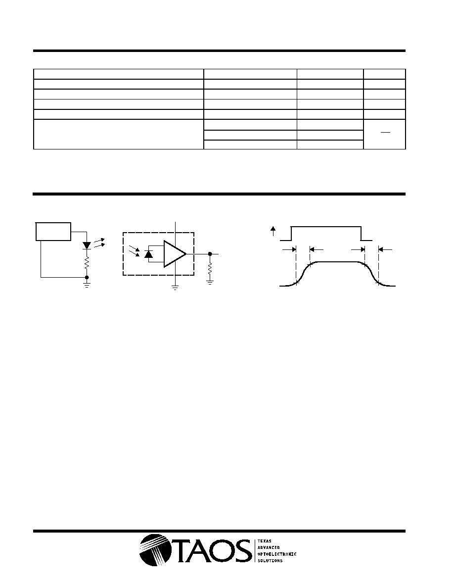
PARAMETER MEASUREMENT INFORMATION
VOLTAGE WAVEFORM
TEST CIRCUIT
Input
E
e
10%
90%
Output
(see Note B)
t
r
TSLx257
R
L
V
DD
2
1
3
+
≠
Output
Pulse
Generator
LED
(see Note A)
t
f
90%
10%
NOTES: A. The input irradiance is supplied by a pulsed light-emitting diode with the following characteristics: t
r
< 1
µ
s, t
f
< 1
µ
s.
B. The output waveform is monitored on an oscilloscope with the following characteristics: t
r
< 100 ns, Z
i
1 M
, C
i
20 pF.
Figure 1. Switching Times
TSLB257, TSLG257, TSLR257
HIGH SENSITIVITY COLOR
LIGHT TO VOLTAGE CONVERTERS
TAOS027B ≠ MARCH 2002
5
The
LUMENOLOGY
r
Company
t
t
Copyright
E
2002, TAOS Inc.
www.taosinc.com
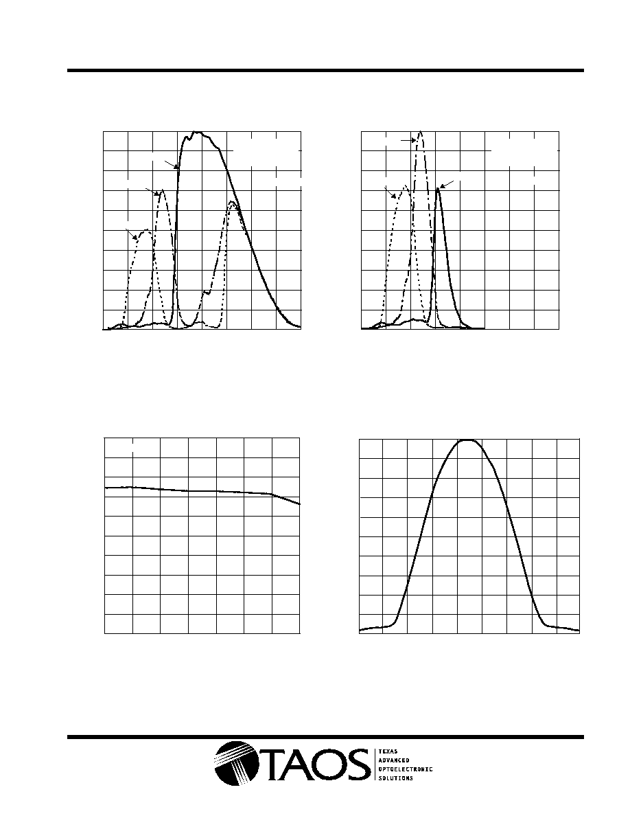
TYPICAL CHARACTERISTICS
Figure 2
300
500
700
900
Relative Responsivity
1100
≠ Wavelength ≠ nm
T
A
= 25
∞
C
PHOTODIODE SPECTRAL RESPONSIVITY
0.1
0.2
0.3
0.4
0.5
0.6
0.7
0.8
0.9
1
0
TSLG257
TSLB257
Normalized to
TSLR257
@ 670 nm
TSLR257
Figure 3
300
500
700
900
Relative Responsivity
1100
≠ Wavelength ≠ nm
T
A
= 25
∞
C
PHOTODIODE SPECTRAL RESPONSIVITY WITH
EXTERNAL HOYA CM500 FILTER
0.1
0.2
0.3
0.4
0.5
0.6
0.7
0.8
0.9
1
0
TSLG257
TSLB257
Normalized to
TSLG257
@ 540 nm
TSLR257
Figure 4
4
2
1
0
70
0
10
DARK VOLTAGE
vs
FREE-AIR TEMPERATURE
10
30
50
≠ Dark V
oltage
≠
mV
V
D
3
T
A
≠ Free-Air Temperature ≠
∞
C
60
20
40
9
7
6
5
8
V
DD
= 5 V
Figure 5
0
NORMALIZED RESPONSE
vs
ANGULAR DISPLACEMENT
≠90
≠70
≠50
≠30
10
30
50
70
90
0.1
0.2
0.3
0.4
0.5
0.6
0.7
0.8
0.9
1.0
Normalized Response
≠10
Angular Displacement ≠
5