 | –≠–ª–µ–∫—Ç—Ä–æ–Ω–Ω—ã–π –∫–æ–º–ø–æ–Ω–µ–Ω—Ç: 73K222BL | –°–∫–∞—á–∞—Ç—å:  PDF PDF  ZIP ZIP |
73K222BL
V.22, V.21, Bell 212A, Bell 103 Single-Chip
Modem with Integrated Hybrid
April 2000
DESCRIPTION
The 73K222BL is a highly integrated single-chip
modem IC which provides the functions needed to
construct a CCITT V.22, V.21, Bell 212A and Bell
103, compatible modem, capable of 1200 bit/s full-
duplex operation over dial-up lines. The 73K222BL
is an enhancement of the 73K222AL single-chip
modem which adds the hybrid hook switch control,
and driver to the 73K222AL. In Bell 212A mode, the
73K222BL provides the normal Bell 212A and Bell
103 functions and employs a 2225 Hz answer tone.
The 73K222BL in V.22 mode produces either 550 or
1800 Hz guard tone, recognizes and generates a
2100 Hz answer tone, and allows 600 bit/s V.22 or
0-300 bit/s V.21 operation. The device integrates
analog, digital, and switched-capacitor array
functions on a single substrate, offering excellent
performance and a high level of functional
integration in a 32-Lead PLCC and 44-Lead TQFP
package. It operates from a single +5 V supply.
The 73K222BL includes the DPSK and FSK
modulator/demodulator functions, call progress and
handshake tone monitor and a tone generator
capable of tones required for European applications.
This device supports V.22 (except mode v) and V. 21
modes of operation, allowing both synchronous and
asynchronous communication. Test features such as
analog loop, digital loop, and remote digital loopback
are supported. Internal pattern generators are also
included for self-testing.
(continued)
FEATURES
∑ Includes features of 73K222AL single-chip
modem
∑ One-chip CCITT V.22, V.21, Bell 212A and Bell
103 standard compatible modem data pump
∑ Full-duplex operation at 0-300 bit/s (FSK) or
600 and 1200 bit/s (DPSK)
∑ On chip 2-wire/4-wire hybrid driver and off-
hook relay buffer driver
∑ Serial or parallel microcontroller control
interface
∑ Interfaces directly with standard
microcontroller (8048, 80C51 typical)
∑ Serial port for data transfer
∑ Both synchronous and asynchronous modes
of operation including V.22 extended
overspeed
∑ Call progress, carrier, precise answer tone
(2100 or 2225 Hz), and long loop detectors
∑ DTMF, and 550 or 1800 Hz guard tone
generators
∑ Test modes available: ALB, DL, RDL, Mark,
Space, Alternating bit patterns
∑ Precise automatic gain control allows 45 dB
dynamic range
∑ CMOS technology for low power consumption
using 60 mW @ 5 V
∑ Single +5 V supply
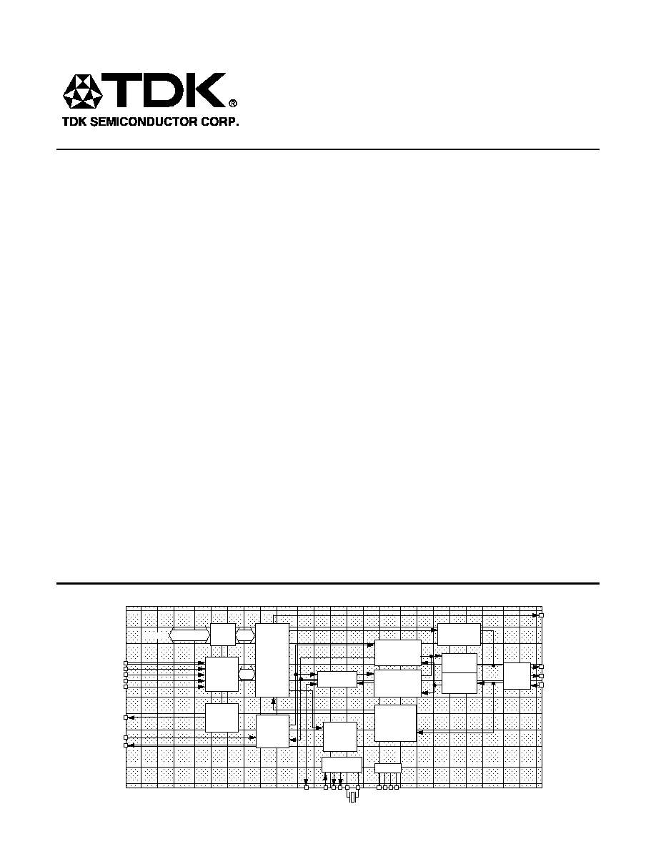
BLOCK DIAGRAM
DIGITAL
PROCESSING
DTMF &
TONE
GENERATORS
FSK
MODULATOR/
DEMODULATOR
PSK
MODULATOR/
DEMODULATOR
SMART
DIALING
&
DETECT
FUNCTIONS
POWER
TESTS:
ALB, DLB
RDLB
PATTERNS
TRANSMIT
FILTER
DATA
BUS
BUFFER
READ
WRITE
CONTROL
LOGIC
STATUS
AND
CONTROL
LOGIC
8-BIT
BUS
FOR
CONTROL
AND
STATUS
SERIAL
PORT
FOR
DATA
TXA1
RXA
ISET
VDD
VREF
GND
RXCLK
CLOCK
GENERATOR
XTL2
XTL1
CLK
TXCLK
EXCLK
RD
WR
ALE
CS
RESET
INT
TXD
RXD
AD0-AD7
RECEIVE
FILTER
2W/4W
HYBRID
TXA2
OH

73K222BL
V.22, V.21, Bell 212A, Bell 103
Single-Chip Modem with Integrated Hybrid
2
DESCRIPTION
(continued)
The 73K222BL is designed to appear to the systems
designer as a microprocessor peripheral, and will
easily interface with popular one-chip
microprocessors (80C51 typical) for control of
modem functions through its 8-bit multiplexed
address/data bus. An ALE control line simplifies
address demultiplexing. Data communications
occurs through a separate serial port only.
The 73K222BL is ideal for use in either free standing
or integral system modem products where full-
duplex 1200 bit/s data communications over the 2-
wire switched telephone network is desired. Its high
functionality, low power consumption and efficient
packaging simplify design requirements and
increase system reliability. A complete modem
requires only the addition of the phone line interface,
a control microprocessor, and RS-232 level
converter for a typical system.
The 73K222BL is part of TDK Semiconductor's
K-Series family of single-chip modem products.
These devices allow systems to be configured for
higher speeds and Bell or CCITT operation with only
a single component change.
FUNCTIONAL DESCRIPTION
HYBRID AND RELAY DRIVER
To make designs more cost effective and space
efficient, the 73K222BL includes the 2-wire to 4-wire
hybrid with sufficient drive to interface directly to the
telecom coupling transformers. In addition, an off
hook relay driver with 40 mA drive capability is also
included to allow use of commonly available
mechanical telecom relays.
ASYNCHRONOUS MODE
Data transmission for the DPSK mode requires that
data ultimately be transmitted in a synchronous
fashion. The 73K222BL includes ASYNC/SYNC and
SYNC/ASYNC converters which delete or insert stop
bits in order to transmit data within a ±0.01% rate. In
asynchronous mode the serial data comes from the
TXD pin into the ASYNC/SYNC converter. The
ASYNC/SYNC converter accepts the data provided
on the TXD pin which normally must be 1200 or 600
bit/s +1.0%, -2.5%. The converter will then insert or
delete stop bits in order to output a signal which is
1200 or 600 bit/s ± 0.01% (± 0.01% is required
synchronous data rate accuracy).
The serial data stream from the ASYNC/SYNC
converter is passed through the data scrambler and
onto the analog modulator. The data scrambler can
be bypassed under processor control when
unscrambled data must be transmitted. The
ASYNC/SYNC converter and the data scrambler are
bypassed in all FSK modes. If serial input data
contains a break signal through one character
(including start and stop bits) the break will be
extended to at least 2
∑ N + 3 bits long (where N is
the number of transmitted bits/character).

73K222BL
V.22, V.21, Bell 212A, Bell 103
Single-Chip Modem with Integrated Hybrid
3
Serial data from the demodulator is passed first
through the data descrambler and then through the
SYNC/ASYNC converter. The SYNC/ASYNC
converter will re-insert any deleted stop bits and
transmit output data at an intra-character rate (bit-to-
bit timing) of no greater than 1219 bit/s. An incoming
break signal (low through two characters) will be
passed through without incorrectly inserting a stop bit.
The SYNC/ASYNC converter also has an extended
overspeed mode which allows selection of an
overspeed range of either +1% or +2.3%. In the
extended overspeed mode, stop bits are output at
7/8 the normal width.
SYNCHRONOUS MODE
The CCITT V.22 standard defines synchronous
operation at 600 and 1200 bit/s. The Bell 212A
standard defines synchronous operation only at
1200 bit/s. Operation is similar to that of the
asynchronous mode except that data must be
synchronized to a provided clock and no variation in
data transfer rate is allowable. Serial input data
appearing at TXD must be valid on the rising edge of
TXCLK.
TXCLK is an internally derived signal in internal
mode and is connected internally to the RXCLK pin
in slave mode. Receive data at the RXD pin is
clocked out on the falling edge of RXCLK. The
ASYNCH/SYNCH converter is bypassed when
synchronous mode is selected and data is
transmitted out at the same rate as it is input.
DPSK MODULATOR/DEMODULATOR
The 73K222BL modulates a serial bit stream into
di-bit pairs that are represented by four possible
phase shifts as prescribed by the Bell 212A or V.22
standards. The baseband signal is then filtered to
reduce intersymbol interference on the bandlimited
2-wire telephone line. Transmission occurs using
either a 1200 Hz (originate mode) or 2400 Hz carrier
(answer mode). Demodulation is the reverse of the
modulation process, with the incoming analog signal
eventually decoded into di-bits and converted back
to a serial bit stream. The demodulator also recovers
the clock which was encoded into the analog signal
during modulation. Demodulation occurs using either
a 1200 Hz carrier (answer mode or ALB originate
mode) or a 2400 Hz carrier (originate mode or ALB
answer mode). The device uses a phase locked loop
coherent demodulation technique for optimum
receiver performance.
FSK MODULATOR/DEMODULATOR
The FSK modulator produces a frequency
modulated analog output signal using two discrete
frequencies to represent the binary data. In Bell 103,
the standard frequencies of 1270 and 1070 Hz
(originate, mark and space) or 2225 and 2025 Hz
(answer, mark and space) are used. V.21 mode
uses 980 and 1180 Hz (originate, mark and space),
or 1650 and 1850Hz (answer, mark and space).
Demodulation involves detecting the received
frequencies and decoding them into the appropriate
binary value. The rate converter and
scrambler/descrambler are bypassed in the Bell 103
or V.21 modes.
PASSBAND FILTERS AND EQUALIZERS
High and low band filters are included to shape the
amplitude and phase response of the transmit and
receive signals and provide compromise delay
equalization and rejection of out-of-band signals in
the receive channel. Amplitude and phase
equalization are necessary to compensate for
distortion of the transmission line and to reduce
intersymbol interference in the bandlimited receive
signal. The transmit signal filtering approximates a
75% square root of raised Cosine frequency
response characteristic.
AGC
The automatic gain control maintains a signal level
at the input to the demodulators which is constant
to within 1 dB. It corrects quickly for increases in
signal which would cause clipping and provides a
total receiver dynamic range of > 45 dB.
(continued)

73K222BL
V.22, V.21, Bell 212A, Bell 103
Single-Chip Modem with Integrated Hybrid
4
FUNCTIONAL DESCRIPTION
(continued)
PARALLEL BUS INTERFACE
Four 8-bit registers are provided for control, option
select and status monitoring. These registers are
addressed with the AD0, AD1, and AD2 multiplexed
address lines (latched by ALE) and appear to a control
microprocessor as four consecutive memory locations.
Two control registers and the tone register are
read/write memory. The detect register is read only and
cannot be modified except by modem response to
monitored parameters.
SPECIAL DETECT CIRCUITRY
The special detect circuitry monitors the received
analog signal to determine status or presence of carrier,
call-progress tones, answer tone and weak received
signal (long loop condition). An unscrambled mark
request signal is also detected when the received data
out of the DPSK demodulator before the descrambler
has been high for 165.5 ms ± 6.5 ms minimum. The
appropriate detect register bit is set when one of these
conditions changes and an interrupt is generated for all
purposes except long loop. The interrupts are disabled
(masked) when the enable interrupt bit is set to 0.
DTMF GENERATOR
The DTMF generator will output one of 16 standard
tone pairs determined by a 4-bit binary value and TX
DTMF mode bit previously loaded into the tone register.
Tone generation is initiated when the DTMF mode is
selected using the tone register and the transmit enable
(CR0 bit D1) is changed from 0 to 1.
73K222BL
V.22, V.21, Bell 212A, Bell 103
Single-Chip Modem with Integrated Hybrid
5
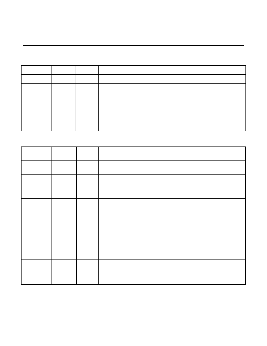
PIN DESCRIPTION
POWER
NAME
PIN
TYPE
DESCRIPTION
GND
1
I
System Ground
VDD
16
I
Power supply input, 5 V ±10%. Bypass with 0.1 and 22 µF capacitors to
GND.
VREF
31
O
An internally generated reference voltage. Bypass with 0.1 µF capacitor
to ground.
ISET
28
I
Chip current reference. Sets bias current for op-amps. The chip current is
set by connecting this pin to VDD through a 2 M
resistor. ISET should
be bypassed to GND with a 0.1 µF capacitor.
PARALLEL CONTROL INTERFACE
ALE
13
I
Address latch enable. The falling edge of ALE latches the address on
AD0-AD2 and the chip select on
CS.
AD0-AD7
5-12
I/O
Tristate
Address/data bus. These bi-directional tri-state multiplexed lines carry
information to and from the internal registers.
CS
23
I
Chip select. A low on this pin during the falling edge of ALE allows a read
cycle or a write cycle to occur. AD0-AD7 will not be driven and no
registers will be written if
CS (latched) is not active. The state of CS is
latched on the falling edge of ALE.
CLK
2
O
Output clock. This pin is selectable under processor control to be either
the crystal frequency (for use as a processor clock) or 16 times the data
rate for use as a baud rate clock in DPSK modes only. The pin defaults
to the crystal frequency on reset.
INT
20
O
Interrupt. This open drain output signal is used to inform the processor
that a detect flag has occurred. The processor must then read the detect
register to determine which detect triggered the interrupt.
INT will stay low
until the processor reads the detect register or does a full reset.
RD
15
I
Read. A low requests a read of the 73K222BL internal registers. Data
cannot be output unless both
RD and the latched CS are active or low.
RESET
30
I/with
Pulldown
Reset. An active high signal on this pin will put the chip into an inactive
state. All control register bits (CR0, CR1, Tone) will be reset. The output
of the CLK pin will be set to the crystal frequency. An internal pull-down
resistor permits power-on-reset using a capacitor to VDD.