73K224L
V.22bis/V.22/V.21/ Bell 212A/Bell 103
Single-Chip Modem
April 2000
DESCRIPTION
The 73K224L is a highly integrated single-chip
modem IC which provides the functions needed to
construct a V.22bis compatible modem, capable of
2400 bit/s full-duplex operation over dial-up lines. The
73K224L offers excellent performance and a high
level of functional integration in a single 28-pin DIP
and 44-pin TQFP package. This device supports
V.22bis, V.22, V.21, Bell 212A and Bell 103 modes of
operation, allowing both synchronous and
asynchronous communication. The 73K224L is
designed to appear to the systems designer as a
microprocessor peripheral, and will easily interface
with popular single-chip microprocessors (80C51
typical) for control of modem functions through its 8-
bit multiplexed address/data bus or via an optional
serial control bus. An ALE control line simplifies
address
demultiplexing. Data communications
normally occur through a separate serial port. The
73K224L is pin and software compatible with the
73K212L and 73K222L single-chip modem ICs,
allowing system upgrades with a single component
change.
The 73K224L operates from a single +5V supply for
low power consumption.
The 73K224L is ideal for use in either free-standing or
integral system modem products where full-duplex
(continued)
FEATURES
∑
One-chip multi-mode V.22bis/V.22/V.21 and Bell
212A/103 compatible modem data pump
∑
FSK (300 bit/s), DPSK (600, 1200 bit/s), or QAM
(2400 bit/s) encoding
∑
Pin and software compatible with other TDK
Semiconductor Corporation K-Series 1-chip
modems
∑
Interfaces directly with standard microcontrollers
(80C51 typical)
∑
Parallel microcontroller bus for modem control and
status monitoring functions
∑
Selectable
asynch/synch with internal
buffer/debuffer and scrambler/descrambler
functions
∑
All synchronous and asynchronous operating
modes (internal, external, slave)
∑
Adaptive equalization for optimum performance
over all lines
∑
Programmable transmit attenuation (16 dB, 1 dB
steps), selectable receive boost (+18 dB)
∑
Call progress, carrier, answer tone, unscrambled
mark, S1, and signal quality monitors
∑
DTMF, answer and guard tone generators
∑
Test modes available: ALB, DL, RDL, Mark, Space,
Alternating bit, S1 pattern
∑
CMOS technology for low power consumption
(typically 100 mW @ 5V) with power-down mode
(15 mW @ 5V)
∑
TTL and CMOS compatible inputs and outputs
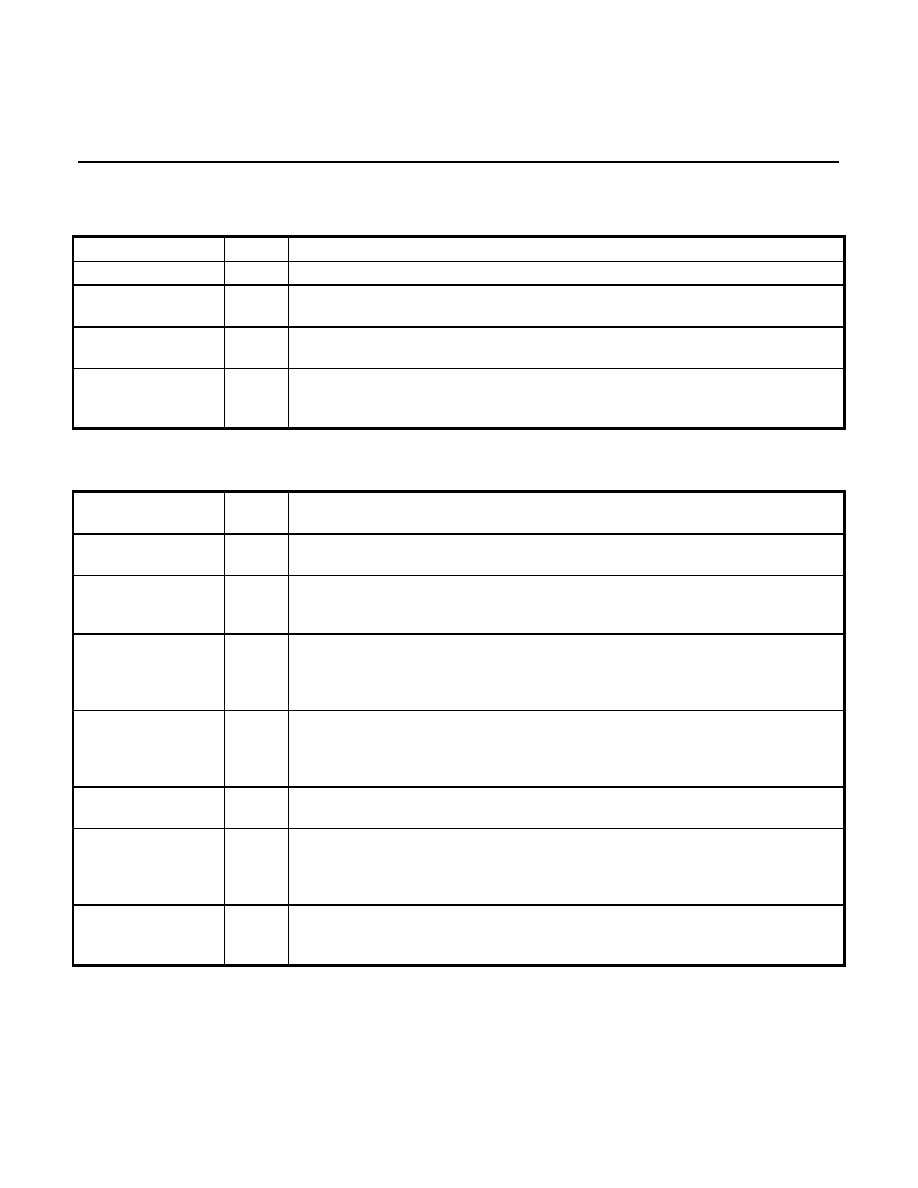
BLOCK DIAGRAM

73K224L
V.22bis/V.22/V.21/Bell 212A/Bell 103
Single-Chip Modem
2
DESCRIPTION
(continued)
2400 bit/s data communications over the 2-wire
switched telephone network is desired. Its high
functionality, low power consumption, and efficient
packaging simplify design requirements and increase
system reliability.
The 73K224L is designed to be a complete V.22bis
compatible modem on a chip. The complete modem
requires only the addition of the phone line interface, a
microcontroller for modem control and status
monitoring, and RS-232 level converters for a typical
system. Many functions were included to simplify
implementation of typical modem designs. In addition
to the basic 2400 bit/s QAM, 600/1200 bit/s DPSK and
300 bit/s FSK modulator/demodulator sections, the
device also includes SYNCH/ASYNCH converters,
scrambler/descrambler, call progress tone detect,
DTMF tone generator capabilities and handshake
pattern detectors. V.22bis, V.22, V.21 and Bell
212A/103 modes are supported (synchronous and
asynchronous) and test modes are provided for
diagnostics. Most functions are selectable as options
and logical defaults are provided.
OPERATION
QAM MODULATOR/DEMODULATOR
The 73K224L encodes incoming data into quad-bits
represented by 16 possible signal points with specific
phase and amplitude levels. The baseband signal is
then filtered to reduce intersymbol interference on the
bandlimited telephone network. The modulator
transmits this encoded data using either a 1200 Hz
(originate mode) or 2400 Hz (answer mode) carrier.
The demodulator, although more complex, essentially
reverses this procedure while also recovering the data
clock from the incoming signal. Adaptive equalization
corrects for varying line conditions by automatically
changing filter parameters to compensate for line
characteristics.
DPSK MODULATOR/DEMODULATOR
The 73K224L modulates a serial bit stream into di-bit
pairs that are represented by four possible phase
shifts as prescribed by the Bell 212A/V.22 standards.
The base-band signal is then filtered to reduce
intersymbol interference on the bandlimited 2-wire
PSTN line. Transmission occurs on either a 1200 Hz
(originate mode) or 2400 Hz carrier (answer mode).
Demodulation is the reverse of the modulation
process, with the incoming analog signal eventually
decoded into di-bits and converted back to a serial
bit stream. The demodulator also recovers the
clock which was encoded into the analog signal
during modulation. Demodulation occurs using
either a 1200 Hz carrier (answer mode or ALB
originate mode) or a 2400 Hz carrier (originate
mode or ALB answer mode). Adaptive
equalization is also used in DPSK modes for
optimum operation with varying line conditions.
FSK MODULATOR/DEMODULATOR
The FSK modulator produces a frequency
modulated analog output signal using two discrete
frequencies to represent the binary data. The Bell
103 standard frequencies of 1270 and 1070 Hz
(originate mark and space) and 2225 and 2025 Hz
(answer mark and space) are used when this
mode is selected. V.21 mode uses 980 and 1180
Hz (originate, mark and space) or 1650 and 1850
Hz (answer, mark and space). Demodulation
involves detecting the received frequencies and
decoding them into the appropriate binary value.
The rate converter and scrambler/descrambler are
automatically bypassed in the FSK modes.
PASSBAND FILTERS AND EQUALIZERS
High and low band filters are included to shape the
amplitude and phase response of the transmit and
receive signals and provide compromise delay
equalization and rejection of out-of-band signals.
Amplitude and phase equalization are necessary
to compensate for distortion of the transmission
line and to reduce intersymbol interference in the
bandlimited receive signal. The transmit signal
filtering corresponds to a 75% square root of
raised Cosine frequency response characteristic.
ASYNCHRONOUS MODE
The Asynchronous mode is used for
communication with asynchronous terminals which
may communicate at 600,1200, or 2400 bit/s +1%,
-2.5% even though the modem's output is limited
to the nominal bit rate ±.01% in DPSK and QAM
modes. When transmitting in this mode the serial
data on the TXD input is passed through a rate
converter which inserts or deletes stop bits in the
serial bit stream in order to output a signal that is
the nominal bit rate ±.01%. This signal is then
routed to a data scrambler and into the analog
modulator where quad-bit/di-bit encoding results in
the output signal. Both the rate converter and
scrambler can be bypassed for handshaking, and

73K224L
V.22bis/V.22/V.21/Bell 212A/Bell 103
Single-Chip Modem
3
synchronous operation as selected. Received data is
processed in a similar fashion except that the rate
converter now acts to reinsert any deleted stop bits
and output data to the terminal at no greater than the
bit rate plus 1%. An incoming break signal (low
through two characters) will be passed through without
incorrectly inserting a stop bit.
The SYNC/ASYNC converter also has an extended
Overspeed mode which allows selection of an output
overspeed range of either +1% or +2.3%. In the
extended Overspeed mode, stop bits are output at 7/8
the normal width.
Both the SYNC/ASYNC rate converter and the data
descrambler are automatically bypassed in the FSK
modes.
SYNCHRONOUS MODE
Synchronous operation is possible only in the QAM or
DPSK modes. Operation is similar to that of the
Asynchronous mode except that data must be
synchronized to a provided clock and no variation in
data transfer rate is allowable. Serial input data
appearing at TXD must be valid on the rising edge of
TXCLK.
TXCLK is an internally derived 1200 or 2400 Hz signal
in Internal mode and is connected internally to the
RXCLK pin in Slave mode. Receive data at the RXD
pin is clocked out on the falling edge of RXCLK. The
asynch/synch converter is bypassed when
Synchronous mode is selected and data is transmitted
at the same rate as it is input.
PARALLEL BUS INTERFACE
Eight 8-bit registers are provided for control, option
select, and status monitoring. These registers are
addressed with the AD0, AD1, and AD2
multiplexed address lines (latched by ALE) and
appear to a control microprocessor as seven
consecutive memory locations. Six control
registers are read/write memory. The detect and
ID registers are read only and cannot be modified
except by modem response to monitored
parameters.
SERIAL CONTROL MODE
The serial Command mode allows access to the
73K224 control and status registers via a serial
control port. In this mode the AD0, AD1, and AD2
lines provide register addresses for data passed
through AD7 (DATA) pin under control of the
RD
and
WR
lines. A read operation is initiated when
the
RD
line is taken low. The next eight cycles of
EXCLK will then transfer out eight bits of the
selected address location LSB first. A write takes
place by shifting in eight bits of data LSB first for
eight consecutive cycles of EXCLK.
WR
is then
pulsed low and data transfer into the selected
register occurs on the rising edge of
WR
.
DTMF GENERATOR
The DTMF generator controls the sending of the
sixteen standard DTMF tone pairs. The tone pair
sent is determined by selecting TRANSMIT DTMF
(bit D4) and the 4 DTMF bits (D0-D3) of the TONE
register. Transmission of DTMF tones from TXA is
gated by the TRANSMIT ENABLE bit of CR0 (bit
D1) as with all other analog signals.
73K224L
V.22bis/V.22/V.21/Bell 212A/Bell 103
Single-Chip Modem
4
PIN DESCRIPTION
POWER
NAME
TYPE
DESCRIPTION
GND
I
System Ground.
VDD
I
Power supply input, 5V -5% +10%. Bypass with 0.22 µF and 22 µF capacitors to
GND.
VREF
O
An internally generated reference voltage. Bypass with 0.22 µF capacitor to
GND.
ISET
I
Chip current reference. Sets bias current for op-amps. The chip current is set by
connecting this pin to VDD through a 2 M
resistor. Iset should be bypassed to
GND with a 0.22 µF capacitor.
PARALLEL MICROPROCESSOR INTERFACE
ALE
I
Address latch enable. The falling edge of ALE latches the address on AD0-AD2
and the chip select on
CS
.
AD0- AD7
I/O
/Tristate
Address/data bus. These bidirectional tri-state multiplexed lines carry infor-
mation to and from the internal registers.
CS
I
Chip select. A low on this pin allows a read cycle or a write cycle to occur. AD0-
AD7 will not be driven and no registers will be written if
CS
(latched) is not active.
CS
is latched on the falling edge of ALE.
CLK
O
Output clock. This pin is selectable under processor control to be either the
crystal frequency (for use as a processor clock) or 16 x the data rate for use as a
baud rate clock in QAM/DPSK modes only. The pin defaults to the crystal
frequency on reset.
INT
O
Interrupt. This open drain /weak pull-up, output signal is used to inform the
processor that a detect flag has occurred. The processor must then read the
detect register to determine which detect triggered the interrupt.
INT
will stay
active until the processor reads the detect register or does a full reset.
RD
I
Read. A low requests a read of the 73K224L internal registers. Data cannot be
output unless both
RD
and the latched
CS
are active or low.
RESET
I
Reset. An active high signal on this pin will put the chip into an inactive state. All
control register bits (CR0, CR1, CR2, CR3, Tone) will be reset. The output of the
CLK pin will be set to the crystal frequency. An internal pull down resistor permits
power on reset using a capacitor to VDD.
WR
I
Write. A low on this informs the 73K224L that data is available on AD0-AD7 for
writing into an internal register. Data is latched on the rising edge of
WR
. No data
is written unless both
WR
and the latched
CS
are active (low).
NOTE: The serial control mode is provided by tying ALE high and
CS
low. In this configuration AD7 becomes
DATA and AD0, AD1 and AD2 become the address only.
73K224L
V.22bis/V.22/V.21/Bell 212A/Bell 103
Single-Chip Modem
5
DTE USER INTERFACE
NAME
TYPE
DESCRIPTION
EXCLK
I
External Clock. This signal is used in synchronous transmission when the
external timing option has been selected. In the external timing mode the rising
edge of EXCLK is used to strobe synchronous transmit data available on the
TXD pin. Also used for serial control interface.
RXCLK
O/
Tristate
Receive Clock. Tri stateable. The falling edge of this clock output is coincident
with the transitions in the serial received data output. The rising edge of RXCLK
can be used to latch QAM or DPSK valid output data. RXCLK will be active as
long as a carrier is present.
RXD
O/
Weak
Pull-up
Received Digital Data Output. Serial receive data is available on this pin. The
data is always valid on the rising edge of RXCLK when in synchronous mode.
RXD will output constant marks if no carrier is detected.
TXCLK
O/
Tristate
Transmit Clock. Tri stateable. This signal is used in synchronous transmission to
latch serial input data on the TXD pin. Data must be provided so that valid data is
available on the rising edge of the TXCLK. The transmit clock is derived from
different sources depending upon the synchronization mode selection. In Internal
Mode the clock is generated internally. In External Mode TXCLK is phase locked
to the EXCLK pin. In Slave Mode TXCLK is phase locked to the RXCLK pin.
TXCLK is always active.
TXD
I
Transmit Digital Data Input. Serial data for transmission is input on this pin. In
synchronous modes, the data must be valid on the rising edge of the TXCLK
clock. In asynchronous modes (2400/1200/600 bit/s or 300 baud) no clocking is
necessary. DPSK data must be +1%, -2.5% or +2.3%, -2.5 % in extended
overspeed mode.
ANALOG INTERFACE AND OSCILLATOR
RXA
I
Received modulated analog signal input from the phone line.
TXA
O
Transmit analog output to the phone line.
XTL1
I
XTL2
I/O
These pins are for the internal crystal oscillator requiring a 11.0592 MHz parallel
mode crystal. Two capacitors from these pins to ground are also required for
proper crystal operation. Consult crystal manufacturer for proper values. XTL2
can also be driven from an external clock.