73M2901CL
V.22bis Single Chip Modem
May 2002
DESCRIPTION
The 73M2901CL is a single-chip modem that
combines all the controller (DTE) and data pump
functions necessary to implement an intelligent
V.22bis data modem.
It is adequately suited for embedded applications
where a data return channel is needed through the
telephone network such as Set top Box, Point of
Sale Terminal, Automatic Teller machine, Hand Held
Communication Device and Smart Card Reader.
This device is based on TDK Semiconductor's
implementation of the industry standard 8032
microcontroller core with a proprietary Multiply/
ACcumulate (MAC) coprocessor; Sigma-Delta A/D
and D/A converters (CODEC); and an analog DAA
drivers. The ROM and RAM necessary to operate
the modem are contained on the device.
Additionally, the 73M2901CL provides an on-chip
oscillator and hybrid.
FEATURES
∑
True one chip solution for embedded systems
∑
Low power
As low as 9.5mA operating with standby and
power down mode available
∑
Power supply operation from 3.6V to 2.7V
∑
Data speed:
V.22bis ≠ 2400bps
V.22/Bell212 ≠ 1200bps
V.21/Bell103 ≠ 300bps
V.23 ≠ 1200/75bps (with PAVI turnaround)
Bell202 ≠ 1200bps
Bell202/V23 4-wire operations
∑
International Call Progress support
FCC68, CTR21, JATE, etc.
∑
Worldwide Caller ID capability
Type I and II support
EIA 716 compliant
∑
DTMF generation and detection
∑
On chip hybrid driver
∑
Blacklisting capability
∑
Line-In-Use and Parallel Pick-Up (911) detection
capability
∑
Manufacturing Self Test capability
∑
Packaging:
32 pin PLCC / 32 pin TQFP / 44 pin LQFP
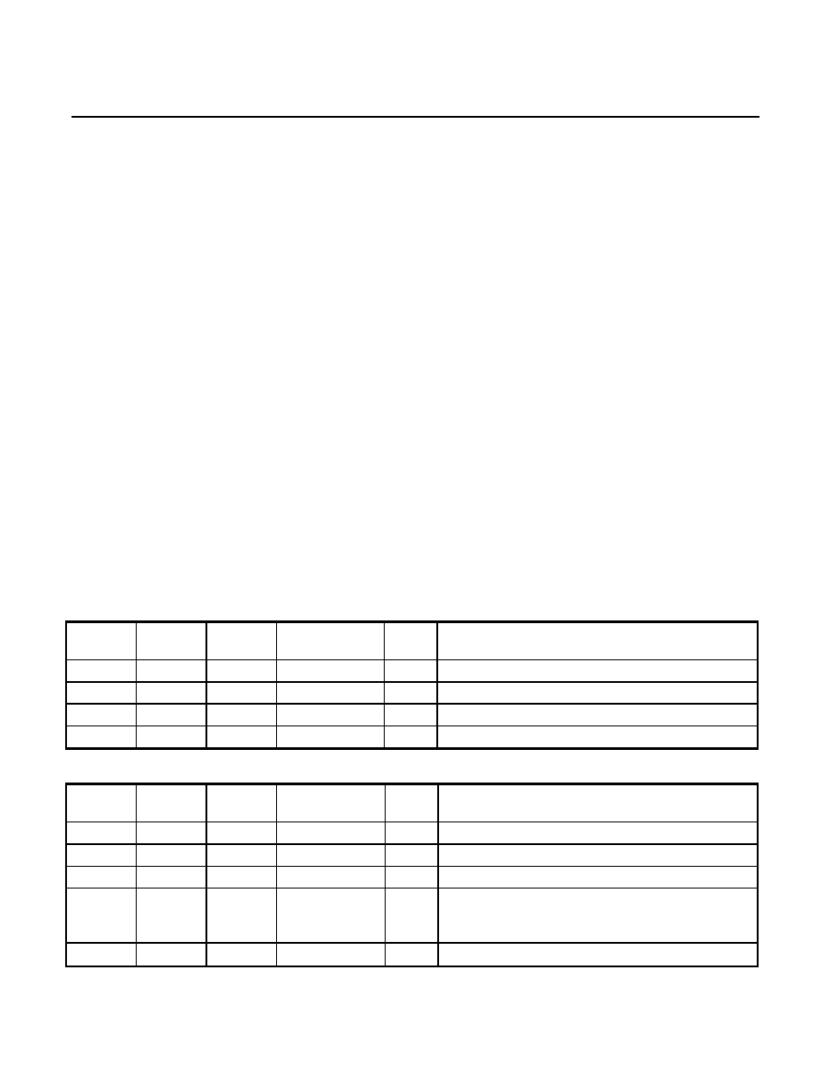
BLOCK DIAGRAM
TDK SEMICONDUCTOR CORP.
Æ

73M2901CL
V.22bis Single Chip Modem
2
HARDWARE DESCRIPTION
The 73M2901CL is designed to operate from a +3.6
to +2.7 volt supply with low power consumption
(~30mW @ 3.0 volts). The modem supports
automatic standby idle mode. The modem will also
accept a request to power down from the DTE via
hardware control. No additional major components
are required to complete the modem core logic. The
modem provides direct firmware LED support via
port pins.
HARDWARE FEATURES
∑
Fully self-contained. "AT" Command interpreter
and data pump
∑
User pins available
∑
Synchronous serial data I/O available
∑
Asynchronous serial port
∑
On-chip hybrid and line driver.
∑
Autobaud capability from 300bps to 9600bps
POWER SUPPLY
Power is supplied to the 73M2901CL via the VPD
and VPA pins. The 73M2901CL is designed for a
single +3.6 to +2.7 volt supply and for low power
consumption (~30mW @ 3.0 volts). Ground is
supplied to the 73M2901CL via VND and VNA pins.
The 73M2901CL has been designed with separated
analog and digital supplies to insure the best
performance of the part by using different filtered
power supplies. It is recommended that separate
locally bypassed traces be used to apply power to
the analog supply VPA and the digital supply VPD.
LOW POWER MODE
The TDK 73M2901CL supports a low power standby
mode. If the low power standby option is enabled the
73M2901CL will go into a power saving mode when
idle. The oscillator will be running, clocks will be
supplied to the UART, timers and interrupt blocks;
but no clocks will be supplied to the CPU. Instruction
processing and activity on the internal busses is
halted. Normal operation is resumed when an
interruption such as assertion of
'75
or
5,1*
, a
character is sent to the 73M2901CL TXD input, or a
reset occurs.
ANALOG LINE / HYBRID INTERFACE
The 73M2901CL provides a differential analog
output (TXAP and TXAN) and a single-ended analog
input (RXA) with internal A/D and D/A converters. A
driver is provided for an internal hybrid function.
The internal hybrid driver is capable of driving an
external load matching impedance and a line-
coupling transformer. The internal hybrid/line driver
senses the load and adapts itself to its requirements.
The 73M2901CL provides firmware control for a
hook relay driver (
5(/$<
) as well as interrupt
support for a ring detect opto-coupler (
5,1*
).
INTERRUPT PINS
The external interrupt sources,
'75
and
5,1*
,
come from dedicated input pins of the same name.
DTR informs the 73M2901CL that the host has
requested the 73M2901CL perform a specific
function. The function of
'75
can be changed by
"AT" commands (described in full in the TDK
73M2901CL User's Guide).
RING is used to inform the 73M2901CL that the
external DAA circuitry has detected a ring signal.
In addition, sending any character on the TXD line
also generates an internal interrupt.
CRYSTAL OSCILLATOR
The TDK 73M2901CL single chip modem can use
an external 11.0592 MHz reference clock or can
generate a clock using only a crystal and two
capacitors. If an external clock is used, it should be
applied to OSCIN.
73M2901CL
V.22bis Single Chip Modem
3
SPECIFYING A CRYSTAL
The manufacturer of a crystal resonator verifies its
frequency of oscillation in a test set-up, but to
ensure that the same frequency is obtained in the
application, the circuit conditions must be the same.
The TDK 73M2901CL modem requires a parallel
mode (anti-resonant) crystal, the important
specifications of which are as follows:
Mode: Parallel
(anti-resonant)
Frequency: 11.0592
MHz
Frequency tolerance:
±50 ppm at initial temperature.
Temperature drift:
An additional ±50 ppm over full range.
Load capacitance:
18pF or 20pF
ESR: 75
max.
Drive level:
Less than 1mW.
The peak voltage level of the oscillator should be
checked to assure it will not violate the maximum
voltage levels allowed on the oscillator pins. A
resistor in series with the crystal can be used, if
necessary, to reduce the oscillator's peak voltage
levels.
Crystals with low ESRs may oscillate at higher than
specified voltage levels.
RESET
A reset is accomplished by holding the RESET pin
high. To ensure a proper power-on reset, the reset
pin must be held high for a minimum of 3
µ
s. At
power on, the voltage at VPD, VPA, and RESET
must come up at the same time for a proper reset.
The signals
'&'
,
&76
and
'65
will be held inactive
for 25ms, acknowledging the reset operation, within
a 250ms time window after the reset-triggering
event. The 73M2901CL is ready for operation after
that 250ms window and/or after the signals
'&'
,
&76
and
'65
become active.
ASYNCHRONOUS AND SYNCHRONOUS SERIAL
DATA INTERFACE
The serial data interface consists of the TXD and
RXD data paths (LSB shifted in and out first,
respectively); and the TXCLK and RXCLK serial
clock outputs associated with the data pins;
&76
/
576
flow control;
'&'
,
'65
and
'75
. In
synchronous mode, the data is passed at the bit rate
(tolerance is +1%, -2.5%).
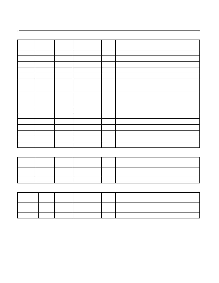
PIN DESCRIPTIONS
POWER PIN DESCRIPTION
PIN
NAME
32 pin
PLCC
32 pin
TQFP
44 pin LQFP
TYPE
DESCRIPTION
VPA
15
10
16
I
Positive analog voltage (Analog supply)
VNA
21
16
22
I
Negative analog voltage (Analog ground)
VPD
6, 25, 29
2, 20, 25
2, 12, 27, 33
I
Positive digital voltage (Digital supply)
VND
5, 22, 26
1, 17, 22
11, 24, 44, 28
I
Negative digital voltage (Digital ground)
ANALOG INTERFACE PIN DESCRIPTION
PIN
NAME
32 pin
PLCC
32 pin
TQFP
44 pin LQFP
TYPE
DESCRIPTION
RXA 20
15 21 I
Receive
Analog
input
TXAN
16
11
17
O
Transmit Analog - output
TXAP
17
12
18
O
Transmit Analog + output
VBG 19
14 20 O
Analog Band Gap voltage reference (0.1
µ
F to
VNA). This pin must not be connected to external
circuitry other than the decoupling capacitor.
VREF 18 13
19
O
Analog reference voltage (0.1
µ
F to VNA)
73M2901CL
V.22bis Single Chip Modem
4
DIGITAL INTERFACE PIN DESCRIPTION
PIN
NAME
32 pin
PLCC
32 pin
TQFP
44 pin LQFP
TYPE
DESCRIPTION
RESET 13
9
9
I
Reset
RXCLK
31
27
36
O
Receive data synchronous clock
TXCLK
28
24
31
O
Transmit data synchronous clock
TXD
27
23
30
I
Serial data input from DTE
RXD
30
26
35
O
Serial output to DTE
USR10 12 8
8
I/O
Programmable I/O port. This pin optionally be
used to control an external switch for external Line
In Use circuitry.
USR11 11 7
7
I/O
Programmable I/O port. This pin can optionally be
used to control an external switch for caller ID
operation.
576
10 6
6
I
Request
to
send
&76
9 5
5 O
Clear
to
send
'65
8 4
4 O
Data
set
ready
'&'
7 3
3 O
Data
carrier
detect
5,
4 32
43 O
Ring
indicator
5(/$<
3 31
40 O
Relay
driver
output
USR20
1
29
38
I/O
Programmable I/O port
EXTERNAL INTERRUPTS PIN DESCRIPTION
PIN
NAME
32 pin
PLCC
32 pin
TQFP
44 pin LQFP
TYPE
DESCRIPTION
5,1*
2 30
39 I
External interrupt ≠ Line interface ring detection
circuitry input
'75
32 28
37
I
External
interrupt
≠ DTE DTR signal input
OSCILLATOR PIN DESCRIPTION
PIN
NAME
32 pin
PLCC
32 pin
TQFP
44 pin LQFP
TYPE
DESCRIPTION
OSCIN 24 19
26
I
Crystal input for internal oscillator, also input for
external source
OSCOUT 23 18
25
O
Crystal
oscillator
output
73M2901CL
V.22bis Single Chip Modem
5
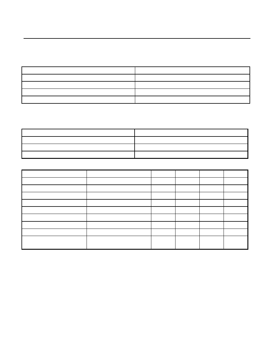
ELECTRICAL SPECIFICATIONS
ABSOLUTE MAXIMUM RATINGS
PARAMETER RATING
Supply Voltage
-0.5V to +4.0V
Pin Input Voltage (except OSCIN)
-0.5V to + 6.0V
Pin Input Voltage (OSCIN)
-0.5V to VPD + 0.5V
Storage Temperature
-55∫C to 150∫C
NOTE: This is a stress rating only and functional operation of the device at these or any other conditions above those indicated in the operation sections
of this specification is not implied. Exposure to absolute maximum conditions for extended periods of time may affect reliability.
RECOMMENDED OPERATING CONDITIONS
PARAMETER RATING
Supply Voltage
2.7V ≠ 3.6V
Oscillator Frequency
11.0592MHz +/- 50ppm
Operating Temperature
-40∫C to 85∫C
RECEIVER
PARAMETER
CONDITIONS
MIN NOM MAX UNIT
Carrier detect On
Tip and Ring
-43
dBm0
*
Carrier detect Off
Tip and Ring
-48
dBm0
*
Carrier Detect Hysteresis
Tip and Ring
2
dB
Receive Level
Tip and Ring
-43
-9
dBm0
*
Idle channel noise
0.2KHz ≠ 4.0KHz
-70
-65
dB
Input impedance
RXA
150
k
Receive Gain Boost
SFR 96.2h = 1
18.8
19.3
19.8
dB
Max Input Level at RxA
Vref=1.25V
0.587
0.622
0.658
Vpk
Total Harmonic Distortion
(THD)
1KHz 450mVpk on RXA
THD=2
nd
and 3
rd
harmonic
-70
-50
dB
*
dBm0 refers to the TDK recommended line interface (8dB loss from transmit pins to the line and 5dB loss from the line to the receiver pin). Results
may vary depending on the selected DAA components. 0dBm=0.775mV
rms
; dBm=10log(V
rms
2
/(1mW)(600
))