 | –≠–ª–µ–∫—Ç—Ä–æ–Ω–Ω—ã–π –∫–æ–º–ø–æ–Ω–µ–Ω—Ç: 73M2921 | –°–∫–∞—á–∞—Ç—å:  PDF PDF  ZIP ZIP |

Rev M
Advanced Information
73M2921
Advanced Single
Chip Modem
February 1999
DESCRIPTION
The 73M2921 is a CMOS integrated circuit which
provides all the modem "Data Pump" functions
required to implement a V.22bis data modem. It
consists of a DSP (Digital Signal Processor) core
with RAM and ROM data memory, ROM instruction
memory, and register mapped input/output functions
including timers, interrupts,
ADC and DAC ports
and Serial Data I/O.
Once the 73M2921 has been initialized, all call
progress and modem handshaking is automatic.
The default conditions may be changed as required
for country specific or custom applications.
The 73M2921 provides DTMF tone generation and
detection, precise call progress detect and ADSI
functions such as CAS tone detection.
Other features include a parallel interface control
port between the host processor and the 73M2921.
A synchronous serial data channel provides
synchronizing clocks RXCLK and TXCLK from the
modem pump to the controller.
The 73M2921 contains an oscillator and power
control features.
The host controller function can be implemented with
a 73M2910 communications micro controller or
another commercial microcontroller (such as the
68302). The 73M2921 has been optimized to work
with the 73M2910 synchronous serial port.
FEATURES
∑
Automatic handshaking for all data modes
∑
Data Speeds:
V.22bis - 2400 b/s
V.22, Bell 212 - 1200 b/s
V.21, Bell 103 - 300 b/s
V.23 1200 b/s - 75 b/s
Bell 202 1200 b/s
∑
Facsimile Speeds:
V.29 - 9600, 7200 b/s
V.27ter - 4800, 2400 b/s
V.21 ch 2 - 300 b/s
∑
V.8bis applications
∑
Designed for 3.3 and 5-Volt systems.
∑
Low operating power.
∑
Speaker monitor output
∑
Provides 2 tone generators for single tone or
DTMF generation
∑
Provides DTMF tone detection
∑
Provides 4 precise and 1 imprecise call
progress filters and corresponding detect
bits with programmable thresholds and
frequencies
∑
Provides CAS tone detection for ADSI and
CLASS
Æ
feature support
∑
Supports parallel (8 bit) control, and
synchronous serial data I/O
∑
73M2921 provides a microcontroller inter-
rupt
∑
Packaging: The 73M2921 is available in a
QFP production package. A PGA package is
available for prototyping
73M2921
Advanced Single
Chip Modem
Page 2 of 41
TDK Semiconductor
February 99 Rev M
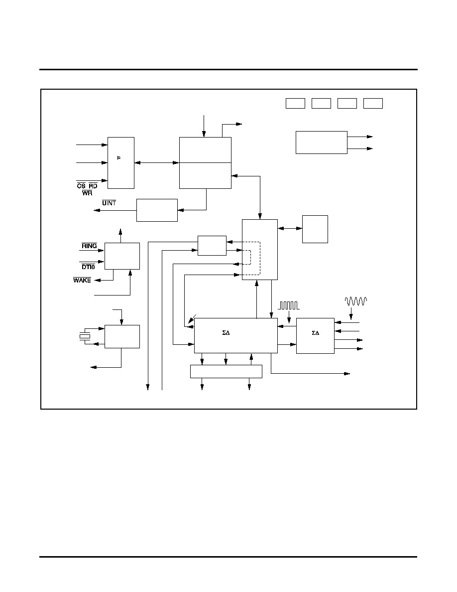
FIGURE 1 - Block Diagram
P
PORT
CR0
MAILBOX
READ THE
MAILBOX
RAM/
ROM
VOLTAGE
REFERENCE
SERIAL
DATA
POWER
UP
DSP
CLOCKS
TIMER
(MODULATOR & DECIMATOR)
(ADC &DAC)
SERIAL CLOCKS
14.4 KHz Samples
CTRL
XTALI
XTALO
CLK CTRL
MICCLK
RESET
PWR UP
INTERRUPTS
TXD
RXD
TXCLK
RXCLK
CLK CNTRL
DIGITAL
BIT STREAM
MON
INPA
INNA
OUTPA
OUTNA
ANALOG
VBG
VREF
PWR UP
UA[0-1]
UD[0-7]
,
VPD
VPA
VND
VPA
73M2921
Advanced Single
Chip Modem
February 99 Rev M
TDK Semiconductor
Page 3 of 41
PIN DESCRIPTION
POWER
NAME
PIN
TYPE
DESCRIPTION
VPD
3, 23,
51, 82
I
DIGITAL POWER: Positive Digital Power.
VND
4, 20,
52, 74
I
DIGITAL POWER: Negative Digital Power.
VPA
29, 36
I
ANALOG POWER: Positive Analog Power.
VNA
27, 37
I
ANALOG POWER: Negative Analog Power.
VREF
32
O
VREF: Analog voltage reference for biasing of off chip analog function.
Maximum output current is +/- 20
µ
A.
VBG
33
O
BANDGAP VOLTAGE: Bandgap voltage pin used as a connection point
for an external capacitor for noise reduction only.
CLOCKS AND RESETS
NAME
PIN
TYPE
DESCRIPTION
XTALI
22
I
CRYSTAL INPUT: Onboard crystal oscillator input, or the master clock
input to the 73M2921 if the crystal oscillator is not used.
XTALO
21
I
CRYSTAL OUTPUT: Onboard crystal oscillator output should be left
unconnected if the crystal oscillator on the 73M2921 is not used. Along
with XTALI and proper loading capacitors, these pins include an inverter
for use with parallel resonant mode crystals.
MICCLK
19
O
MICROCONTROLLER CLOCK: Programmable clock output for use
when the system oscillator is on the 73M2921. May be used to drive the
system controller. The output frequency is controlled by CR0 bits D11-
D9 (MCLK [2:0]).
RESET
40
I
MASTER CHIP RESET: Active High Input with hysteresis. Resets the
73M2921 and the control registers. If not used as a reset source, this
pin must be tied low.
73M2921
Advanced Single
Chip Modem
Page 4 of 41
TDK Semiconductor
February 99 Rev M
PIN DESCRIPTION
(continued)
POWER CONTROL
NAME
PIN
TYPE
DESCRIPTION
'7,�
26
I
DATA TERMINAL INTERRUPT 0: Active Low Input with hysteresis.
Power up signal. The action of this pin can be masked by the PSDIS[1]
register bit. This pin would connect to EIA-232 connection DTR in many
applications. Requires a 50K
external pull up.
5,1*
24
I
RING DETECT: Active Low Input with hysteresis. Power up signal. The
action of this pin can be masked by the PSDIS[0] register bit. This pin
would connect to the ring detect circuitry or the control microcontroller in
many applications. Requires a 50K
external pull up.
:$.(
39
O
WAKE: Active Low Output. Indicates that a power up pin (
5,1*
or
'7,�
) has been activated when the 73M2921 is in slave mode. The
latched signal remains true until a reset of the wake function by a write to
CR0 LSByte, or a chip reset. Requires a 50K
external pull up.
MICROCONTROLLER INTERFACE
NAME
PIN
TYPE
DESCRIPTION
&6
15
I
CHIP SELECT: Active Low Input. Enables data transfers on the
µ
P
parallel interface. Requires a 50K
external pull up.
5'
17
I
READ: Active Low Input. Read enable signals for the mailbox/control
register interface.
:5
16
I
WRITE: Active Low Input. Write enable signals for the mailbox/control
register interface.
UA[0:1]
13-14
I
ADDRESS: Address bits that are used by the
µ
P to communicate with
the 73M2921 mailbox and CR0.
UD [0:7]
5-12
I/O
DATA: Parallel data bus for the mailbox/CR0 interface.
8,17
18
O
INTERRUPT:
µ
C interrupt Active Low Output. Used as an interrupt to
the microcontroller indicating that the 73M2921 needs data or has a
request for the
µ
C. It is activated when the 73M2921 writes to the
mailbox and cleared when the µC reads the mailbox LSByte. Requires a
50K
external pull up.
73M2921
Advanced Single
Chip Modem
February 99 Rev M
TDK Semiconductor
Page 5 of 41
PIN DESCRIPTION
(continued)
SERIAL DATA INTERFACE
NAME
PIN
TYPE
DESCRIPTION
RXCLK
45
O
RECEIVE CLOCK: Receive clock for the serial data interface. Data is
transferred from the 73M2921 on the rising edge of the clocks.
TXCLK
42
O
TRANSMIT CLOCK: Transmit clock for the serial data interface. Data is
transferred to the 73M2921 on the rising edge of the clocks.
RXD
44
O
RECEIVE DATA: Receive Digital Data.
TXD
41
I
TRANSMIT DATA: Transmit Digital Data.
AUXILIARY FUNCTIONS
NAME
PIN
TYPE
DESCRIPTION
MON
38
O
MONITOR: Speaker driver. PCM output under software control. See
app note concerning the use of this pin.
PEXT
50
I
EXTERNAL PROGRAM ENABLE: This pin must be tied low for normal
operation.
ANALOG I/O
NAME
PIN
TYPE
DESCRIPTION
INPA,
INNA
34,
35
I
ANALOG INPUT: Differential analog input to a high resolution ADC.
OUTPA,
OUTNA
31,
30
O
ANALOG OUTPUT: Differential analog output from a high resolution
DAC.
HARDWARE REQUIREMENTS
The 73M2921 chip is designed for a single +3.3 or 5 Volt supply and for minimum power consumption
(~100mW @ 3.3V). It supports power down (idle) mode via microcontroller software control. It will also accept
a request for power down from the DTE via hardware control. The device operates from internal ROM/RAM,
but may be configured for external ROM operation and external RAM access (for custom applications) using
either the prototype or the production packages.
LINE/HYBRID INTERFACE
The 73M2921 chip provides a differential analog input and output. This interface will drive a standard Data
Access Arrangement (DAA). The system controller provides additional control such as hook, phone and
auxiliary relay, parallel pickup and in-use detect, and ring detect.
The Internal DAC provides a differential output signal with a maximum output swing of 1.2Vpp, capable of
driving a 50K
load. One output can be used alone for a single ended output (with possible performance
degradation).
The internal ADC has a differential input maximum of 1.2Vpp, and provides a biasing resistor to Vref for AC
coupling. One input can be driven while leaving the other floating for a single ended input (with possible
performance degradation). The signal passes through a passive anti-aliasing filter.