 | –≠–ª–µ–∫—Ç—Ä–æ–Ω–Ω—ã–π –∫–æ–º–ø–æ–Ω–µ–Ω—Ç: 75T2090 | –°–∫–∞—á–∞—Ç—å:  PDF PDF  ZIP ZIP |
75T2089/2090/2091
DTMF Transceivers
April 2000
DESCRIPTION
TDK Semiconductor's 75T2089/2090/2091 are
complete Dual-Tone Multifrequency (DTMF)
Transceivers that can both generate and detect all
16 DTMF tone-pairs. These ICs integrate the
performance-proven 75T202 DTMF receiver with a
DTMF generator circuit.
The DTMF receiver electrical characteristics are
identical to the standard 75T202 device
characteristics. The DTMF generator provides
performance similar to the Mostek MK5380, but with
an improved (tighter) output amplitude range
specification and with the addition of independent
latch and reset controls.
An additional feature of the 75T2090/2091 is
"imprecise" call progress detector. The detector
detects the presence of signals in the 305-640 Hz
band.
(continued)
FEATURES
∑
DTMF Generator and Receiver on one-chip
∑
Call progress detection (2090/2091 only)
∑
Early detect output (2091 only)
∑
DTMF Receiver exhibits excellent speech
immunity
∑
Analog input range from -32 to -2 dBm
(ref 600
)
∑
Three-state outputs (4-bit hexadecimal) from
DTMF Receiver
∑
AC coupled, internally biased analog input
∑
Latched DTMF Generator inputs
∑
DTMF output typ. -8 dBm (Low Band) and
-5.5 dBm (High Band)
∑
Easy interface for microprocessor dialing
∑
Uses inexpensive 3.579545 MHz crystal for
reference
∑
Low-power 5 volt CMOS
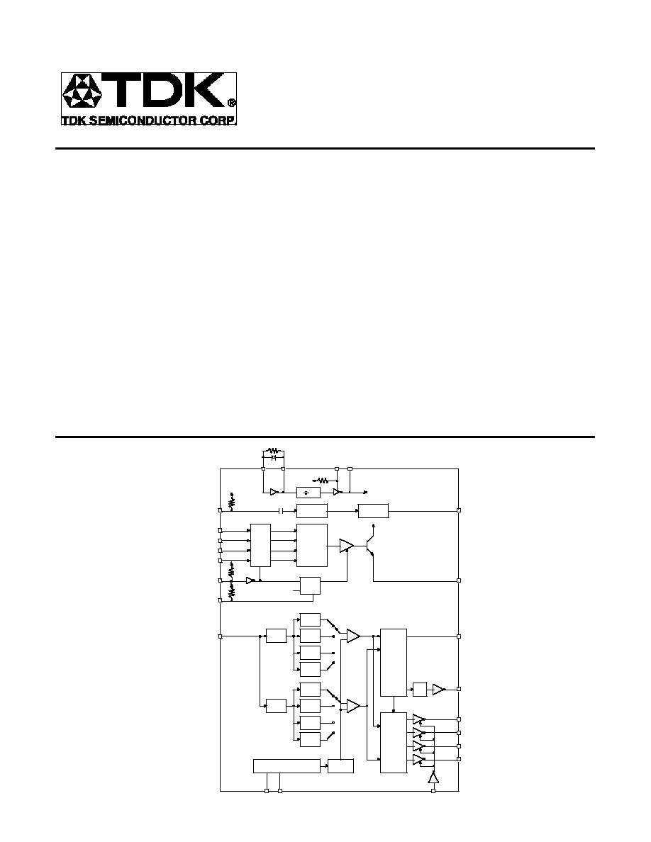
BLOCK DIAGRAM
INTERNAL
CLOCK
ATB
XEN
RS
X1
XOUT
XIN
LIN
(2090/2091 only)
D7
D6
D5
D4
LATCH
RESET
DIN
Vp
Vn
DE
D0
D1
D2
D3
DV
ED
(2091 only)
DTMF
OUT
DET
(2090/2091 only)
POWER REGULATOR
VOLTAGE
REF
BS1
BS2
697
770
852
941
1209
1336
1477
1633
BANDPASS
FILTERS
AMPLITUDE
DETECTORS
BANDPASS
FILTERS
Vp
Vp
Vp
D
Q
D
Q
D
Q
D
Q
CK
CK
D
Q
CLR
DTMF
GENERATOR
BANDSPLIT
FILTERS
8
Vp
ENERGY
DETECTOR
Vp
TIMING
CIRCUITRY
DV
STROBE
DV
F.F.
OUTPUT
DECODER
AND
REGISTER

75T2089/2090/2091
DTMF Transceivers
2
DESCRIPTION
(continued)
The 75T2091 also incorporates an early detect
function which is useful in multi-channel radio
scanning applications. The only external
components necessary for the 75T2089/2090/2091
are a 3.58 MHz "colorburst" crystal with a parallel 1
M
resistor. This provides the time base for digital
functions and switched-capacitor filters in the device.
No external filtering is required.
CIRCUIT OPERATION
RECEIVER
The DTMF Receiver in the 75T2089/2090/2091 detects
the presence of a valid tone pair (indicating a single
dialed digit) on a telephone line or other transmission
medium. The analog input is pre-processed by 60 Hz
reject and band-splitting filters, then hard-limited to
provide Automatic Gain Control. Eight bandpass filters
detect the individual tones. The digital post-processor
times the tone durations and provides the correctly
coded digital outputs. The outputs will drive standard
CMOS circuitry, and are three-state enabled to facilitate
bus-oriented architectures.
DIN
This pin accepts the analog input. It is internally
biased so that the input signal may be AC coupled.
The input may be DC coupled as long as it does not
exceed the positive supply. Proper input coupling is
illustrated in Figure 1.
The IC is designed to accept sinusoidal input
waveforms but will operate satisfactorily with any
input that has the correct fundamental frequency
with harmonics greater than -20 dB below the
fundamental.
CRYSTAL OSCILLATOR
The IC contains an onboard inverter with sufficient
gain to provide oscillation when connected to a low-
cost television "colorburst" crystal. The crystal is
placed between XIN and XOUT in parallel with a
1M
z
resistor, while XEN is tied high. Since the
switched-capacitor-filter time base is derived from
the crystal oscillator, the frequency accuracy of all
portions of the IC depends on the time base
tolerance. The DTMF Receiver frequency response
and timing is specified for a time base accuracy of at
least
=
0.005%. ATB is a clock output with the
frequency of 1/8 of crystal. Other devices may use
the same frequency reference by tying their ATB
pins to the ATB of a crystal connected device. XIN
and XEN of the auxiliary devices must then be tied
high and low respectively, XOUT is left floating.
XOUT is designed to drive a resonant circuit only
and is not intended to drive additional devices. Ten
devices may run off a single crystal-connected
transceiver as shown in Figure 2.
Vp
VIN<VP
DIN
GND
10 pF
>100 k
(On Chip)
Vp
VIN>VP
DIN
GND
10 pF
>100 k
(On Chip)
0.01 µF
8
8
FIGURE 1: Input Coupling
75T20XX
XIN
XEN
XEN
ATB
ATB
XOUT
XIN Connected to VP
VP
Up to 10 Devices
75T20XX
FIGURE 2: Crystal Connections
75T2089/2090/2091
DTMF Transceivers
3
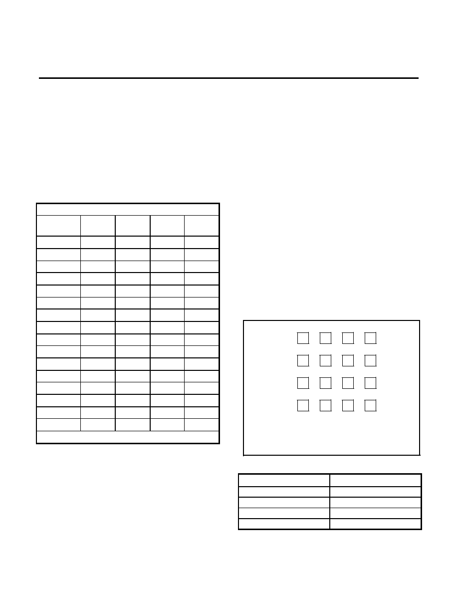
RECEIVER OUTPUTS AND THE
DE
PIN
Outputs D0, D1, D2, D3 are CMOS push-pull when
enabled (
DE
low) and open-circuited (high
impedance) when disabled (
DE
high). These digital
outputs provide the hexadecimal code
corresponding to the detected digit. Figure 3 shows
that code.
The digital outputs become valid and DV signals a
detection after a valid tone pair has been sensed.
The outputs and DV are cleared when a valid pause
has been timed.
Hexadecimal Code
Digit In
Out
D7
D3
D6
D2
D5
D1
D4
D0
1
0
0
0
1
2
0
0
1
0
3
0
0
1
1
4
0
1
0
0
5
0
1
0
1
6
0
1
1
0
7
0
1
1
1
8
1
0
0
0
9
1
0
0
1
0
1
0
1
0
*
1
0
1
1
#
1
1
0
0
A
1
1
0
1
B
1
1
1
0
C
1
1
1
1
D
0
0
0
0
FIGURE 3
ED OUTPUT (75T2091 only)
The ED output goes high as soon as the 75T2091
begins to detect a DTMF tone pair and falls when the
75T2091 begins to detect a pause. The D1, D2, D4,
and D8 outputs are guaranteed to be valid when DV
is high, but are not necessarily valid when ED is high.
GENERATOR
The DTMF generator responds to a hexadecimal
code input with a valid tone pair. Pins D4-D7 are the
data inputs for the generator. A high to low transition
on
LATCH
causes the hexadecimal code to be
latched internally and generation of the appropriate
DTMF tone pair to begin. The DTMF output is
disabled by a high on RESET and will not resume
until new data is latched in.
DIGITAL INPUTS
The D4, D5, D6, D7,
LATCH
, RESET inputs to the
DTMF generator may be interfaced to open-collector
TTL with a pull-up resistor or standard CMOS. These
inputs follow the same hexadecimal code format as the
DTMF receiver output. Figure 4 shows the code for
each digit. The dialing matrix and detection frequency
table below list the frequencies of the digits.
DETECTION FREQUENCY
Low Group f
0
High Group f
0
Row 0 = 697Hz
Column 0 = 1209Hz
Row 1 = 770Hz
Column 1 = 1336Hz
Row 2 = 852Hz
Column 2 = 1477Hz
Row 3 = 941Hz
Column 3 = 1633Hz
Col 0
Col 1
Col 2
Col 3
Row 1
Row 2
Row 3
1
4
7
*
2
5
8
0
3
6
9
#
A
B
C
D
Row 0
NOTE: Column 3 is for special applications
and is not normally used in telephone dialing.
FIGURE 4: DTMF Dialing Matrix
DE

75T2089/2090/2091
DTMF Transceivers
4
DTMF OUT
The output amplitude characteristics listed in the
specifications are given for a supply voltage of 5.0V.
However, the output level is directly proportional to
the supply, so variations in it will affect the DTMF
output. A recommended line interface for this output
is shown in Figure 5.
CALL PROGRESS DETECTION
(75T2090/2091)
The 75T2090/2091 have a Call Progress Detector
that consists of a bandpass filter and an energy
detector for turning the on/off cadences into a
microprocessor compatible signal.
DET OUTPUT (75T2090/2091)
The output is TTL compatible and will be of a
frequency corresponding to the various candences
of Call Progress signals such as: on 0.5 sec/off 0.5
sec for a busy tone, on 0.25 sec/off 0.25 sec for a
reorder tone and on 0.8-1.2 sec/off 2.7-3.3 sec for
an audible ring tone.
LIN INPUT (75T2090/2091)
This analog input accepts the call progress signal
and should be used in the same manner as the
receiver input DIN.
FIGURE 5: DTMF Output
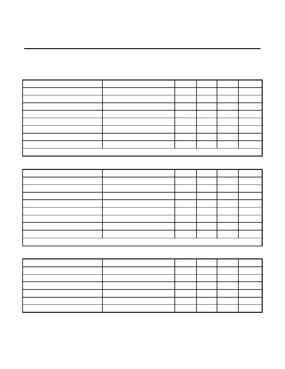
ELECTRICAL SPECIFICATIONS
ABSOLUTE MAXIMUM RATINGS
Operating above absolute maximum ratings may damage the device.
PARAMETER
RATING
DC Supply Voltage (Vp - Vn)
+7V
Voltage at any Pin (Vn = 0)
-0.3 to Vp + 0.3V
DIN Voltage
Vp + 0.5 to Vp - 10V
Current through any Protection Device
=
20mA
Operating Temperature Range
-40 to + 85
∞
C
Storage Temperature
-65 to 150
∞
C
RECOMMENDED OPERATING CONDITIONS
PARAMETER
CONDITIONS
MIN
NOM
MAX
UNIT
Supply Voltage
4.5
5.5
V
Power Supply Noise (wide band)
10
mVp-p
Ambient Temperature
-40
+85
∞
C
Crystal Frequency
-0.01
+0.01
%
(F Nominal = 3.579545MHz)
Crystal Shunt Resistor
0.8
1.2
M
DTMF OUT Load Resistance
100
DTMF
OUT
1:1
TIP
100
RING
75T2089/2090/2091
DTMF Transceivers
5
DIGITAL AND DC REQUIREMENTS
The following electrical specifications apply to the digital input and output signals over the recommended
operating range unless otherwise noted. The specifications do not apply to the following pins: LIN, DIN, XIN,
XOUT, and DTMF OUT. Positive current is defined as entering the circuit. Vn = 0 unless otherwise stated.
PARAMETER
CONDITIONS
MIN
NOM
MAX
UNIT
Supply Current*
15
30
mA
Power Dissipation
225
mW
Input Voltage High
0.7Vp
V
Input Voltage Low
0.3Vp
V
Input Current High
10
µ
A
Input Current Low
-10
µ
A
Output Voltage High
Ioh = -0.2mA
Vp-0.5
V
Output Voltage Low
IoI = +0.4mA
Vn+0.5
V
* with DTMF output disabled
DTMF RECEIVER: Electrical Characteristics
PARAMETER
CONDITIONS
MIN
NOM
MAX
UNIT
Frequency Detect Bandwidth
=
(1.5+2Hz)
=
2.3
=
3.5
%Fo
Amplitude for Detection
Each Tone
-32
-2
dBm/tone
Twist Tolerance
-10
+10
dB
60Hz Tolerance
0.8
Vrms
Dial Tone Tolerance
Precise Dial Tone
0
dB*
Speech Immunity
MITEL Tape #CM7290
2
hits
Noise Tolerance
MITEL Tape #CM7290
-12
dB*
Input Impedance
100
k
* Referenced to lowest amplitude tone
DTMF RECEIVER: Timing Characteristics
PARAMETER
CONDITIONS
MIN
NOM
MAX
UNIT
TON
Tone Time for Detect
40
ms
TON
Tone Time for No Detect
20
ms
TOFF Pause Time for Redetection
40
ms
TOFF Pause Time for Bridging
20
ms
TD1
Detect Time
25
46
ms
TR1
Release Time
35
50
ms