
78P2341JAT
E3/DS3/STS-1 LIU
with Jitter Attenuator
PRELIMINARY DATASHEET
- 1 -
AUGUST 2003
DESCRIPTION
The 78P2341JAT is a low-power, single channel
DS3/E3/STS1 transceiver IC with integrated Jitter
Attenuator (JAT). It includes clock recovery and
transmitter pulse shaping functions for applications
using 75-ohm coaxial cable at distances up to 1350
feet. These applications include DSLAMs, T1,3/E1,3
digital multiplexers, SONET Add/Drop multiplexers,
PDH equipment, DS3 to Fiber optic and microwave
modems, and ATM WAN access for routers and
switches.
The receiver recovers clock and data from a B3ZS
or HDB3 coded AMI signal. It can compensate for
over 12dB of cable and 6dB of flat loss. The
transmitter generates a signal that meets the
standard pulse shape requirements. It has an
integrated B3ZS/HDB3 ENDEC with a receive line
code violation detector, a loop-back mode, a clock
polarity selection mode, and the ability to receive a
DSX3 monitor signal.
STANDARDS
∑ Jitter Tolerance: Telcordia GR-499-CORE [DS3]
and GR-253-CORE [STS1], ITU-T G.823 [E3]
and G.824 [DS3]
∑ Loss of Signal: ITU-T G.775
∑ Jitter Transfer: ETSI TBR-24 1997 [E3];
Telcordia GR-499-CORE [DS3] and GR-253-
CORE [DS3/STS1]
FEATURES
∑ Transmit and receive interface for E3, DS3 and
STS-1 applications
∑ Designed for use with 75 ohm coaxial cable up
to 1350 ft long end-to-end or up to 900 ft long
from a DS3 cross-connect
∑ Receive DS3-high and DSX3 monitor signals
∑ Local and Remote loopback
∑ Selectable B3ZS/HDB3 ENDEC with line code
violation detector
∑ Standards-based LOS function
∑ Optional serial-port based mode selection and
channel status monitoring
∑ Receiver AGC corrects for up to 6dB of flat loss
∑ Adaptive digital clock recovery (uses line-rate
reference clock input)
∑ Receive output clock maintains nominal line-rate
frequency at all times
∑ Fully integrated Jitter Attenuator (no external
VCXO required) configurable for transmit or
receive path
∑ Transmit line fault monitor
∑ Requires no external current-setting resistor or
loop filter components
∑ Single 3.3V supply operation
∑ Available in 28-pin PLCC or 48-pin TQFP
BLOCK DIAGRAM
LOUTN
LOUTP
TPOS
TNEG
TCLK
RCLK
RPOS
RNEG
DS3
TXEN
LLBK
RLBK
PDTX
ENDEC
TXNW
Control
Registers
SCK
SDIO
E3
LBO
Master
Bias
Generator
CKREF
CKREF
LOS
Attenuator
Power
Distribution
B3ZS /
HDB3
Encoder
Data
Detector
B3ZS /
HDB3
Decoder
Adaptive
Equalizer
Signal
Detector
Transmit
Monitor
Pulse
Shaper
Controls
Jitter
Attenuator
Flags
TCLKP
RCLKP
Clock
Recovery
PDRX
LINN
LINP
MON
AGC

78P2341JAT
E3/DS3/STS-1 LIU
with Jitter Attenuator
- 2 -
FUNCTIONAL DESCRIPTION
The 78P2341JAT contains all the necessary
transmit and receive circuitry for connection
between E3, DS3, or STS-1 interfaces and
Framer/Mapper ICs.
OPERATING RATE
The Master Control Register (MSCR) determines
which mode the device operates in according to the
table below. The MSL0 pin is also provided for
mode selection in applications without a serial
control interface. Upon power-up or reset, the state
of the MSL0 pin is sensed and mapped into the DS3
and E3 register bits representing the appropriate
mode of operation. After power-up/reset, the state of
the MSL0 pin is ignored.
Standard
MSL0 pin
DS3 bit
E3 bit
E3
L 0 1
DS3 H
1
0
STS-1 Z 0 0
STS-1 Z 1 1
RECEIVER OPERATION
The receiver inputs LINP and LINN are either
transformer-coupled or capacitor-coupled to the line
signal. In applications where the highest
performance and isolation are required, a 1:1
transformer is used in the receive path. In
applications where isolation is provided elsewhere in
the circuit, capacitor coupling can be used. The
receiver inputs should be line terminated externally
with a termination resistor.
The AMI signal first enters an AGC, which has a
selectable gain range setting. In normal operation,
the AGC can compensate for signals with up to 6dB
of flat loss. When Receiver Monitor Mode is
enabled, the AGC can compensate for a DSX3
monitor signal with 16 to 20 dB of flat loss. The
signal then enters a high performance adaptive
equalizer. The equalizer is designed to overcome
inter-symbol interference caused by long cable
lengths. Because the equalizer is adaptive, the
circuit will work with all square-shaped signals such
as DS3-high or 34.368 Mbit/s E3. The variable gain
differential amplifier automatically controls the gain
to maintain a constant voltage level output
regardless of the input voltage level.
The jitter tolerance of 78P2341JAT meets the
requirements of ITU-T G.823 for E3 rates; the
requirements of ITU-T G.824, GR-499 (Cat I and II)
for DS3 rates; and the requirements of GR-253 for
STS1 rates.
When the Jitter Attenuator is disabled, the jitter
transfer function meets the requirements of GR-499
for Category II DS3 interfaces.
When the Jitter Attenuator is enabled, the
78P2341JAT meets the requirements of GR-499
and GR-253 for all categories of DS3/STS1
equipment and the ETSI TBR-24 requirements for
E3 rates. To check conformance with other
standards, please refer to the JITTER
ATTENUATOR TRANSFER FUNCTION section for
more detailed info.
REFERENCE CLOCK
The clock recovery system employs a digital PLL,
which uses a line-rate reference clock frequency.
This reference frequency can be input to the CKREF
pin or it can utilize the transmitter clock input TCLK
when CKREF is left floating or pulled high.
RECEIVER MONITOR MODE
When the MON pin is high, 20dB of flat gain is
applied to the incoming signal before it is fed to the
receive equalizer. Alternately, the MON bit in the
Mode Control Register can be used if the Register
Control bit, REGEN, is enabled.
SIGNAL DETECT
When the received signal is below a minimum
threshold, the LOS signal (bit) in the Status Monitor
register is asserted. A time delay is provided before
this output is active so that transient interruptions do
not cause false indications. By default, the LOS
signal is also used to trigger an interrupt on the
LOS
pin. Note that the error events that control the
assertion of the
LOS pin can be configured in the
Interrupt Control Register (INTC).
Note: In DS3 or STS-1 mode, when LBO is not
enabled, the transmitters have to be properly
terminated to ensure reliable LOS detection. If a
transmitter is not terminated, the resultant 2x signal
is large enough to couple to the neighboring
receivers through the ESD diodes, causing false
Signal Detect indication.

78P2341JAT
E3/DS3/STS-1 LIU
with Jitter Attenuator
- 3 -
LOOPBACK MODES
The
LPBK pin is used to activate common loopback
modes as shown in the table below. The LLBK and
RLBK bits in the Mode Control Register can also
control these modes when the Register Control bit,
REGEN, is enabled.
LPBK
pin
Loopback Mode
L
Local (Analog) Loopback
Same as LLBK = `1'
Z
Remote (Digital) Loopback
Same as RLBK = `1'
H
Normal Operation
Same as LLBK, RLBK = `0'
When in Local (Analog) Loopback, the transmit
output signals, LOUTP,N are internally routed to the
receiver inputs. Any incoming signals on LINP,N will
be ignored when in Local Loopback. For proper
operation in this mode, the transmitter needs to be
properly terminated with no hanging cables.
LOUTN
LOUTP
TPOS
TNEG
TCLK
RCLK
RPOS
RNEG
DS3
TXEN
LLBK
RLBK
PDTX
ENDEC
TXNW
Control
Registers
SCK
SDIO
E3
LBO
Master
Bias
Generator
CKREF
CKREF
LOS
Attenuator
Power
Distribution
B3ZS /
HDB3
Encoder
Data
Detector
B3ZS /
HDB3
Decoder
Adaptive
Equalizer
Signal
Detector
Transmit
Monitor
Pulse
Shaper
Controls
Jitter
Attenuator
Flags
TCLKP
RCLKP
Clock
Recovery
PDRX
LINN
LINP
MON
AGC
Local (Analog) Loopback
Tx JAT Off
Tx JAT On
Rx JAT On
Rx JAT Off
When in Remote (Digital) Loopback, the received
signals and clock data, RPOS/RNEG/RCLK, are
internally routed to the transmitter input signals. Any
incoming data on TPOS, TNEG, or TCLK will be
ignored when in Remote Loopback.
LOUTN
LOUTP
TPOS
TNEG
TCLK
RCLK
RPOS
RNEG
DS3
TXEN
LLBK
RLBK
PDTX
ENDEC
TXNW
Control
Registers
SCK
SDIO
E3
LBO
Master
Bias
Generator
CKREF
CKREF
LOS
Attenuator
Power
Distribution
B3ZS /
HDB3
Encoder
Data
Detector
B3ZS /
HDB3
Decoder
Adaptive
Equalizer
Signal
Detector
Transmit
Monitor
Pulse
Shaper
Controls
Jitter
Attenuator
Flags
TCLKP
RCLKP
Clock
Recovery
PDRX
LINN
LINP
MON
AGC
Remote (Digital) Loopback
A third loopback mode is also available when using
the serial control interface. Local (Digital) Loopback
mode is controlled by the Jitter Attenuator Control
Register and only passes through the Jitter
Attenuator, bypassing all Analog blocks in the IC.
LOUTN
LOUTP
TPOS
TNEG
TCLK
RCLK
RPOS
RNEG
DS3
TXEN
LLBK
RLBK
PDTX
ENDEC
TXNW
Control
Registers
SCK
SDIO
E3
LBO
Master
Bias
Generator
CKREF
CKREF
LOS
Attenuator
Power
Distribution
B3ZS /
HDB3
Encoder
Data
Detector
B3ZS /
HDB3
Decoder
Adaptive
Equalizer
Signal
Detector
Transmit
Monitor
Pulse
Shaper
Controls
Jitter
Attenuator
Flags
TCLKP
RCLKP
Clock
Recovery
PDRX
LINN
LINP
MON
AGC
Local (Digital) Loopback
B3ZS/HDB3 ENDEC WITH LINE CODE VIOLATION
DETECT
The 78P2341JAT includes a selectable B3ZS/HDB3
Encoder/Decoder (ENDEC). When the
ENDEC pin
is low, the ENDEC is selected and the decoder
generates a composite NRZ logic data stream
following the B3ZS (for DS3/STS-1) or HDB3 (for E3)
substitution codes via the RPOS pin as shown
below.
ENDEC
RPOS RNEG
1
Positive AMI
Negative AMI
0 NRZ
data
Receive Line Code
Violation Indicator
The decoder also detects Receive Line Code
Violations (RLCV) and outputs a pulse via the
RNEG pin. Three different classes of line code
violations are detected.
∑ Too many zeros: More than two (three)
consecutive zeros in B3ZS (HDB3) mode.
∑ Not enough zeros between bipolar pulse (B) and
bipolar violation pulse (V): (B,V) for B3ZS.
(B,V) or (B,0,V) for HDB3.
∑ Code violation: Even number of bipolar pulses (B)
detected between bipolar violation pulses (V).

78P2341JAT
E3/DS3/STS-1 LIU
with Jitter Attenuator
- 4 -
On the transmit side, when the
ENDEC pin is low,
NRZ input data is encoded to Positive and Negative
logic data following the B3ZS (for DS3/STS-1) or
HDB3 (for E3) substitution codes. The NRZ data is
input to the TPOS pin as shown below.
ENDEC
TPOS TNEG
1
Positive AMI
Negative AMI
0
NRZ data
`Don't Care'
The
ENDEC bit in the Mode Control Register can
also control the ENDEC. The Register Control bit
(REGEN) must be enabled if using the register
settings to avoid conflict with external setting pins.
TRANSMITTER OPERATION
The transmitter accepts either NRZ coded data or
positive and negative AMI signals and generates
current pulses on the LOUTP and LOUTN pins.
When properly connected to a 1:2CT center-tapped
transformer, an AMI pulse is generated which can
drive a 75
coaxial cable.
When the recommended transformer is used and
when DS3 mode is selected, the transmitted pulse
shape at the end of the 75
terminated cable of 0 to
450 feet will fit the DS3 template in ANSI T1.102-
1993 and Telcordia GR-499-CORE standard
documents. For STS-1 applications, the transmitted
pulse for a short cable meets the requirements of
Telcordia GR-253-CORE. For E3 applications, the
transmitted pulse for a short cable meets the
requirements of ITU-T G.703.
LINE BUILD-OUT
The Line Build-Out (LBO) function controls the
transmit amplitude and pulse shape in DS3 and
STS-1 modes. The selection of LBO depends on
the amount of cable the transmitter is connected to.
When less than 225 ft of cable is used, the LBO pin
(or LBO bit) should be high. When 225ft or more
cable is used, the LBO pin (or LBO bit) should be
low.
LBO settings can be controlled either from pins or
from register settings, depending on the status of
the Register Control bit, REGEN. Note that LBO
settings are ignored when in E3 mode.
TRANSMIT ENABLE
The TXEN pin controls the transmitter output. When
low, the transmitter output is disabled. Alternately,
the TXEN bit in the Mode Control register can
control the transmitter if the Register Control bit is
enabled.
TRANSMIT MONITOR
The transmit monitor function detects activity on the
transmitter output at the LOUTP and LOUTN pins.
When there is a transmitter fault, as in an open or
short on the chip, the transformer, or the circuit
board, the transmit signal amplitude will be altered.
The transmit monitor detects the amplitude of the
driven signal.
The TXOK pin goes low when the amplitude of the
transmit signal is outside a valid amplitude range for
longer than a specified duration. Alternately, the
TXNW bit in the Status Monitor register can be used
to monitor the transmit amlitude.
Note that the TXNW signal can also be used to
trigger an event on the
LOS pin. This is done by
setting the TXER bit in the Interrupt Control Register
(INTC).
JITTER ATTENUATOR
Jitter Attenuation function is provided on-chip. The
Jitter Attenuator can be configured to be in the
transmit or the receive path. When configured in the
transmit path, the input clock at TCLK pin is passed
through a very low bandwidth digital PLL. The
corresponding transmit data is buffered into a FIFO
and clocked out using the de-jittered output clock of
the PLL. When configured in the receive path, the
recovered clock is passed through the low
bandwidth digital PLL, and the corresponding
receive data is buffered into the FIFO and clocked
out using the de-jittered clock.
The Jitter Attenuator can be configured by writing to
the Jitter Attenuator Control Register (JACR) as
follows:
JAEN
bit
JASL
bit
Jitter Attenuator Mode
0
X
Jitter Attenuator disabled
1 0
Jitter Attenuator configured
to be in the receive path
1 1
Jitter Attenuator configured
to be in the transmit path

78P2341JAT
E3/DS3/STS-1 LIU
with Jitter Attenuator
- 5 -
When serial interface control is not available, the
TXEN and MON pins are provided for Jitter
Attenuator mode selection. Upon power-up or reset,
the states of the TXEN and MON pins are sensed
and mapped into the JAEN and JASL register bits
representing the appropriate mode of operation.
After power-up/reset, the states of the TXEN and
MON pins are ignored for JAT controls (Transmit
Enable/Disable and Rx Monitor modes can still be
controlled). The states of the TXEN and MON pins,
and the corresponding Jitter Attenuator configuration
are shown below.
TXEN
pin
Jitter Attenuator Mode/Transmit
Driver Mode
L
Jitter Attenuator disabled (upon reset)
Disable transmit driver
Z
Jitter Attenuator enabled in transmit path
(upon reset)
Enable transmit driver
H
Jitter Attenuator disabled (upon reset)
Enable transmit driver
MON
pin
Jitter Attenuator Mode/Receive
Monitor Mode
L
Jitter Attenuator disabled (upon reset)
Disable monitor mode
Z
Jitter Attenuator enabled in receive path
(upon reset)
Disable monitor mode
H
Jitter Attenuator disabled (upon reset)
Enable monitor mode
PLL Bandwidth
A PLL response with effectively one pole below 27
Hz is adequate to meet the ETSI TBR24 E3
standards. A PLL response with one pole below 40
Hz is adequate to meet the GR-499 (Cat I) DS3
standards. Either of the two bandwidths can be
selected via register setting. In either high or low
bandwidth mode, the PLL bandwidth is proportional
to the data rate as follows:
Line Rate
JABW bit
PLL Bandwidth (Hz)
0 13
E3
1 188
0 17
DS3
1 245
0 20
STS1
1 283
The default state of the JABW bit depends on which
line-rate is selected through the MSL0 pin. If E3 or
DS3 mode is selected, the default state is `0'. If
STS1 mode is selected, the default state is `1'.
Elastic Store Depth
To optimize the trade-off between data latency and
clock wander tolerance, the FIFO elastic store depth
can be selected through the serial port by writing to
the Jitter Attenuator Control Register (JACR) as
follows:
ESP[1:0]
bits
Elastic Store Depth
00 Pass-Through
mode
01 16
UI
10 32
UI
11
64 UI (default)
The Elastic Store Depth selects the nominal FIFO
read pointer address. The total or maximum elastic
store depth is set to be twice as deep as the nominal
pointer address. The circular buffer length is always
twice as long as the nominal pointer address.

78P2341JAT
E3/DS3/STS-1 LIU
with Jitter Attenuator
- 6 -
RCLK/TCLK POLARITY REVERSAL
To simplify the interface with various framer
circuitries, clock polarities can be set with the ICKP
pin as described in the table below. Alternately,
TCLK polarity can be internally inverted by setting
the TCLKP bit, and RCLK polarity can be inverted
by setting the RCLKP bit. Both bits are located in
the Master Control Register (MSCR) and are only
active when the Register Control Enable (REGEN)
bit is enabled.
ICKP
RCLK/TCLK polarity
L
Update on falling edge of RCLK
Sample on rising edge of TCLK
Z
Update on rising edge of RCLK
Sample on falling edge of TCLK
H
Update on falling edge of RCLK
Sample on falling edge of TCLK
POWER-DOWN FUNCTION
Power-down controls are provided to allow the
transceiver to be shut off. Transmit and receive
power-down can be set independently via the PDTX
and PDRX bits in the Mode Control Register. The
Serial Control Interface and Configuration Registers
are not affected by power-down.
INTERNAL POWER-ON RESET
The 78P2341JAT includes on-chip Power-On Reset
(POR) function to ensure the serial-port registers are
initialized to known default states upon power-up.
This reset signal also sets all state machines within
the transceiver to nominal operational states. The
internal reset signal is also brought out to the
POR
pin. This pin is a multi-function pin which allows for
the following:
1) Override the internal POR signal by driving in an
external active-low reset signal;
2) Monitor the state of the internal POR signal (for
test and debug only);
3) Add external capacitor to delay the release of
the internal power-on reset signal to allow the
MSL0 pin to stabilize prior to release of reset
(approximately 8
µs per nF added).
The internal resistance of the POR pin is
approximately 5k
. This pin is not available in the
28-pin PLCC version.
SERIAL CONTROL INTERFACE
The serial port controlled register allows a generic
controller to interface with the 78P2341JAT. It is
used for mode settings, diagnostics and test, and
the retrieval of status and performance information.
The serial interface consists of two pins: Serial
Clock (SCK) and Serial Data In and Out (SDIO).
Serial Data In (SDI) and Serial Data Out (SDO) are
connected together internally to simplify the
operation. SCK is the clock input that times the data
on SDIO. Data on SDI is latched in on the rising-
edge of SCK, and data on SDO is clocked out using
the falling edge of SCK.
SDI is used to insert mode, address, and register
data into the chip. Address and Data information
are input least significant bit (LSB) first. The mode
and address bit assignment and register table are
shown in the following section.
SDO is a tristate capable output. It is used to output
register data during a read operation. SDO output is
normally high impedance, and is enabled only
during the duration when register data is being
clocked out. Read data is clocked out significant bit
(LSB) first.
The maximum clock frequency for register access is
20MHz, while the minimum is 5MHz. There must be
at least 10us between clock bursts.

78P2341JAT
E3/DS3/STS-1 LIU
with Jitter Attenuator
- 7 -
REGISTER DESCRIPTION
REGISTER ADDRESSING
Address Bits
Bit 7
Bit 6
Bit 5
Bit 4
Bit 3
Bit 2
Bit 1
Bit 0
Port
Address Sub-Address
Read/
Write
Assignment PA[3] PA[2] PA[1] PA[0] SA[2] SA[1] SA[0] R/W*
REGISTER TABLE
a) PA[3:0] = 0 : Global Registers
Sub
Addr
Reg.
Name
Description
Bit 7
Bit 6
Bit 5
Bit 4
Bit 3
Bit 2
Bit 1
Bit 0
0
MSCR
(R/W)
Master Control
REGEN
<0>
DS3
<X>
E3
<X>
ENDEC
<0>
RCLKP
<0>
TCLKP
<0>
--
SRST
<0>
1
INTC
(R/W)
Interrupt Control
INPOL
<0>
-- -- --
JAFLG
<0>
JAER
<0>
RXER
<1>
TXER
<1>
2
RSVD
Reserved
--
--
--
--
--
--
--
--
3
RSVD
Reserved
<0>
<0>
<0>
<0>
<0>
<0>
<0>
<0>
4
RSVD
Reserved
--
--
--
--
--
--
--
--
5
RSVD
Reserved
--
--
--
--
--
--
--
--
6
RSVD
Reserved
<0>
<0>
<0>
<0>
<0>
<0>
<0>
<0>
7
RSVD
Reserved
<0>
<0>
<0>
<0>
<0>
<0>
<0>
<0>
b) PA[3:0] = 1 : Specific Registers
Sub
Addr
Reg.
Name
Description
Bit 7
Bit 6
Bit 5
Bit 4
Bit 3
Bit 2
Bit 1
Bit 0
0
MDCR
(R/W)
Mode Control
PDTX
<0>
PDRX
<0>
LBO
<1>
--
LLBK
<0>
RLBK
<0>
MON
<0>
TXEN
<1>
1
STAT
(R/O)
Status Monitor
FERR
FLIM1
FLIM2 SLIP LOS TXNW SGHI SGLO
2
RSVD
Reserved
--
<1>
<0>
<1>
<0>
<1>
<0>
<0>
3
JACR
(R/W)
Jitter Attenuator
Control
JAEN
<X>
JASL
<X>
JLBK
<0>
<0>
ESP[1]
<1>
ESP[0]
<1>
<0>
JABW
<X>
4
RSVD
Reserved
--
--
--
--
--
--
--
--
5
RSVD
Reserved
<0>
<0>
<0>
<0>
<0>
<0>
<0>
<0>
6
RSVD
Reserved
--
--
--
--
--
--
--
--
7
RSVD
Reserved
<0>
<0>
<0>
<0>
<0>
<0>
<0>
<0>
Note: Shaded registers in Register Table are reserved for TDK internal use only. Accessing reserved or
undefined registers may cause undesirable operation.

78P2341JAT
E3/DS3/STS-1 LIU
with Jitter Attenuator
- 8 -
REGISTER DESCRIPTION
(continued)
LEGEND
TYPE DESCRIPTION
TYPE DESCRIPTION
R/O
Read only
R/W
Read or Write
GLOBAL REGISTERS
ADDRESS 0-0: MASTER CONTROL REGISTER
BIT NAME TYPE
DFLT
VALUE
DESCRIPTION
7 REGEN R/W 0
Register Control Enable:
0 : Pin selection overrides register settings.
1 : Device is controlled via register set.
6 DS3
R/W X
5 E3 R/W X
Line Speed Selection: Selects the line speed as well as the input clock
frequency at the CKREF pin.
[DS3 E3] = 00 : STS-1 (51.840MHz)
01 : E3 (34.368MHz)
10 : DS3 (44.736MHz)
11 : STS-1 (51.840MHz)
NOTE: The default values of these register bits depend on the state of
the MSL0 pin upon power-up or reset.
4
ENDEC
R/W 0
Encoder/Decoder Disable:
0 : selects NRZ digital data interface
1 : selects AMI digital data interface
NOTE: Relevant only when the REGEN bit is set. Otherwise,
ENDEC pin
selection prevails.
3 RCLKP R/W 0
RCLK Polarity Selection:
0 : Receive Data clocked out on the falling-edge of RCLK
1 : Receive Data clocked out on the rising-edge of RCLK
2 TCLKP R/W 0
TCLK Polarity Selection:
0 : Transmit Data clocked in on the rising-edge of TCLK
1 : Transmit Data clocked in on the falling-edge of TCLK
1 RSVD R/O X Reserved
0 SRST R/W 0
Register Soft-Reset: When this bit is set, all registers are reset to their
default values. Also resets Jitter Attenuator to "centered" states. This
register bit is self-clearing.

78P2341JAT
E3/DS3/STS-1 LIU
with Jitter Attenuator
- 9 -
REGISTER DESCRIPTION
(continued)
ADDRESS 0-1: INTERRUPT CONTROL REGISTER
This register selects the events that would cause the
LOS pin to be activated. User may set as many bits as
required.
BIT NAME TYPE
DFLT
VALUE
DESCRIPTION
7 INPOL R/W 0
Interrupt Pin Polarity Selection:
0 : Interrupt output is active-low
1 : Interrupt output is active-high
6:4 RSVD R/O X Reserved
3 JAFLG R/W 0 Reserved for test only. Must be set to `0'.
2 JAER R/W 0
Jitter Attenuator Error Event:
When set, JAT FIFO overflow or underflow (as indicated by the FERR bit)
will cause an interrupt to be flagged.
1 RXER R/W 1
Receiver Error Event:
When set, loss of receive signal (as indicated by the LOS bit) will cause
an interrupt to be flagged.
0 TXER R/W 0
Transmitter Error Event:
When set, transmitter fault (as indicated by the TXNW bit) will cause an
interrupt to be flagged.

78P2341JAT
E3/DS3/STS-1 LIU
with Jitter Attenuator
- 10 -
REGISTER DESCRIPTION
(continued)
SPECIFIC REGISTERS
For PA[3:0] = 1 only. Accessing a register with port address greater than 1 constitutes an invalid command, and
the read/write operation will be ignored.
ADDRESS 1-0: MODE CONTROL REGISTER
BIT NAME TYPE
DFLT
VALUE
DESCRIPTION
7 PDTX R/W 0
Transmitter Power-Down:
0 : Normal Operation
1 : Power-Down
6 PDRX R/W 0
Receiver Power-Down:
0 : Normal Operation
1 : Power-Down
5 LBO R/W 1
Transmitter Line Build-Out (DS3 and STS-1 only):
0 :
225ft of cable attached to the cross-connect
1 : < 225ft of cable attached to the cross-connect
(Note this bit is inactive when REGEN bit is `0' )
4 RSVD R/W 0 Reserved
3 LLBK R/W 0
Local (Analog) Loopback Mode Enable:
0 : Normal operation
1 : Loops LOUTP and LOUTN back onto LINP and LINN
(Note this bit is inactive when REGEN bit is `0' )
2 RLBK R/W 0
Remote (Digital) Loopback Enable:
0 : Normal Operation
1 : Loops RCLK, RPOS, and RNEG back onto TCLK, TPOS, and TNEG
(Note this bit is inactive when REGEN bit is `0' )
1 MON R/W 0
Monitor Mode Enable: Used for reception of split-off signals that are flat-
attenuated by at least 16dB but no more than 20dB.
0 : Disable
1 : Enable
(Note this bit is inactive when REGEN bit is `0' )
0 TXEN R/W 1
Transmitter Output Enable:
0 : Transmit driver is disabled
1 : Normal Operation
(Note this bit is inactive when REGEN bit is `0' )

78P2341JAT
E3/DS3/STS-1 LIU
with Jitter Attenuator
- 11 -
REGISTER DESCRIPTION
(continued)
ADDRESS 1-1: STATUS MONITOR REGISTER
BIT NAME TYPE
DFLT
VALUE
DESCRIPTION
7 FERR R/O X
Jitter Attenuator FIFO Error Flag: This bit is set whenever a FIFO
overflow or underflow occurred. It is reset after a read operation to this
register.
0 : Proper Operation
1 : FIFO Overflow/Underflow
6:4 JAF[2:0] R/O
X Jitter
Attenuator Monitor Flags: Used for internal test only. Ignore during
normal operation.
3 LOS R/O X
Loss-of-Signal Indication:
0 : Signal Detector detecting a valid receive input signal
1 : Standards-based Loss-of-Signal indication
Note: RPOSx and RNEGx are forced low when LOS='1' ; RCLK will
continue to output a line rate clock
2 TXNW R/O X
Transmitter Not-Working Indication:
0 : Transmitter OK
1 : Transmitter not working
1 SGHI R/O X
Signal High Indication: Used for internal test only. Ignore during normal
operation
0 SGLO R/O X
Signal Low Indication:
0 : Receive signal level OK
1 : Receive signal level too low / Loss of signal

78P2341JAT
E3/DS3/STS-1 LIU
with Jitter Attenuator
- 12 -
REGISTER DESCRIPTION
(continued)
ADDRESS 1-3: JITTER ATTENUATOR CONTROL REGISTER
BIT NAME TYPE
DFLT
VALUE
DESCRIPTION
7 JAEN R/W X
Jitter Attenuator Enable:
0 : Disables jitter attenuation function
1 : Enables jitter attenuation function
Note: The default value of this register bit depends on the state of the
TXEN and MON pins upon power up or a reset.
6 JASL R/W X
Jitter Attenuation Selection:
0 : Jitter Attenuator on the receive path
1 : Jitter Attenuator on the transmit path
Note: The default value of this register bit depends on the state of the
TXEN and MON pins upon power up or a reset.
5 JLBK R/W 0
Jitter Attenuator Local Loopback Enable:
0 : Normal Operation
1 : TCLKx, TPOSx, TNEGx connected to JAT input and RCLKx, RPOSx,
RNEGx connected to JAT output
Note: If both RLBK and JLBK bits are set, RLBK mode takes priority.
4
RSVD
R/W
0
Reserved. Must be set to zero.
3:2
ESP
[1:0]
R/W 11
FIFO Elastic Store Pointer Selection:
00 : Pass-through
01 : 8 UI
10 : 16 UI
11 : 32 UI
1
RSVD
R/W
0
Reserved. Must be set to zero.
0 JABW R/W X
Jitter Attenuator Bandwidth Selection:
0 : Low bandwidth
1 : High bandwidth
(see JAT Bandwidth Selection Table on page 5)
Note that the default value of this register bit depends on the power-up
state of the MSL0 pin. If the state of the MSL0 pin selects E3 or DS3
mode, the default value of JABW is `0'. If the state of the MSL0 pin
selects STS1 mode, the default value of JABW is `1'.

78P2341JAT
E3/DS3/STS-1 LIU
with Jitter Attenuator
- 13 -
PIN DESCRIPTION
LEGEND
TYPE DESCRIPTION
TYPE DESCRIPTION
A
Analog Pin
CIS
CMOS Schmitt Trigger Input
CI
CMOS Digital Input
CO
CMOS Digital Output
CIU
CMOS Digital Input w/ Pull-up
COZ
CMOS Tristate Digital Output
CID
CMOS Digital Input w/ Pull-down
S
Supply
TRANSMITTER PINS
NAME
PIN
TQFP
PIN
PLCC
TYPE DESCRIPTION
TPOS
16 14 CI
Transmit Positive Data/Transmit NRZ:
When
ENDEC ='1', a logic one on this pin generates a positive AMI pulse
on the coax. This pin should not be high at the same time that
corresponding TNEG is high.
When
ENDEC ='0', data on this pin is encoded and converted into
positive and negative AMI pulses.
TNEG
17 15 CI
Transmit Negative Data:
When
ENDEC bit ='1', a logic one on this pin generates a negative AMI
pulse on the coax. This pin should not be high at the same time that
corresponding TPOS is high.
When
ENDEC bit ='0', this pin is ignored.
TCLK
18 16 CIS
Transmitter Clock Input:
This clock signal is used to latch the respective TPOS and TNEG
signals into the 78P2341JAT. The frequency should correspond to the
line-rate frequency as follows:
E3 : 34.368 MHz
DS3: 44.736 MHz
STS-1: 51.840 MHz
If CKREF pin pulled high or left floating, TCLK is also used as the
reference clock for the 78P2341JAT.
LOUTP
LOUTN
9
11
9
11
A
Line Out:
Differential AMI Outputs. Requires a 1:2CT center-tapped transformer
and a shunt termination resistor. See APPLICATION INFORMATION
section for more info.

78P2341JAT
E3/DS3/STS-1 LIU
with Jitter Attenuator
- 14 -
PIN DESCRIPTION
(continued)
RECEIVER PINS
NAME
PIN
TQFP
PIN
PLCC
TYPE DESCRIPTION
CKREF
26 19 CIU
Reference Clock Input:
This clock should be from a clean source (
± 20 ppm) and represents
the line-rate frequency as follows:
E3 : 34.368 MHz
DS3: 44.736 MHz
STS-1: 51.840 MHz
Tying this pin high or leaving it floating forces the 78P2341JAT to use
the clock applied to the transmitter clock input (TCLK) as the reference
source.
RCLK
33 23 CO
Receive Clock: Recovered receive clock.
Note: When Loss of Signal (LOS) occurs, RCLK will output the
reference clock applied at CKREF (or TCLK if CKREF is pulled high or
left floating).
RNEG
34 24 CO
Receive Negative Data:
When
ENDEC ='1', this pin indicates reception of a negative AMI pulse on
the coax.
When
ENDEC ='0', this pin outputs a one when a receive line code
violation is detected.
RPOS
35 25 CO
Receive Positive Data/NRZ Data:
When
ENDEC ='1', this pin indicates reception of a positive AMI pulse
on the coax cable.
When
ENDEC ='0', it outputs decoded NRZ data.
LINP
LINN
42
44
1
3
A
Line In:
Differential AMI Inputs. Should be 1:1 transformer-coupled and
terminated with a shunt resistor. See APPLICATION INFORMATION
section for more info.

78P2341JAT
E3/DS3/STS-1 LIU
with Jitter Attenuator
- 15 -
PIN DESCRIPTION
(continued)
CONTROL AND STATUS PINS
NAME
PIN
TQFP
PIN
PLCC
TYPE DESCRIPTION
MSL0
15 13 A
Data-Rate Mode Selection:
Low = E3 mode
High = DS3 mode
Float = STS-1 mode
Note: This pin is only sensed upon power up or a reset.
MON
28 21 A
Receive Monitor and Jitter Attenuator Mode Selection:
Low = Disable monitor mode and disable RX jitter attenuation
High = Enable monitor mode and disable RX jitter attenuation
Float = disable monitor mode and enable RX jitter attenuation
(Note this pin is inactive when REGEN register bit is `1' )
POR
12
XX
A
Power-On Reset: See Power-On Reset description on use of this pin.
LBO
13 12 CID
Line Build-Out: Logic low used with 225ft or more of cable. Logic high
used with less than 225ft of cable.
(Note this pin is inactive when REGEN register bit is `1' )
LPBK
40 28 A
Loopback Enable:
Low = Local Loopback. Transmitter looped back to Receiver
High = Normal Operation
Float = Remote Loopback. Receiver looped back to Transmitter
(Note this pin is inactive when REGEN register bit is `1' )
TXEN
22 18 A
Transmit Tri-state and Jitter Attenuator Mode Selection:
Low = Disable transmit output driver and disable TX jitter attenuation
High = Enable transmit output driver and disable TX jitter attenuation
Float = Enable transmit output driver and enable TX jitter attenuation
ICKP
10 10 A
Invert Clock Polarity Selection:
Low=Update on falling edge of RCLK, Sample on rising edge of TCLK
High=Update on falling edge of RCLK, Sample on falling edge of TCLK
Float=Update on rising edge of RCLK, Sample on falling edge of TCLK
(Note this pin is inactive when REGEN register bit is `1' )
ENDEC
27 20 A
ENDEC enable (active-low): When low, activates B3ZS/HDB3 ENDEC
on receiver and transmitter logic signals.
(Note this pin is inactive when REGEN register bit is `1' )
JAERR
36 XX CO
Jitter Attenuator Error: Logic high indicates FIFO over/underflow.
Same as the FERR bit in the Status Monitor Register.
LOS
39 27 A
Loss of Signal (active low): When low, indicates the receive signal
(LINP,N) is below the threshold level for 128 periods (default setting).
Can be configured to represent any combination of LOS, TXNW, and
FERR error events through the Interrupt Control Register
TXOK
30 XX CO
Transmitter OK: Logic high when transmitter amplitude within valid
ranges.
Inversed logic of the TXNW bit in the Status Monitor register.

78P2341JAT
E3/DS3/STS-1 LIU
with Jitter Attenuator
- 16 -
PIN DESCRIPTION
(continued)
SERIAL-PORT PINS
NAME
PIN
TQFP
PIN
PLCC
TYPE DESCRIPTION
SCK
47
4
CIS
Serial Clock: Controls the timing of SDI and SDO.
SDIO 2
5
CI
COZ
Serial Data Input and Output: Inputs mode and address information.
Also inputs register data during a Write operation. Both address and data
are input least significant bit first.
Outputs register information during a Read operation. Data is output
least significant bit first
POWER AND GROUND PINS
It is recommended that all supply pins be connected to a single power supply plane and all ground pins be
connected to a single ground plane.
NAME
PIN TQFP
PIN PLCC
TYPE
DESCRIPTION
VCC
5, 6, 20, 21
7, 17
S
Analog Power Supply
GND
3, 4, 7, 8,
43, 45, 46
2, 6, 8
S
Analog Ground
VCCD
37, 38
26
S
Digital Power Supply
GNDD
31, 32
22
S
Digital Ground

78P2341JAT
E3/DS3/STS-1 LIU
with Jitter Attenuator
- 17 -
ELECTRICAL SPECIFICATIONS
ABSOLUTE MAXIMUM RATINGS
Operation beyond these limits may permanently damage the device.
PARAMETER RATING
Supply Voltage (VCC/VCCD)
-0.5 to 4.0 V
Storage Temperature
-65 to 150∞ C
Junction Temperature
-40 to 125 ∞C
Pin Voltage (LOUTP, LOUTN)
VCC + 1.5 VDC
Pin Voltage (all other pins)
-0.3 to (VCC+0.6) VDC
Pin Current
±100 mA
RECOMMENDED OPERATING CONDITIONS
Unless otherwise noted all specifications are valid over these temperatures and supply voltage ranges.
PARAMETER RATING
DC Voltage Supply (VCC/VCCD)
3.0 to 3.6 V
Ambient Operating Temperature
-40 to 85∞C
DC CHARACTERISTICS:
PARAMETER SYMBOL
CONDITIONS
MIN
NOM
MAX
UNIT
Supply Current
Idd
VCC = 3.3V
DS3 mode
Max. cable length
JAT Enabled:
JAT Disabled:
99
83
mA
mA
Supply Current
Iddr
VCC = 3.3V
Transmitter disabled
DS3 mode
Max. cable length
JAT Enabled:
JAT Disabled:
46
30
mA
mA

78P2341JAT
E3/DS3/STS-1 LIU
with Jitter Attenuator
- 18 -
ELECTRICAL SPECIFICATIONS
(continued)
ANALOG PINS CHARACTERISTICS:
The following table is provided for informative purpose only. Not tested in production.
PARAMETER SYMBOL
CONDITIONS
MIN
NOM
MAX
UNIT
LINP and LINN
Common-Mode Bias Voltage
Vblin
Ground reference
1.9 2.6 V
LINP and LINN Differential
Input Impedance
Rilin
10 k
POR Input Impedance
Ripor
5
k
DIGITAL I/O CHARACTERISTICS:
Pins of type CI, CIU, CID:
PARAMETER SYMBOL
CONDITIONS
MIN
NOM
MAX
UNIT
Input Voltage Low
Vil
0.8
V
Input Voltage High
Vih
2.0
V
Input Current
Iil, Iih
-1
1
µA
Pull-up Resistance
Rpu
Type CIU only
53
70
113
k
Pull-down Resistance
Rpd
Type CID only
43
58
118
k
Input
Capacitance
Cin
10 pF
Pins of type CIS:
PARAMETER SYMBOL
CONDITIONS
MIN
NOM
MAX
UNIT
Low-to-High Threshold
Vt+
1.45
1.55
V
High-to-Low Threshold
Vt-
0.85
0.95
V
Input Current
Iil, Iih
-1
1
µA
Input
Capacitance
Cin
10 pF
Pins of type CO and COZ:
PARAMETER SYMBOL
CONDITIONS
MIN
NOM
MAX
UNIT
Output Voltage Low
Vol
Iol = 8mA
0.4
V
Output Voltage High
Voh
Ioh = -8mA
2.4
V
Output Transition Time
Tt
C
L
= 20pF; (20-80%)
3
ns
Tristate Output Leakage
Current
Iz
Type COZ only
-1
1
µA

78P2341JAT
E3/DS3/STS-1 LIU
with Jitter Attenuator
- 19 -
ELECTRICAL SPECIFICATIONS
(continued)
SERIAL-PORT TIMING CHARACTERISTICS:
PARAMETER SYMBOL
CONDITION
MIN
TYP
MAX
UNIT
SDIO to SCK setup time
t
su
2
ns
SDIO to SCK hold time
t
h
2
ns
SCK to SDIO propagation
delay
t
prop
3 ns
1
SA0
SA1
SA2
PA0
PA1
PA2
PA3
SCK
SDIO
SDO
t
su
t
h
D0
D1
D2
D3
D4
D5
D6
D7
Z
t
prop
SDI
Read Operation
0
SA0
SA1
SA2
PA0
PA1
PA2
PA3
D0
D1
D2
D3
D4
D5
D6
D7
SCK
SDIO
t
su
t
h
X
X
SDI
Write Operation

78P2341JAT
E3/DS3/STS-1 LIU
with Jitter Attenuator
- 20 -
ELECTRICAL SPECIFICATIONS
(continued)
TRANSMITTER TIMING CHARACTERISTICS:
PARAMETER SYMBOL
CONDITIONS
MIN
NOM
MAX
UNIT
Clock Duty Cycle
TTCF/TTC
40
60
%
Transition Time
TTCT
1
5
ns
Setup Time
TTDPS
2.5
ns
Hold Time
TTDPH
2.5
ns
TIMING DIAGRAM: Transmitter Waveforms (E3/DS3/STS-1)
TCLK
TCLKP=LOW
TCLK
TCLKP=HIGH
TPOS
TNEG
TTC
TTCT
TTCT
TTDPS
TTDPH
TTDNS
TTDNH
TTCF

78P2341JAT
E3/DS3/STS-1 LIU
with Jitter Attenuator
- 21 -
ELECTRICAL SPECIFICATIONS
(continued)
RECEIVER TIMING CHARACTERISTICS:
PARAMETER SYMBOL
CONDITIONS
MIN
NOM
MAX
UNIT
CKREF Duty Cycle
--
40
60
%
CKREF Frequency Stability
-- w.r.t.
line-rate
frequency
-20 +20
ppm
Transition Time
TRCT
1
5
ns
RCLK Duty Cycle
TRCF/TRC
40
60
%
Data Setup Time
TRDPS
7
ns
Data Hold Time
TRDPH
7
ns
TIMING DIAGRAM:
Receive Waveforms (E3/DS3/STS-1)
RCLK
RCLKP=LOW
RCLK
RCLKP=HIGH
RPOS
RNEG
RECEIVE LINE
INPUT (REF)
(LINP,LINN)
TRC
TRCF
TRCT
TRCT
TRDPS
TRDPH
TRDNS
TRDNH

78P2341JAT
E3/DS3/STS-1 LIU
with Jitter Attenuator
- 22 -
ELECTRICAL SPECIFICATIONS
(continued)
DS3 TRANSMITTER
PARAMETER CONDITION MIN
TYP
MAX
UNIT
Transmitter Amplitude
Measured at LOUTP/LOUTN pins
w/ 37.5
load and LBO pin held
high.
700 800 850 mVpk
Transmitter Amplitude Mismatch
Ratio of amplitudes of positive
and negative pulses measured at
pulse peaks.
0.9 1.1
Transmitter Power
at 22.368 MHz
All ones pattern, 3kHz bandwidth
-1.8
+5.7
dBm
Harmonic Power
at 44.736 MHz
All ones pattern
Power below fundamental at
22.368MHz
-20
dBm
STS-1 TRANSMITTER
PARAMETER CONDITION
MIN
TYP
MAX
UNIT
Transmitter Amplitude
Measured at LOUTP/LOUTN pins
w/ 37.5
effective load and LBO
pin held high.
700 825 950 mVpk
Transmitter Amplitude Mismatch
Ratio of amplitudes of positive and
negative pulses measured at pulse
peaks.
0.9 1.1
Transmitter Power
PRBS15 pattern band-limited to
207.36MHz.
-2.7 +4.7
dBm
E3 ≠ TRANSMITTER
PARAMETER CONDITION
(see timing diagram)
MIN TYP MAX UNIT
Transmitter Amplitude
Measured at LOUTP/LOUTN pins
w/ 37.5
load.
900 1000 1100 mVpk
Transmitter Amplitude Mismatch
Ratio of amplitudes of positive and
negative pulses measured at pulse
centers
0.95 1.05
Transmitter Pulsewidth Mismatch
Ratio of widths of positive and
negative pulses measured at pulse
half amplitude
0.95 1.05
Transmitter Pulsewidth
Measured at LOUTP/LOUTN pins
14.8
ns

78P2341JAT
E3/DS3/STS-1 LIU
with Jitter Attenuator
- 23 -
ELECTRICAL SPECIFICATIONS
(continued)
E3 TRANSMIT PULSE TEMPLATE
17 ns
8.65 ns
14.55 ns
12.1 ns
24.5 ns
29.1 ns
0.1
0.1
0.1
0.1
0.1
0.1
0.2
0.2
0
0.5
1.0
0.2

78P2341JAT
E3/DS3/STS-1 LIU
with Jitter Attenuator
- 24 -
ELECTRICAL SPECIFICATIONS
(continued)
DS3 TRANSMIT PULSE TEMPLATE
Time axis range (UI)
Normalized amplitude equation
UPPER CURVE
-0.85 < T < -0.68
0.03
-0.68 < T < 0.36
0.03 + 0.5{1+sin[(pi/2)(1+T/0.34)]}
0.36 < T < 1.4
0.08+0.407 e
-1.84(T-0.36)
LOWER CURVE
-0.85 < T < -0.36
-0.03
-0.36 < T < 0.36
-0.03 + 0.5{1+sin[(pi/2)(1 + T/0.18)]}
0.36 < T < 1.4
-0.03
-0.2
0
0.2
0.4
0.6
0.8
1
1.2
-1
-0.5
0
0.5
1
1.5
Time, Unit Intervals
No
r
m
a
lize
d
Amp
litu
d
e

78P2341JAT
E3/DS3/STS-1 LIU
with Jitter Attenuator
- 25 -
ELECTRICAL SPECIFICATIONS
(continued)
STS-1 TRANSMIT PULSE TEMPLATE
STS-1 (Transmit template specs)
Time axis range (T)
Normalized amplitude equation (A)
UPPER CURVE
-0.85 < T < -0.68
0.03
-0.68 < T < 0.26
0.03 + 0.5{1+sin[(pi/2)(1+T/0.34)]}
0.26 < T < 1.4
0.1+0.61 e
-2.4(T-0.26)
LOWER CURVE
-0.85 < T < -0.38
-0.03
-0.38 < T < 0.36
-0.03 + 0.5{1+sin[(pi/2)(1 + T/0.18)]}
0.36 < T < 1.4
-0.03
-0.2
0
0.2
0.4
0.6
0.8
1
1.2
-1
-0.5
0
0.5
1
1.5
Time, Unit Intervals
Normalized Amplitude

78P2341JAT
E3/DS3/STS-1 LIU
with Jitter Attenuator
- 26 -
ELECTRICAL SPECIFICATIONS
(continued)
TRANSMITTER OUTPUT JITTER
The transmit jitter specification ensures compliance with ITU-T G.823 and G.824, Telcordia GR-499 CORE(I)
and GR-253-CORE, and ANSI T1.102-1993 for all supported rates. Transmit output jitter is guaranteed only if a
clean SONET quality transmit clock source is used.
Transmitter
Output
Jitter
Detector
Measured Jitter
Amplitude
f1
f2
20dB/decade
PARAMETER CONDITION
MIN
NOM
MAX
UNIT
10 Hz to 800 kHz
0.15
UIpp
Transmitter Output Jitter
10 kHz to 800 kHz
0.08
UIpp
Note: Filters defined by standards are used for all testing

78P2341JAT
E3/DS3/STS-1 LIU
with Jitter Attenuator
- 27 -
ELECTRICAL SPECIFICATIONS
(continued)
TRANSMIT MONITOR
The transmit monitor function looks at the signals on the LOUTP and LOUTN pins and checks for the existence
of a valid signal. The monitor detects the peak of the transmitted signal at the LOUTP and LOUTN pins and
checks that it is between V
UNDER
and V
OVER
at all times. If the peak level is within the voltage threshold window,
the TXOK signal is high (TXNW bit is low). If the peak level falls outside of the threshold limits for more than
approximately 32 bit times, the TXOK signal goes low (TXNW bit goes high).
V
TPOS
- V
TNEG
V
PEAK
V
OVER
V
UNDER
Time
PARAMETER CONDITION
MIN
TYP
MAX
UNIT
V
UNDER
DS3 mode with LBO=1
STS-1 mode
320 mVpk
V
UNDER
E3 mode
DS3 mode with LBO=0
400 mVpk
V
OVER
DS3 mode with LBO=1
STS-1 mode
1280 mVpk
V
OVER
E3 mode
DS3 mode with LBO=0
1600 mVpk

78P2341JAT
E3/DS3/STS-1 LIU
with Jitter Attenuator
- 28 -
ELECTRICAL SPECIFICATIONS
(continued)
DS3/STS-1 RECEIVER (Transformer-coupled)
PARAMETER CONDITION
MIN
TYP
MAX
UNIT
MON=0.
Signal at DSX is 360-850 mVpk.
See Notes 2, 3
90 850
mVpk
MON=1
25 80
mVpk
Peak Differential Input
Amplitude, LINPx and LINNx
MON=0.
DS3-HIGH
90 1200
mVpk
Flat-loss Tolerance
MON=0.
All valid cable lengths.
0
6
dB
Receive Clock Jitter
DS3 mode with 10 Hz ≠ 400 kHz
a) Normal receive mode
b) Remote loopback mode
0.1
0.06
UIpp
UIpp
Interfering Tone Tolerance
(see Note 5)
Maximum ratio of Interference Power
to Signal Power for BER < 10
-8
a) With 0ft cable from DSX
b) With 450ft cable from DSX
-9
-10
dB
dB
Note 1: Signal source should meet DS3 template of ANSI-T102.1993 Figure 4 and STS-1 template of ANSI-
T102.1993 Figure 5. Loss characteristics of the WE728A or RG59B cable should be better than Figure
C2 of ANSI-T102.1993.
Note 2: Min spec corresponds to minimum DSX amplitude, 5.5dB of cable loss (450ft) and 6dB of flat
attenuation. Error-free receiver performance is guaranteed for up to 600ft of cable from DSX cross-
connect. Typical part can handle up to 900ft.
Note 3: Min spec corresponds to amplitude of 425mVpk at DSX, 5.5dB of cable loss (450ft) and 20dB of flat
attenuation. In monitor mode, interfering tone performance is not guaranteed.
Note 4: In this mode, no noise, jitter, or interfering tone impairments should be added for guaranteed receiver
performance.
Note 5: Interfering signal is a non-synchronous sinusoidal tone of 22.368MHz for DS3 or 25.92MHz for STS-1.
Data is a PRBS15 (2
15
-1) pattern.

78P2341JAT
E3/DS3/STS-1 LIU
with Jitter Attenuator
- 29 -
ELECTRICAL SPECIFICATIONS
(continued)
E3 ≠ RECEIVER (Transformer-coupled)
PARAMETER CONDITION
MIN
TYP
MAX
UNIT
MON=0
(See Note 1)
120 1200
mVpk
Peak Differential Input
Amplitude, LINPx and LINNx MON=1
(See Note 2)
25 100
mVpk
Flat-loss Tolerance
MON=0.
All valid cable lengths.
0
6 dB
Receive Clock Jitter
With 100Hz-800kHz filter:
a) Normal receive mode
b) Remote loopback mode
0.1
0.06
UIpp
UIpp
Interfering Tone Tolerance
(see Note 3)
Maximum ratio of Interference Power
to Signal Power for BER < 10
-8
a) With 0ft cable
b) With 900ft cable
-9
-10
dB
dB
Note 1: Min spec corresponds to signal amplitude of 950mVpk at source, 12dB of cable loss (1100ft) and 6dB
of flat attenuation. Error-free receiver performance is guaranteed for all cable less than 1100ft. Typical
part can handle up to 1350ft.
Note 2: Min spec corresponds to signal amplitude of 1000mVpk at source, 12dB of cable loss (1100ft) and
20dB of flat attenuation. In monitor mode, interfering tone performance is not guaranteed.
Note 3: Interfering signal is a non-synchronous E3 signal of the specified power level below the desired E3
signal. Both data and interfering signals are PRBS23 (2
23
-1) pattern.

78P2341JAT
E3/DS3/STS-1 LIU
with Jitter Attenuator
- 30 -
ELECTRICAL SPECIFICATIONS
(continued)
RECEIVER JITTER TOLERANCE
The 78P2341JAT receive jitter tolerance exceeds all specifications as shown on the graph below.
PARAMETER CONDITION MIN
NOM
MAX
UNIT
Receiver High Frequency Jitter
Tolerance
> 60 kHz
0.75
UIpp
10
-2
10
-1
10
0
10
1
10
2
10
3
10
4
10
1
10
2
10
3
10
4
10
5
10
6
10
7
Jitter Tolerance: 78P234x vs. Standards
78P234x
CORE(I) [DS3]
CORE(II) [DS3]
CORE(II) [STS1]
Jitter Frequency (Hz)
JAT enabled
GR-253-
ITU-T G.823 [E3]
ITU-T G.824 [DS3]
GR-499-
GR-499-
J
i
tte
r
To
l
e
ra
n
c
e
(U
Ip
-
p
)

78P2341JAT
E3/DS3/STS-1 LIU
with Jitter Attenuator
- 31 -
ELECTRICAL SPECIFICATIONS
(continued)
RECEIVER JITTER TRANSFER FUNCTION
The receiver clock recovery loop characteristics are such that the receiver has the following transfer function.
When the Jitter Attenuator (JAT) is enabled in the receive or transmit path, the receiver or transmitter will
exhibit a jitter transfer as shown in the graph and table below. Jitter Attenuator operation is guaranteed through
digital scan testing. The actual jitter transfer is guaranteed by logic design and is not tested during production
testing.
PARAMETER CONDITION MIN
NOM
MAX
UNIT
Receiver Jitter transfer function
Below Fc
0.1
dB
Receiver Jitter Bandwidth, Fc
At ≠3dB point
JABW= 0, E3 mode (default)
JABW= 1, E3 mode
JABW= 0, DS3 mode (default)
JABW= 1, DS3 mode
JABW= 0, STS1 mode
JABW= 1, STS1 mode (default)
JAEN= 0, JAT disabled
13
188
17
245
20
283
55
Hz
Jitter transfer function roll-off
After Fc
20
dB
per
decade
-50
-40
-30
-20
-10
0
10
Jitter Frequency
Jit
t
e
r T
r
an
sf
er
(
d
B)
10
100
1k
10k
100k
1M
ETSI TBR 24 (E3)
G
R
-2
53
C
at
I (D
S3
)
E3 JAT
DS3 JAT
STS1 JAT
JAT Disabled
G
R
-49
9 C
at
I (D
S3
)
G
R
-2
53
C
at
II (
ST
S1
)
G
R
-49
9 C
at
II (
D
S3
)
40Hz
1kHz
27Hz
40kHz
59.6kHz

78P2341JAT
E3/DS3/STS-1 LIU
with Jitter Attenuator
- 32 -
APPLICATION INFORMATION
EXTERNAL COMPONENTS:
COMPONENT PIN(S)
VALUE
UNITS
TOLERANCE
Receiver Termination Resistor
LINP
LINN
75
1%
Transmitter Termination Resistor
LOUTP
LOUTN
402
1%
TRANSFORMER SPECIFICATIONS:
COMPONENT VALUE
UNITS
TOLERANCE
Turns Ratio for the Receiver
1:1
Turns Ratio for the Transmitter (center-tapped)
1:2CT
Suggested Manufacturer: Pulse, TDK, Halo
SCHEMATICS
For the latest typical application schematics, please check TDK Semiconductor's website or contact your local
sales representative for the latest application note(s) and/or demo board manuals.
78P2341JAT
E3/DS3/STS-1 LIU
with Jitter Attenuator
- 33 -
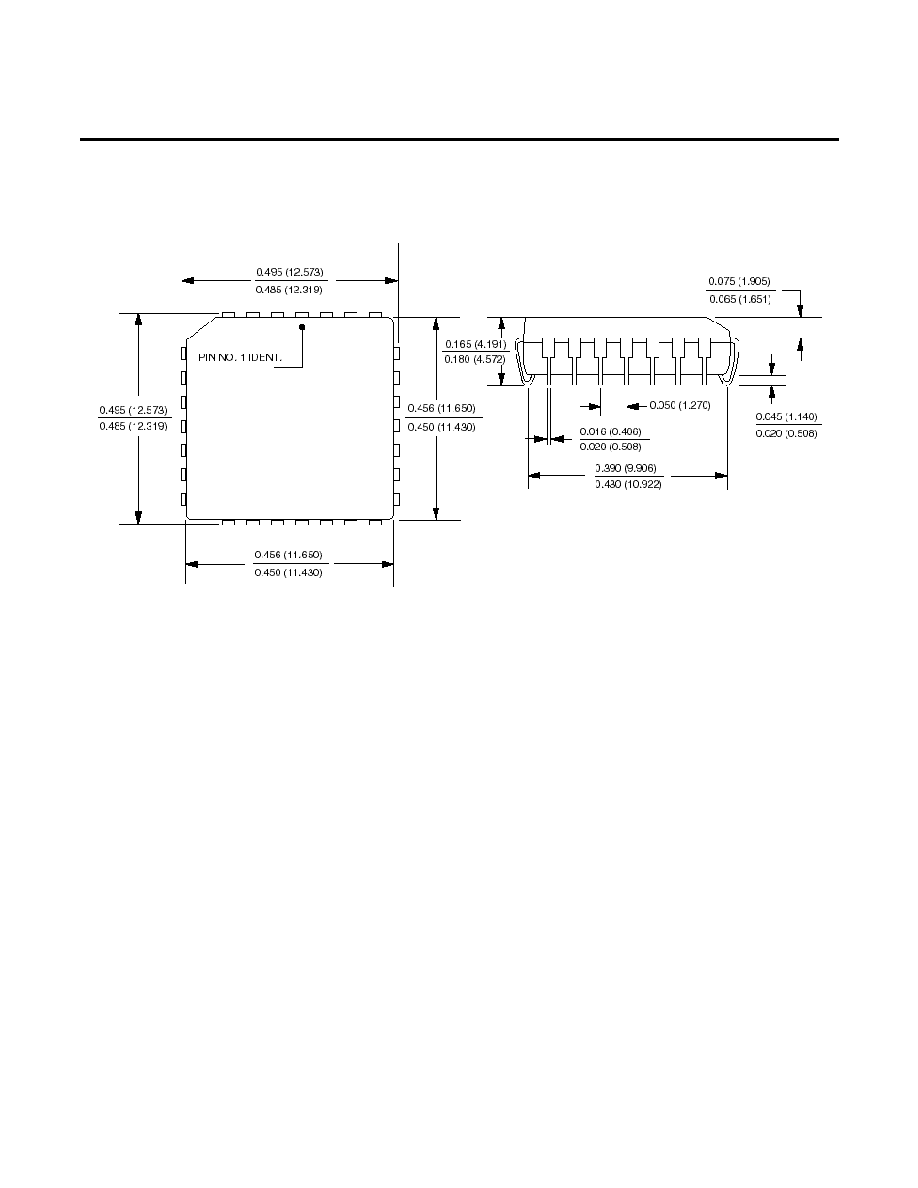
PACKAGE INFORMATION
MECHANICAL SPECIFICATIONS
28-pin PLCC
Mechanical Specification
78P2341JAT
E3/DS3/STS-1 LIU
with Jitter Attenuator
- 34 -
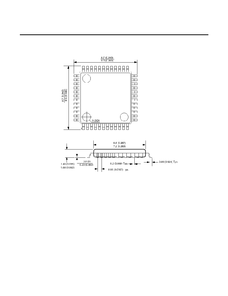
PACKAGE INFORMATION
MECHANICAL SPECIFICATIONS
48-pin TQFP (JEDEC LQFP)
Mechanical Specification

78P2341JAT
E3/DS3/STS-1 LIU
with Jitter Attenuator
- 35 -
PACKAGE INFORMATION
PIN-OUT
(Top View)
5
6
7
8
9
10
11
4
3
2
1
28 27 26
12 13 14 15 16 17 18
25
24
23
22
21
20
19
SC
K
LI
NN
GND
LI
NP
LPBK
LO
S
VC
CD
LBO
MSL0
TP
OS
TNEG
TCL
K
VC
C
T
XEN
SDIO
GND
VCC
GND
LOUTP
ICKP
LOUTN
RPOS
RNEG
RCLK
GNDD
MON
ENDEC
CKREF
78P2341
28-pin PLCC

78P2341JAT
E3/DS3/STS-1 LIU
with Jitter Attenuator
- 36 -
PACKAGE INFORMATION
PIN-OUT
(Top View)
RNEG
1
N/C
3
RCLK
2
SDIO
4
GND
5
GND
6
VCC
7
GND
8
M
S
L
0
1
7
T
P
O
S
1
8
T
N
E
G
1
9
T
C
L
K
2
0
N
/
C
2
1
V
C
C
2
2
V
C
C
2
3
T
X
E
N
2
4
4
7
S
C
K
4
8
N
/
C
4
6
G
N
D
4
5
G
N
D
4
4
L
I
N
N
4
3
G
N
D
4
2
L
I
N
P
4
1
N
/
C
4
0
L
P
B
K
3
8
V
C
C
D
3
7
V
C
C
D
36
JAERR
CKREF
34
35
RPOS
33
GNDD
32
GNDD
31
TXOK
30
N/C
29
MON
78P2341
LOUTN
1
3
POR
1
4
L
B
O
1
5
N
/
C
1
6
GND
9
10
LOUTP
11
ICKP
12
N
/
C
28
27
N/C
26
N
/
C
25
ENDEC
3
9
L
O
S
VCC
ORDERING INFORMATION
PART DESCRIPTION
ORDER NUMBER
PACKAGE MARK
48-pin JEDEC LQFP
78P2341JAT-IGT 78P2341J-IGT
28-pin PLCC
78P2341JAT-IH 78P2341J-IH
Tape & Reel option
append `R'
n/a
Lead-free option
append `/F'
append `/F

78P2341JAT
E3/DS3/STS-1 LIU
with Jitter Attenuator
- 37 -
REVISION HISTORY
Revision Date:
Revision Description:
June 24, 2002
Changes to 48-TQFP pinout (pins 14, 19, 23)
Additions to CKREF pin description
Corrected LPBK pin description and Intrinsic Transmit Jitter spec.
Marketing number change
August 06, 2003
Changed to Preliminary Status
Updated Receive Jitter Tolerance and Jitter Transfer graphs
Removed SGHI bit definition
Updated Internal Power on Reset description
Updated timing diagrams & e-spec table values
Changed recommended Rx / Tx termination resistor values to 75 / 402 ohm respectively
Preliminary Data Sheet:
This Preliminary Data Sheet describes a product not completely released to production. The specifications are
based on preliminary evaluations and may not be accurate. Samples of the described product are available and limited quantities can be
purchased. TDK Semiconductor Corporation should be consulted contacted for contacted to obtain the most current up-to-date information
about the product.
If and when manufactured and sold, this product is sold subject to the terms and conditions of sale supplied at the time of order
acknowledgment, including those pertaining to warranty, patent infringement and limitation of liability. TDK Semiconductor Corporation
(TSC) reserves the right to make changes in specifications at any time without notice. Accordingly, the reader is cautioned to verify that a
data sheet is current before placing orders. TSC assumes no liability for applications assistance.
TDK Semiconductor Corp., 6440 Oak Canyon Rd., Irvine, CA 92618
TEL (714) 508-8800, FAX (714) 508-8877, http://www.tdksemiconductor.com
©
2003 TDK Semiconductor Corporation
08/06/03 ≠ rev 1.3