78P2351
Single Channel
OC-3/ STM1-E/ E4 LIU
TARGET DATASHEET
1
APRIL 2003
DESCRIPTION
The 78P2351 is TDK's second generation LIU for
155 Mbit/s SDH/SONET (OC-3, STS-3, or STM-1)
and 140Mbit/s PDH (E4) applications. The device is
a single chip solution that includes an integrated
CDR in the transmit path for flexible NRZ to CMI
conversion. The device can interface to 75
coaxial
cable using CMI coding or directly to a fiber optics
module using NRZ coding. The 78P2351 is
compliant with all respective ANSI, ITU-T, and
Telcordia standards for jitter tolerance, generation,
and transfer.
APPLICATIONS
∑
Central Office Interconnects
∑
DSLAMs
∑
Add Drop Multiplexers (ADMs)
∑
PDH/SDH test equipment
FEATURES
∑
G.703 compliant line interface for 139.264 Mbps
or 155.52 Mbps CMI-coded coax transmission.
∑
LVPECL compatible line interface for 155.52
Mbps NRZ-coded fiber applications.
∑
Integrated adaptive CMI equalizer and CDR in
receive path.
∑
Serial, LVPECL-compatible system interface
with integrated CDR in transmit path for NRZ to
CMI conversion.
∑
4-bit parallel CMOS system interface with
master/slave Tx clock modes.
∑
Configurable via HW control pins or 4-wire µP
interface
∑
Operates from a single reference clock input.
∑
Compliant with ANSI T1.105.03-1994; ITU-T
G.751, G.813, G.823, G.825, G.958; and
Telcordia GR-253-CORE for jitter performance.
∑
Provides Loss of Lock (LOL), CMI Line Code
Violation (LCV), and G.775 compliant Loss of
Signal (LOS) detection.
∑
Receive and Transmit Monitor Modes
∑
Operates from a single 3.3V supply
∑
100-pin TQFP (JEDEC LQFP) package
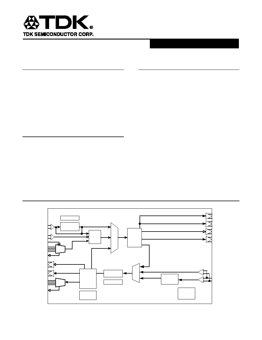
BLOCK DIAGRAM
Rx CDR
Adaptive
Eq.
CMI
Decoder
RXP/N
SODP/N
SOCKP/N
G.775
LOS
Detect
PO[3:0]D
POCK
CMI-LCV
Detect
PTOCK
PI[3:0]D
PICK
SICKP/N
SIDP/N
FIFO
Tx CDR
Lock Detect
CMI
Encoder
ECLP/N
Lock Detect
TXCKP/N
CMIP/N
CMI2P/N

78P2351 Single Channel OC-3/STM1-E/E4 Line Interface Unit
2
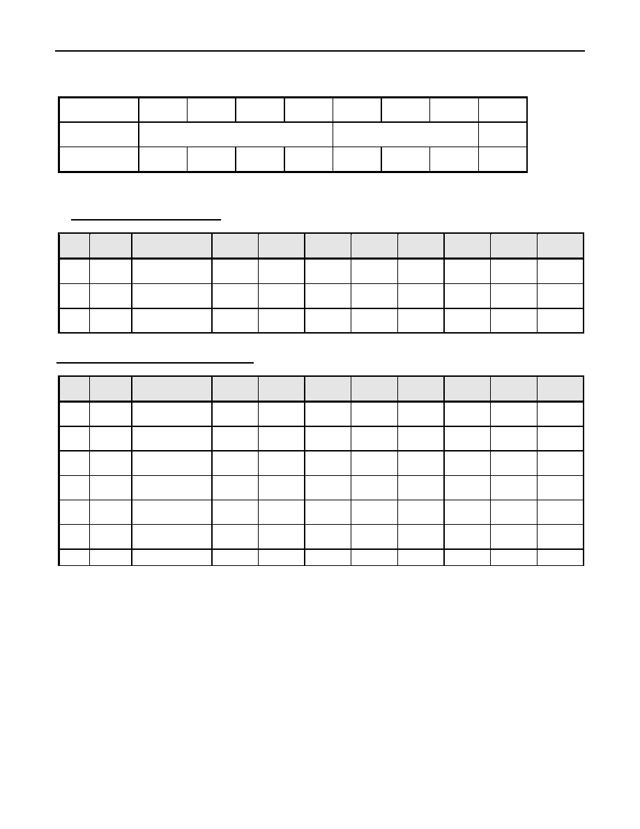
TABLE OF CONTENTS
2
FUNCTIONAL DESCRIPTION
4
MODE SELECTION
4
REFERENCE CLOCK
4
RECEIVER OPERATION
4
Receiver Monitor Mode
4
Loss of Signal / Loss of Lock
4
TRANSMITTER OPERATION
5
Serial Modes
5
Parallel Modes
6
Transmit Driver
6
Transmit Monitor Mode
6
Clock Synthesizer
6
POWER-DOWN FUNCTION
6
LOOPBACK MODES
7
POWER-ON RESET
7
SERIAL CONTROL INTERFACE
7
PROGRAMMABLE INTERRUPTS
7
REGISTER DESCRIPTION
8
REGISTER ADDRESSING
8
REGISTER TABLE
8
LEGEND
9
GLOBAL REGISTERS
9
ADDRESS 0-0: MASTER CONTROL REGISTER
9
ADDRESS 0-1: INTERRUPT CONTROL REGISTER
10
ADDRESS 0-2: I/O CONTROL REGISTER
10
PORT-SPECIFIC REGISTERS 11
ADDRESS 1-0: MODE CONTROL REGISTER
11
ADDRESS 1-1: SIGNAL CONTROL REGISTER
12
ADDRESS 1-2: ADVANCED CONTROL REGISTER 1
12
ADDRESS 1-3: ADVANCED CONTROL REGISTER 2
12
ADDRESS 1-4: MODE CONTROL REGISTER 2
13
ADDRESS 1-5: STATUS MONITOR REGISTER
13
PIN DESCRIPTION
14
LEGEND
14
TRANSMITTER PINS
14
RECEIVER PINS
15
REFERENCE AND STATUS PINS
15
CONTROL PINS
16
SERIAL-PORT PINS
17
POWER AND GROUND PINS
17

78P2351 Single Channel OC-3/STM1-E/E4 Line Interface Unit
3
TABLE OF CONTENTS
(continued)
ELECTRICAL SPECIFICATIONS
18
ABSOLUTE MAXIMUM RATINGS
18
RECOMMENDED OPERATING CONDITIONS
18
DC CHARACTERISTICS
18
ANALOG PINS CHARACTERISTICS
19
DIGITAL I/O CHARACTERISTICS
19
Pins of type CI, CIU, CID 19
Pins of type CIS
19
Pins of type CO and COZ 19
Pins of type PO
19
SERIAL-PORT TIMING CHARACTERISTICS
20
TRANSMITTER TIMING CHARACTERISTICS
21
TIMING DIAGRAM: Transmitter Waveforms
21
REFERENCE CLOCK CHARACTERISTICS
22
RECEIVER TIMING CHARACTERISTICS
22
TIMING DIAGRAM: Receive Waveforms
22
TRANSMITTER SPECIFICATIONS FOR CMI INTERFACE
23
TRANSMITTER OUTPUT JITTER
28
RECEIVER (Transformer-coupled)
29
RECEIVER SPECIFICATIONS FOR CMI INTERFACE
29
RECEIVER JITTER TOLERANCE
30
RECEIVER JITTER TRANSFER FUNCTION
32
CMI Mode Loss of Signal Condition
33
APPLICATION INFORMATION
34
EXTERNAL COMPONENTS
34
TRANSFORMER SPECIFICATIONS
34
RECOMMENDED LVPECL TERMINATIONS
34
MECHANICAL SPECIFICATIONS
35
PACKAGE INFORMATION
36
Revision History
37
78P2351 Single Channel OC-3/STM1-E/E4 Line Interface Unit
4
FUNCTIONAL DESCRIPTION
The 78P2351 contains all the necessary transmit
and receive circuitry for connection between
139.264Mbit/s and 155.52Mbit/s signals and the
digital universe.
The chip is controllable through pins or serial port
register settings. In hardware mode (pin control) the
SPSL pin must be low. In software mode (SPSL pin
high), control pins are disabled and the 78P2351
must be configured via the 4-wire serial port.
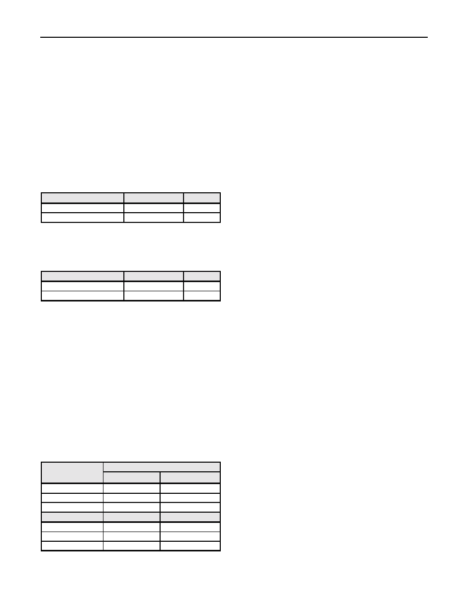
MODE SELECTION
The SDO_E4 pin or E4 register bit determines which
rate the device operates in according to the table
below. This control combined with CKSL also
selects the global reference frequency.
Rate
SDO_E4 pin
E4 bit
E4 High
1
STM-1, STS-3, OC-3
Low
0
The SEN_CMI pin or CMI register bit selects one of
two media for reception and transmission: coaxial
cable in CMI mode or optical fiber in ECL (NRZ)
mode.
Media (coding)
SEN_CMI pin
CMI bit
75 ohm Coax (CMI)
High
1
Fiber (NRZ)
Low
0
The SDI_PAR pin or PAR register bit selects the
interface to the framer to be four bit parallel or serial.
For each interface there are different clocking
schemes for the transmitter. These modes and
their controls are described in the TRANSMITTER
OPERATION section.
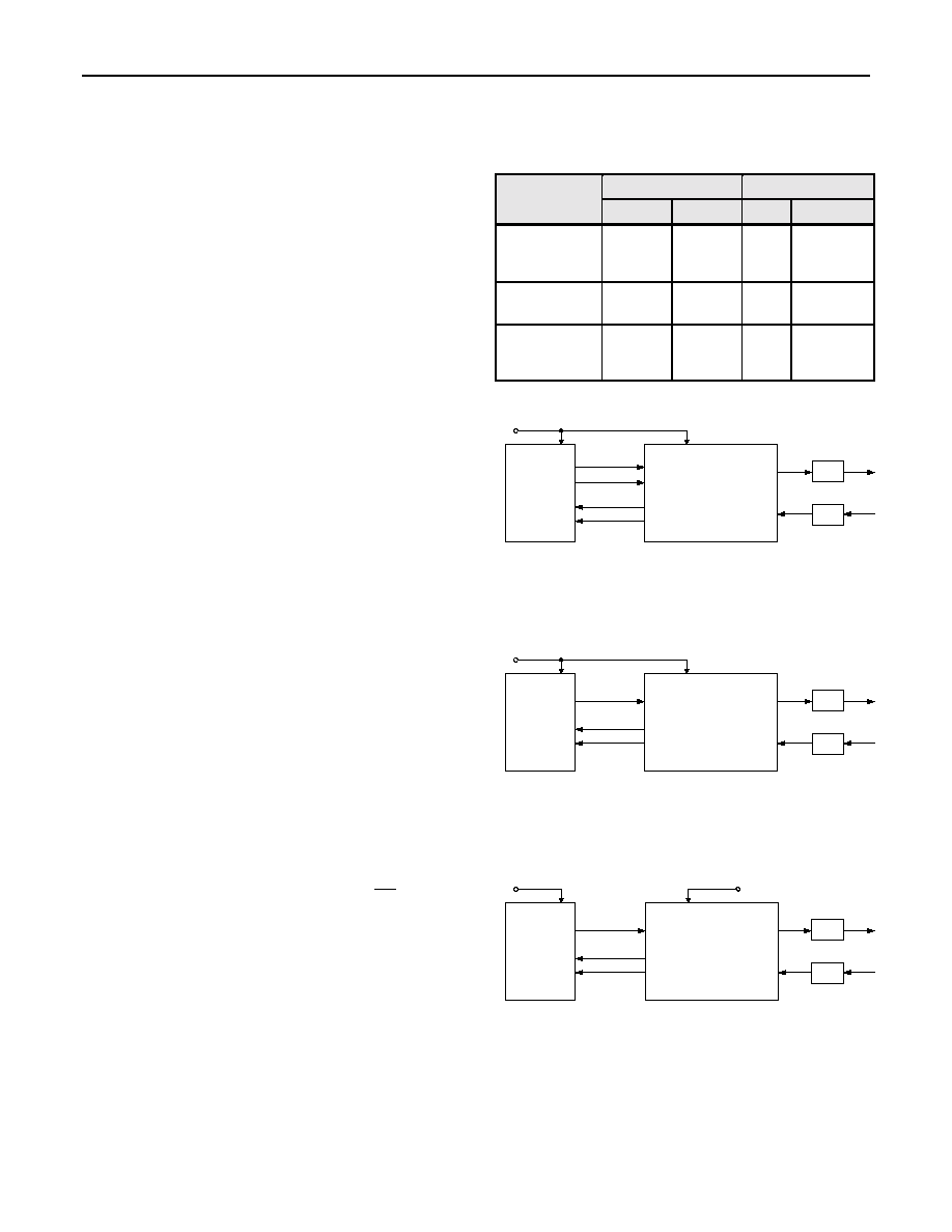
REFERENCE CLOCK
The 78P2351 requires a reference clock supplied to
the CKREFP/N pins. For reference frequencies of
77.76MHz or lower, the device accepts a single
ended CMOS input at CKREFP. For reference
frequencies of 139.264/155.52MHz, the device
accepts a differential clock input at CKREFP/N. The
frequency of this reference input is selected by the
rate selection and the CKSL control pin or register
bit.
Reference Frequency
CKSL pin
SDO_E4 low
SDO_E4 high
Low 19.44MHz
17.408MHz
Float 77.76MHz
N/A
High 155.52MHz
139.264MHz
CKSL[1:0] bits
E4 bit = 0
E4 bit = 1
0 0
19.44MHz
17.408MHz
1 0
77.76MHz
N/A
1 1
155.52MHz
139.264MHz
RECEIVER OPERATION
The receiver accepts serial data, at 155.52Mbit/s or
139.264Mbit/s from the RXP/N inputs. In CMI mode,
the CMI-coded inputs come from a coaxial cable that
is transformer-coupled to the chip. In ECL (NRZ)
mode, the input pins receive NRZ LVPECL level
signals from an O/E converter.
The CMI signal first enters an AGC, which has a
selectable gain range setting. When Receiver
Monitor Mode is enabled, the AGC can compensate
for a monitor signal with 16 to 20 dB of flat loss. The
signal then enters a high performance adaptive
equalizer designed to overcome inter-symbol
interference caused by long cable. The variable
gain differential amplifier automatically controls the
gain to maintain a constant voltage level output
regardless of the input voltage level. In ECL (NRZ)
mode, the input signals bypass the adaptive
equalizer.
The outputs of the data comparators are connected
to the clock recovery circuits. The clock recovery
system employs a digital PLL, which uses a
reference frequency derived from the clock applied
to the CKREFP/N pins.
After the clock and data have been recovered, the
data is converted to binary by the CMI to binary
decoder. The
CMI Line Code Violation (LCV
)
detector will flag code errors while the decoder
continues to function normally. The three conditions
that will flag a LCV are:
∑
`0' has a falling transition mid-bit instead of a
rising transition
∑
A high `1' is recovered when it should have
been a low `1'
∑
A low `1' is recovered when it should have
been a high `1'
In serial mode, the clock and data are transmitted
through the LVPECL drivers. In parallel mode, the
data is converted into four bit parallel segments
before being transmitted through the CMOS drivers.
Receiver Monitor Mode
The SCK_MON pin or MON register bit puts the
receiver in monitor mode and adds 20dB of flat gain
to the receive signal before equalization. Receiver
Monitor Mode is available in CMI mode only.
Loss of Signal / Loss of Lock
The 78P2351 includes standards compliant Loss of
Signal (LOS) and Loss of Lock (LOL) indicators for
the receive signal. During LOS conditions, the
receive data outputs are squelched while the receive
clock outputs a line rate clock generated from the
reference clock input. The LOS indicator is intended
for electrical CMI interfaces only.
78P2351 Single Channel OC-3/STM1-E/E4 Line Interface Unit
5
TRANSMITTER OPERATION
The transmitter section generates an analog signal
for transmission through either a transformer onto
the coaxial cable or directly to a fiber optics module.
The 78P2351 provides a flexible system interface for
compatibility with most off-the-shelf framers and
custom ASICs. The device supports a 4-bit parallel
interface in either slave or master clocking modes
and a number of serial NRZ modes.
Serial Modes
In
Figure 1
, serial NRZ data is input to the 78P2351
on the SIDP/N pins at LVPECL levels. The data is
latched in on the rising edge of SICKP/N. A clock
decoupling FIFO is provided to decouple the on chip
and off chip clocks. The SICKP/N clock provided by
the framer/mapper IC should be source synchronous
with the internal reference transmit clock if the FIFO
is to be used. Since both clocks go through different
delay paths, it is inevitable that the phase
relationship between the two clocks can vary in a
bounded manner due to the fact that the absolute
delays in the two paths can vary over time. The
FIFO is designed to allow long-term clock phase drift
not exceeding +/- 25.6ns to be handled without
transmit error. If the clock wander exceeds the
specified limits, the FIFO will over or under flow, and
the FERR register signal will be asserted. The FIFO
is then automatically re-centered. This signal can be
used to trigger an interrupt. This interrupt event is
cleared when an FRST pulse is applied, and the
FIFO is re-centered.
If no serial transmit clock is available, as in
Figure 2
,
the 78P2351 will recover a clock from the serial NRZ
data input and pass the data through the FIFO. In
this mode, the NRZ data should be source
synchronous with the reference clock applied at
CKREFP/N. The transmitter also includes a Loss of
Lock indicator (TXLOL) which can be used to trigger
and interrupt. Note that the FIFO is automatically re-
centered when the TXLOL register bit transitions
from high to low.
Figure 3
represents the condition where no serial
transmit clock is available and the data is not source
synchronous to the reference clock input. In this
mode, the 78P2351 will recover a clock from the
serial plesiochronous data and bypass the FIFO.
Each of the described transmit serial modes can be
configured in HW mode and SW mode as shown in
the table below:
HW Control Pins SW Control Bits
Serial Mode
SDI_PAR CKMODE PAR
SMOD[1:0]
Synchronous
clock + data
(CDR bypass)
Low Low 0 0
0
Synchronous
data
Low Floating
0 1
0
Plesiochronous
data
(FIFO bypass)
Low High 0 0
1
TDK
78P2351
Framer/
Mapper
NRZ
NRZ
140 / 155 MHz
Reference
Clock
SODP/N
SOCKP/N
SIDP/N
CKREFP/N
RXP/N
CMIP/N
XFMR
XFMR
CMI
CMI
Coax
Coax
140 / 155 MHz
SICKP/N
Figure 1: Synchronous; clock and data available
(Tx CDR bypassed, FIFO enabled)
TDK
78P2351
Framer/
Mapper
NRZ
NRZ
140 / 155 MHz
Reference
Clock
SODP/N
SOCKP/N
SIDP/N
CKREFP/N
RXP/N
CMIP/N
XFMR
XFMR
CMI
CMI
Coax
Coax
Figure 2: Synchronous; data only
(Tx CDR enabled, FIFO enabled)
TDK
78P2351
Framer/
Mapper
NRZ
NRZ
140 / 155 MHz
Reference
Clock
Reference
Clock
SODP/N
SOCKP/N
SIDP/N
CKREFP/N
RXP/N
CMIP/N
XFMR
XFMR
CMI
CMI
Coax
Coax
Figure 3: Plesiochronous; data only
(Tx CDR enabled, FIFO bypassed)

78P2351 Single Channel OC-3/STM1-E/E4 Line Interface Unit
6
Parallel Modes
In parallel modes, 4-bit CMOS data segments are
input to the chip with a 38.88MHz clock. These
inputs are passed to the 4x8 decoupling FIFO and
then to a serializer for transmission. For maximum
compatibility, the 78P2351 can operate in both slave
and master clock modes as shown in Figures 4, 5
respectively..
HW Control Pins
SW Control Bits
Parallel
Mode
SDI_PAR CKMODE
PAR
PMODE
Slave
High Low/Float
1
0
Master
High High
1
1
4-bit CMOS TTL
4-bit CMOS TTL
TDK
78P2351
Framer/
Mapper
Reference
Clock
CKREFP/N
RXP/N
CMIP/N
XFMR
XFMR
CMI
CMI
Coax
Coax
PO[3:0]D
POCK
PIxCK
PI[3:0]D
34/39 MHz
34/39 MHz
Figure 4: Slave Parallel Mode
4-bit CMOS TTL
4-bit CMOS TTL
TDK
78P2351
Framer/
Mapper
Reference
Clock
CKREFP/N
RXP/N
CMIP/N
XFMR
XFMR
CMI
CMI
Coax
Coax
PO[3:0]D
POCK
PTOCK
PI[3:0]D
34/39 MHz
34/39 MHz
Figure 5: Master Parallel Mode
Transmit Driver
When the CMI pin is high, the chip is in CMI mode
and a 75
coaxial cable is used as the transmission
medium. In this mode, the CMIP/N pins connect the
chip to the coaxial cable through a transformer and
termination resistors. In CMI mode, the transmitter
shapes the transmit pulses to meet the appropriate
template. Advanced peaking and amplitude controls
are also available in both HW and SW modes to
accommodate for less than ideal board conditions
When the CMI pin is low, the chip is in ECL (NRZ)
mode. The output data signal from the ECLP/N pins
have LVPECL levels and interface directly to a fiber
module. The CMI driver, encoder and decoder are
disabled in ECL (NRZ) mode.
A 2x line rate clock is also available at the TXCKP/N
pins for downstream synchronization or interfacing
to equipment lacking integrated clock recovery.
Transmit Monitor Mode
An optional redundant transmit output is available in
CMI mode for transmit monitoring. These outputs
(CMI2P/N) are activated when the RCSL pin or
RCSL register bit is activated.
TDK
78P2351
RXP/N
CMIP/N
XFMR
XFMR
CMI
CMI
Coax
Coax
CMI2P/N
XFMR
CMI
Coax
Figure 6: Transmit Monitor Output
Clock Synthesizer
The transmitter clock synthesizer is a low-jitter PLL
that generates a 311.04MHz (278.528MHz) clock for
the CMI encoder. A synthesized line rate reference
clock is also used in both the receive and transmit
sides.
POWER-DOWN FUNCTION
Power-down control is provided to allow the
78P2351 to be shut off. Transmit and receive
power-down can be set independently through SW
control. Global power-down is achieved by
powering down both the transmitter and receiver.
Note the serial interface and Configuration Registers
are not affected by power-down.
In HW mode, the transmitter can be powered down
using the TXPD control pin.
78P2351 Single Channel OC-3/STM1-E/E4 Line Interface Unit
7
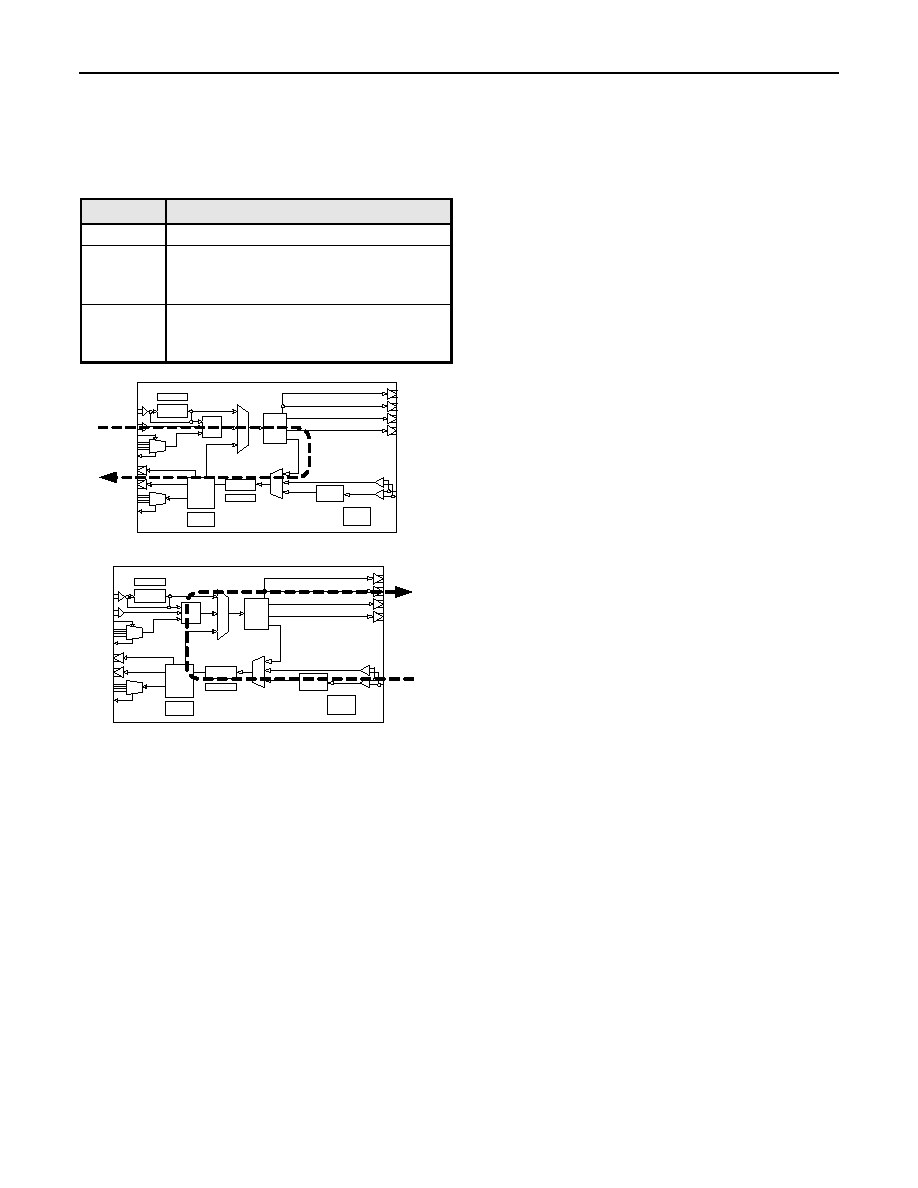
LOOPBACK MODES
In SW mode, LLBK and RLBK bits are provided to
activate the local and remote loopback modes
respectively. In HW mode, the LPBK pin can be
used to activate local and remote loopback modes
as shown below.
LPBK pin Loopback Mode
Low Normal
operation
Float
Remote (digital) Loopback:
Recovered receive clock and data
looped back to transmitter
High
Local (analog) Loopback:
Transmit clock and data looped back to
receiver
Rx CDR
Adaptive
Eq.
CMI
Decoder
RXP/N
SODP/N
SOCKP/N
G.775
LOS
Detect
PO[3:0]D
POCK
CMI-LCV
Detect
PTOCK
PI[3:0]D
PICK
SICKP/N
SIDP/N
FIFO
Tx CDR
Lock Detect
CMI
Encoder
ECLP/N
Lock Detect
TXCKP/N
CMIP/N
CMI2P/N
Figure 7: Local (Analog) Loopback
Rx CDR
Adaptive
Eq.
CMI
Decoder
RXP/N
SODP/N
SOCKP/N
G.775
LOS
Detect
PO[3:0]D
POCK
CMI-LCV
Detect
PTOCK
PI[3:0]D
PICK
SICKP/N
SIDP/N
FIFO
Tx CDR
Lock Detect
CMI
Encoder
ECLP/N
Lock Detect
TXCKP/N
CMIP/N
CMI2P/N
Figure 8: Remote (Digital) Loopback
POWER-ON RESET
Power-On Reset (POR) function is provided on chip.
Upon initial power-up, a reset pulse is internally
generated. This resets all registers to their default
values as well as all state machines within the
transceiver to known initial values. The reset signal
is also brought out to the
POR pin. The POR pin is
a special function pin that allows for the following:
∑
Override the internal
POR signal by driving in
an external
POR signal;
∑
Use the
POR signal to drive other IC's power-
on reset;
∑
Add external capacitor to slow down the
release of power-on reset (approximately 8
µ
s
per nF added).
The internal resistance of the
POR pin is
approximately 5k
.
SERIAL CONTROL INTERFACE
The serial port controlled register allows a generic
controller to interface with the 78P2351. It is used
for mode settings, diagnostics and test, retrieval of
status and performance information, and for on-chip
trimming. The SPSL pin must be high in order to
use the serial port.
The serial interface consists of four pins: Serial Port
Enable (SEN_CMI), Serial Clock (SCK_MON), Serial
Data In (SDI_PAR), and Serial Data Out (SDO_E4).
The SEN_CMI pin initiates the read and write
operations. It can also be used to select a particular
device allowing SCK_MON, SDI_PAR and SDO_E4
to be bussed together. SCK_MON is the clock input
that times the data on SDI_PAR and SDO_E4. Data
on SDI_PAR is latched in on the rising-edge of
SCK_MON, and data on SDO_E4 is clocked out
using the falling edge of SCK_MON.
SDI_PAR is used to insert mode, address, and
register data into the chip. Address and Data
information are input least significant bit (LSB) first.
The mode and address bit assignment and register
table are shown in the following section.
SDO_E4 is a tristate capable output. It is used to
output register data during a read operation.
SDO_E4 output is normally high impedance, and is
enabled only during the duration when register data
is being clocked out. Read data is clocked out least
significant bit (LSB) first.
If SDI_PAR coming out of the micro-controller chip is
also tristate capable, SDI_PAR and SDO_E4 can be
connected together to simplify connections.
The maximum clock frequency for register access is
20MHz.
PROGRAMMABLE INTERRUPTS
In addition to the receiver LOS and LOL status pins,
the 78P2351 provides a programmable interrupt for
both the transmitter and receiver. In HW control
mode, the default functions of each interrupt is as
follows:
∑
INTTX = Transmit Loss of Lock (TXLOL) or
FIFO error (FERR)
∑
INTRX = CMI Line Code Violation
(CMIERR)
78P2351 Single Channel OC-3/STM1-E/E4 Line Interface Unit
8
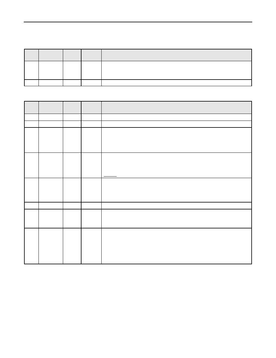
REGISTER DESCRIPTION
REGISTER ADDRESSING
Address Bits
Bit 7
Bit 6
Bit 5
Bit 4
Bit 3
Bit 2
Bit 1
Bit 0
Port
Address Sub-Address
Read/
Write
Assignment
PA[3] PA[2] PA[1] PA[0] SA[2] SA[1] SA[0] R/W*
REGISTER TABLE
a) PA[3:0] = 0 : Global Registers
Sub
Addr
Reg.
Name
Description
Bit 7
Bit 6
Bit 5
Bit 4
Bit 3
Bit 2
Bit 1
Bit 0
0 MSCR
(R/W)
Master Control
E4
<0>
-- PAR
<0>
CKSL[1]
<X>
CKSL[0]
<X>
-- --
SRST
<0>
1 INTC
(R/W)
Interrupt Control
INPOL
<0>
-- MCERR
<1>
MRLOS
<0>
MRLOL
<0>
--
MTLOL
<1>
MFERR
<1>
2 IOCR
(R/W)
I/O
Control
-- -- -- -- -- -- --
RCSL
<0>
b) PA[3:0] = 1 : Port-Specific Registers
Sub
Addr
Reg.
Name
Description
Bit 7
Bit 6
Bit 5
Bit 4
Bit 3
Bit 2
Bit 1
Bit 0
0 MDCR
(R/W)
Mode Control
PDTX
<0>
PDRX
<0>
PMODE
<X>
SMOD[1]
<X>
SMOD[0]
<X>
MON
<0>
-- --
1 SGCR
(R/W)
Signal
Control -- -- --
RLBK
<0>
LLBK
<0>
RCLKP
<0>
TCLKP
<0>
FRST
<0>
2 ACR1
(R/W)
Advanced
Control 1
--
--
-- -- -- --
TPK
<0>
DU
<0>
3
ACR2
(R/W)
Advanced
Control 2
-- -- -- -- --
BST[1]
<0>
BST[0]
<0>
--
4 MCR2
(R/W)
Mode Control 2
CMI
<1>
-- -- -- -- -- -- --
5 STAT
(R/C)
Status Monitor
--
--
CMIERR
<X>
RXLOS
<X>
RXLOL
<X>
-- TXLOL
<X>
FERR
<X>
6-7
--
Reserved
-- -- -- -- -- -- -- --

78P2351 Single Channel OC-3/STM1-E/E4 Line Interface Unit
9
REGISTER DESCRIPTION
(continued)
LEGEND
TYPE DESCRIPTION
TYPE DESCRIPTION
R/O
Read only
R/W
Read or Write
R/C Read
and
Clear
GLOBAL REGISTERS
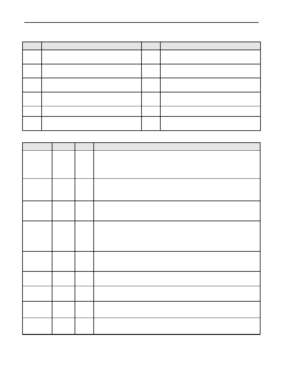
ADDRESS 0-0: MASTER CONTROL REGISTER
BIT
NAME
TYPE
DFLT
VALUE
DESCRIPTION
7 E4
R/W 0
Line Rate Selection:
Selects the line rate of all channels as well as the input clock frequency at the
CKREFP/N pins.
0: OC-3, STS-3, STM-1 (155.52MHz)
1: E4 (139.264MHz)
6 -- R/W 0
Unused
5 PAR R/W 0
Serial/Parallel Selection:
Selects the interface to the framer.
0: Serial
1: Parallel
4:3
CKSL
[1:0]
R/W X
Reference Clock Frequency Selection:
Selects the reference clock frequency input at CKREFP/N pins. Secondary
values correspond to E4 frequencies. Default values depend on the pin
selection upon reset.
11: 155.52MHz / 139.264MHz
10: 77.76MHz / NA
00: 19.44MHz / 17.408MHz
2:1 -- R/W 0 Unused
0 SRST R/W 0
Register Soft-Reset:
When this bit is set, all registers are reset to their default values. This register
bit is self-clearing.
78P2351 Single Channel OC-3/STM1-E/E4 Line Interface Unit
10
REGISTER DESCRIPTION
(continued)
ADDRESS 0-1: INTERRUPT CONTROL REGISTER
This register selects the events that would cause the interrupt pins to be activated. User may set as many bits as
required.
BIT
NAME
TYPE
DFLT
VALUE
DESCRIPTION
7 INPOL R/W 0
Interrupt Pin Polarity Selection:
0 : Interrupt output is active-low
1 : Interrupt output is active-high
6 -- R/W 0
Reserved
5 MCERR R/W 1
Receive CMI Code Error Mask (active low):
Gates the respective RXCER register bit to the
INTRX interrupt pin.
0: Mask
1: Pass
4 MRLOS R/W 0
Receive Loss of Signal Error Mask (active low):
Gates the respective RXLOS register bit to the
INTRX interrupt pin.
0: Mask
1: Pass
3 MRLOL R/W 0
Receive Loss of Lock Error Mask (active low):
Gates the respective RXLOL register bit to the
INTRX interrupt pin.
0: Mask
1: Pass
2 -- R/W 0
Unused
1 MTLOL R/W 1
TXLOL Error Mask (active low):
Gates the TXLOL register bit to the
INTTX interrupt pin.
0: Mask
1: Pass
0 MFERR R/W 1
FIERR Error Mask (active low):
Gates the respective FIERR register bit to the
INTTX interrupt pin.
0: Mask
1: Pass
ADDRESS 0-2: I/O CONTROL REGISTER
BIT
NAME
TYPE
DFLT
VALUE
DESCRIPTION
7:1 -- R/W 0 Unused
0 RCSL R/W 0
Redundant Channel Enable:
Enables transmit monitor outputs at CMI2P/N pins.
0: Disable
1: Enable

78P2351 Single Channel OC-3/STM1-E/E4 Line Interface Unit
11
REGISTER DESCRIPTION
(continued)
PORT-SPECIFIC REGISTERS
For PA[3:0] = 1 only. Accessing a register with port address greater than 1 constitutes an invalid command, and
the read/write operation will be ignored.
ADDRESS 1-0: MODE CONTROL REGISTER
BIT
NAME
TYPE
DFLT
VALUE
DESCRIPTION
7 PDTX R/W 0
Transmitter Power-Down:
0 : Normal Operation
1 : Power-Down
6 PDRX R/W 0
Receiver Power-Down:
0 : Normal Operation
1 : Power-Down
5 PMODE R/W X
Parallel Mode Interface Selection:
When PAR=1 (Master Control Regsiter: bit 5), PMODE selects the source
of the transmit parallel input clock, either taken from the framer externally
or generated internally.
0: Parallel clock is taken as an input to the transmitter
1: Parallel clock is given as an output from the transmitter
4 SMOD[1] R/W
X
3 SMOD[0] R/W
X
Serial Mode Interface Selection:
When PAR=0 (Master Control Regsiter: bit 5), SMOD[1:0] configures the
transmitter's system interface.
SMOD[1] SMOD[0]
0 0 Synchronous clock and data are passed through a
FIFO. The CDR is bypassed.
1 0 Synchronous data is passed through the CDR and
then through the FIFO.
0 1 Plesiochronous data is passed through the CDR to
recover a clock, but the FIFO is bypassed because
the data is not synchronous with the reference clock.
1 1 Loop Timing Mode Enable: The recovered receive
clock is used as the reference for the transmit section.
The transmit data is passed through the CDR, but the
FIFO is bypassed.
2 MON R/W 0
Receive Monitor Mode Enable:
0: Normal Operation
1: When Adds 20dB of flat gain to the receive signal before equalization.
NOTE: Monitor mode is only available in CMI mode.
1 -- R/W 0
Reserved
0 -- R/W 1
Reserved

78P2351 Single Channel OC-3/STM1-E/E4 Line Interface Unit
12
REGISTER DESCRIPTION
(continued)
ADDRESS 1-1: SIGNAL CONTROL REGISTER
BIT
NAME
TYPE
DFLT
VALUE
DESCRIPTION
7:5 -- R/W 0 Reserved
4 RLBK R/W 0
3 LLBK R/W 0
Loopback Selection:
RLBK LLBK
0 0 Normal operation
1 0 Remote Loopback Enable: Recovered receive data
and clock are looped back to the transmitter for
retransmission. Valid for both parallel and serial
modes.
0 1 Local Loopback Enable: The serial transmit data is
looped back and used as the input to the receiver.
2 RCLKP R/W 0
Receive Clock Inversion Select:
This bit will invert the receive output clock.
0: Normal
1: Invert
1 TCLKP R/W 0
Transmit Clock Inversion Select:
This bit will invert the transmit input system clock.
0: Normal
1: Invert
0 FRST R/W 0
FIFO Reset:
0: Normal operation
1: Reset FIFO pointers to default locations.
NOTE: Transmit monitor port will also be affected by FRST
ADDRESS 1-2: ADVANCED CONTROL REGISTER 1
BIT
NAME
TYPE
DFLT
VALUE
DESCRIPTION
7:2 -- R/W 0 Reserved
1 TPK R/W 0 Transmit Driver Peaking Enable:
TBD
0 DU R/W 0 Transmit Driver Reverse Peaking Enable:
TBD
ADDRESS 1-3: ADVANCED CONTROL REGISTER 2
BIT
NAME
TYPE
DFLT
VALUE
DESCRIPTION
7:3 ---- R/W
10101
Reserved
2:1 BST[1:0] R/W 00 Transmit Driver Amplitude Boost:
TBD
0 ---- R/W 0
Reserved
78P2351 Single Channel OC-3/STM1-E/E4 Line Interface Unit
13
REGISTER DESCRIPTION
(continued)
ADDRESS 1-4: MODE CONTROL REGISTER 2
BIT
NAME
TYPE
DFLT
VALUE
DESCRIPTION
7 CMI R/W 1
Line Interface Mode Selection:
0: Optical (LVPECL)
1: Coaxial cable (CMI encoded)
6:0 -- R/W 0
Reserved
ADDRESS 1-5: STATUS MONITOR REGISTER
BIT
NAME
TYPE
DFLT
VALUE
DESCRIPTION
7 -- R/C
X
Unused
6 -- R/C
X
Reserved
5 CMIERR R/C X
Receive CMI Coding Error Indication:
This bit is set when the recovered receive CMI data is incorrectly coded.
0: Normal operation
1: CMI code error detected
4 RXLOS R/C X
Loss of Signal Indication:
0: Normal operation
1: Loss of signal condition detected
NOTE: RXLOS is intended for CMI mode only.
3 RXLOL R/C X
Receive Loss of Lock Indication:
0: Normal operation
1: Recovered receive clock frequency differs from the reference by more
than +/- 1000ppm.
2 -- R/C
X
Unused
1 TXLOL R/C X
Transmit Loss of Lock Indication:
0: Normal operation
1: Transmit CDR unlocked
0 FERR R/C X
Transmit FIFO Error Indication:
This bit is set whenever the internal FERR signal is asserted, indicating
that the FIFO is operating at its depth limit. It is reset to 0 when the
FRST pin is asserted.
0: Normal operation
1: Transmit FIFO phase error
78P2351 Single Channel OC-3/STM1-E/E4 Line Interface Unit
14
PIN DESCRIPTION
LEGEND
TYPE
DESCRIPTION
TYPE
DESCRIPTION
A
Analog Pin
(Tie unused pins to ground)
PO
LVPECL-Compatible Differential Output
(Tie unused pins to supply)
CIT
3-State CMOS Digital Input
CO
CMOS Digital Output
(Leave unused pins floating)
CI
CMOS Digital Input
(Tie unused pins to ground)
COZ
CMOS Tristate Digital Output
(Leave unused pins floating)
CIU
CMOS Digital Input w/ Pull-up
PI
LVPECL-Compatible Differential Input
(Tie unused pins to ground)
CID
CMOS Digital Input w/ Pull-down
S
Supply
CIS
CMOS Schmitt Trigger Input
(Tie unused pins to ground)
G Ground
TRANSMITTER PINS
NAME
PIN
TYPE DESCRIPTION
PI0D
PI1D
PI2D
PI3D
24
25
26
27
CI
Transmit Data Parallel Input:
The four bit CMOS parallel inputs are latched in on the rising edge of the
transmit parallel input clock. MSB of the data is transmitted first.
PICK
23 CI
Transmit Parallel Clock Input:
A 38.88MHz CMOS clock input that should be source synchronous with the
reference clock supplied at the CKREFP/N pins.
PTOCK
28 CO
Transmit Parallel Clock Output:
A 38.88MHz CMOS clock output that is intended to latch in synchronous
parallel data.
SIDP
SIDN
8
9
PI
Transmit Serial Data Input:
This differential input is clocked in on the rising edge of the transmit serial
input clock. If source synchronous with the reference clock, this data can be
input to a FIFO, otherwise the clock and data can be transmitted directly. A
CDR can be multiplexed in to the transmit path if no serial clock is available.
SICKP
SICKN
5
6
PI
Transmit Serial Clock Input:
A 155.52MHz synchronous differential input clock used to clock in the serial
data
CMIP
CMIN
93
94
A
Transmit Serial CMI Data Output:
A CMI encoded data signal conforming to the relevant pulse templates
CMI2P
CMI2N
79
78
A
Transmit Monitor Output:
Redundant transmit driver enabled by RCSL control.
TXCKP
TXCKN
96
97
PO
Transmit Serial Clock Output:
A 2x line rate LVPECL clock output used to clock out the transmit data
ECLP
ECLN
99
100
PO
Transmit Serial LVPECL Data Output:
Transmit NRZ data

78P2351 Single Channel OC-3/STM1-E/E4 Line Interface Unit
15
PIN DESCRIPTION
(continued)
RECEIVER PINS
NAME
PIN
TYPE DESCRIPTION
PO0D
PO1D
PO2D
PO3D
41
40
37
36
CO
Receive Data Parallel Output:
The four bit CMOS parallel outputs are clocked out on the falling edge of the
receive parallel output clock. The MSB of the output is received first.
POCK
33 CO
Receive Parallel Clock Output:
A 38.88MHz CMOS clock output generated by dividing down the recovered
receive clock. The output is multiplexed in from the divided down reference
clock whenever LOS is high.
SODP
SODN
20
21
PO
Receive Serial Data Output:
Recovered receive serial data
SOCKP
SOCKN
18
19
PO
Receive Serial Clock Output:
Recovered receive serial clock
RXP
RXN
90
91
A/
PI
Receive Serial CMI or LVPECL Input:
The input signal is either transformer coupled for CMI data or at LVPECL
levels for NRZ data
REFERENCE AND STATUS PINS
NAME
PIN
TYPE DESCRIPTION
CKREFP
CKREFN
83
82
PI
Reference Clock Input:
A differential 139.264MHz, 155.52MHz differential clock input at CKREFP/N
or a single-ended 17.408MHz, 19.44MHz, 77.78MHz CMOS clock input at
CKREFP (tie CKREFN to ground when unused).
All reference clocks are +/- 20ppm.
LOS
61 CO
Loss of Signal:
Standards compliant loss of signal indicator. To be used for electrical CMI
interfaces only.
LOL
60 CO
Loss of Lock:
This condition is met when the recovered clock frequency differs from the
reference clock frequency by more than +/- 1000ppm.
INTTX
67 CO
Transmitter Fault Interrupt Flag (active low):
When a transmitter error event occurs (as defined in the Interrupt Control
Register Description), the
INTTX pin will change state to indicate an
interrupt. The interrupt is cleared by a read to the STAT Register or issue of
a FRST FIFO reset pulse if the FIERR signal caused the interrupt. The
default interrupt condition is a loss of lock in the transmitter CDR.
INTRX
52 CO
Receiver Fault Interrupt Flag (active low):
When a receiver error event occurs (as defined in the Interrupt Control
Register Description), the
INTRX pin will change state to indicate an
interrupt. The interrupt is cleared by a read to the STAT Register. The
default interrupt condition is a CMI line code violation.
POR
64 A
Power-On Reset (active low):
See Power-On Reset description on use of this pin.
78P2351 Single Channel OC-3/STM1-E/E4 Line Interface Unit
16
PIN DESCRIPTION
(continued)
CONTROL PINS
NAME
PIN
TYPE DESCRIPTION
FRST
59 CIT
FIFO Phase-Initialization Control:
Should normally be floating or high. When asserted, the transmit FIFO
pointers are reset to the respective "centered" states. Also resets the FIERR
interrupt bit. De-assertion edge of FRST will resume FIFO operation.
∑
Low: FRST assertion.
∑
Float/High: Normal
NOTE: Transmit Monitor port is also affected during a FIFO reset.
RCSL
14 CID
Redundant Channel Selection:
Enables the redundant Transmit Monitor Output at pins CMI2P/N.
∑
Low: Normal operation (CMIP/N active only)
∑
High: Transmit Monitor Mode (CMIP/N and CMI2P/N active)
LPBK
15 CIT
Loopback Selection:
∑
Low: Normal operation
∑
Float: Remote Loopback Enable: Recovered receive data and clock
are looped back to the transmitter for retransmission.
∑
High: Local Loopback Enable: The serial transmit data is looped back
and used as the input to the receiver.
CKMODE
13 CIT
Clock Mode Selection:
In PARALLEL mode (SDI_PAR high):
∑
Low/Float: Parallel transmit clock is input to the 78P2351
∑
High: Parallel transmit clock is output from the 78P2351
In SERIAL mode (SDI_PAR low):
∑
Low: Reference clock is synchronous to transmit clock and data. Data
is passed through a FIFO
∑
Float: Reference clock is synchronous to transmit data. Clock is
recovered with a CDR and data is passed through a FIFO
∑
High: Reference clock is plesiochronous to transmit data. Clock is
recovered with a CDR and the FIFO is bypassed
TXOUT1
1 CIT
CMI Driver Peaking Control:
Functionality TBD. Should be floating for normal operation
TXOUT0
2 CIT
CMI Driver Amplitude Control:
Functionality TBD. Should be tied low for normal operation
TXPD
12 CID
Transmitter Power Down:
When high, powers down the transmitter. The transmit monitor port, if
enabled, is also powered down when TXPD is high.
SPSL
58 CID
Serial Port Selection:
When high, chip is SW controlled through the serial port.
CKSL
62 CIT
Reference Clock Frequency Selection:
Selects the reference frequency that is supplied at the CKREFP/N pins. Its level
is read in only at power-up or on the rising edge of a reset signal at the
POR pin.
∑
Low: 19.44MHz or 17.408MHz
∑
Float: 77.76MHz
∑
High: 155.52MHz or 139.264MHz
78P2351 Single Channel OC-3/STM1-E/E4 Line Interface Unit
17
PIN DESCRIPTION
(continued)
SERIAL-PORT PINS
NAME
PIN
TYPE DESCRIPTION
SEN_CMI 72
CI
[SPSL=1] Serial-Port Enable:
High during read and write operations. Low disables the serial port.
While SEN is low, SDO remains in high impedance state, and SDI and
SCK activities are ignored.
[SPSL=0] Medium Select:
Low: ECL (NRZ) mode
Float: CMI mode (input/output polarity inverted)
High: CMI mode (normal input/output)
SCK_MON 73
CIS
[SPSL=1] Serial Clock:
Controls the timing of SDI and SDO.
[SPSL=0] Receive Monitor Mode Enable:
When high, adds 20dB of flat gain to the incoming signal before
equalization. NOTE: Rx Monitor mode is only available in CMI mode.
SDI_PAR 71
CI
[SPSL=1] Serial Data Input:
Inputs mode and address information. Also inputs register data during
a Write operation. Both address and data are input least significant bit
first.
[SPSL=0] Data Width Select:
Selects 4 bit parallel (input high) or serial mode (input low)
SDO_E4 70
COZ/
CI
[SPSL=1] Serial Data Output:
Outputs register information during a Read operation. Data is output
least significant bit first
[SPSL=0] Rate Select:
Selects E4 operation (input high) or STM1/STS3 operation (input low)
POWER AND GROUND PINS
It is recommended that all supply pins be connected to a single power supply plane and all ground pins be
connected to a single ground plane.
NAME
PIN
TYPE DESCRIPTION
VCC
3, 10, 16, 56,
66, 69, 76, 80,
88, 92, 98
S Power
Supply
VDD
31, 35, 39, 43
S
CMOS Driver Supply
GND
4, 11, 17, 55,
63, 65, 68, 77,
84, 85, 86, 87,
89, 95
G Ground
VSS
30, 34, 38, 42
G
CMOS Driver Ground
78P2351 Single Channel OC-3/STM1-E/E4 Line Interface Unit
18
ELECTRICAL SPECIFICATIONS
ABSOLUTE MAXIMUM RATINGS
Operation beyond these limits may permanently damage the device.
PARAMETER
RATING
Supply Voltage (Vdd)
-0.5 to 4.0 VDC
Storage Temperature
-65 to 150 ∞C
Junction Temperature
-40 to 125 ∞C
Theta-JA (
JA
) ≠ Still Air
50 ∞C/W
Pin Voltage (CMIxP,CMIxN)
Vdd + 1.5 VDC
Pin Voltage (all other pins)
-0.3 to (Vdd+0.6) VDC
Pin Current
±
100 mA
RECOMMENDED OPERATING CONDITIONS
Unless otherwise noted all specifications are valid over these temperatures and supply voltage ranges.
PARAMETER
RATING
DC Voltage Supply (Vdd)
3.15 to 3.45 VDC
Ambient Operating Temperature
-40 to 85∞C
DC CHARACTERISTICS:
PARAMETER
SYMBOL
CONDITIONS
MIN
NOM
MAX
UNIT
Supply Current
(including transmitter current
through transformer)
Idd
VP = 3.3V
STM-1 mode
CMI mode
Max. cable length
Tx Monitor Enabled
TBD
mA
Supply Current per Port
(including transmitter current
through transformer)
Iddx
VP = 3.3V
STM-1 mode
CMI mode
Max. cable length
Tx Monitor Disabled
TBD
mA
Supply Current
Idde
VP=3.3V
STM-1 mode
NRZ (optical) mode
TBD mA
Supply Current
Iddr
VP = 3.3V
Transmitter disabled
STM-1 mode
CMI mode
Max. cable length
TBD
mA

78P2351 Single Channel OC-3/STM1-E/E4 Line Interface Unit
19
ELECTRICAL SPECIFICATIONS
(continued)
ANALOG PINS CHARACTERISTICS:
The following table is provided for informative purpose only. Not tested in production.
PARAMETER
SYMBOL
CONDITIONS
MIN
NOM
MAX
UNIT
RXP and RXN
Common-Mode Bias Voltage
Vblin
Ground Reference
2.1 V
RXP and RXN Differential
Input Impedance
Rilin
10 k
Analog Input/Output
Capacitance
Cin
8 pF
DIGITAL I/O CHARACTERISTICS:
Pins of type CI, CIU, CID:
PARAMETER
SYMBOL
CONDITIONS
MIN
NOM
MAX
UNIT
Input Voltage Low
Vil
0.8
V
Input Voltage High
Vih
2.0
V
Input Current
Iil, Iih
0
µ
A
Pull-up Resistance
Rpu
Type CIU only
70
k
Pull-down Resistance
Rpd
Type CID only
58
k
Input Capacitance
Cin
8
pF
Pins of type CIS:
PARAMETER
SYMBOL
CONDITIONS
MIN
NOM
MAX
UNIT
Low-to-High
Threshold
Vt+
1.5 V
High-to-Low
Threshold
Vt-
0.9 V
Input Current
Iil, Iih
0
µ
A
Input Capacitance
Cin
8
pF
Pins of type CO and COZ:
PARAMETER
SYMBOL
CONDITIONS
MIN
NOM
MAX
UNIT
Output Voltage Low
Vol
Iol = 8mA
0.4
V
Output Voltage High
Voh
Ioh = -8mA
2.4
V
Output Transition Time
Tt
C
L
= 20pF
4
ns
Tri-state Output Leakage
Current
Iz Type
COZ
only
0
µ
A
Pins of type PO:
PARAMETER
SYMBOL
CONDITIONS
MIN
NOM
MAX
UNIT
Output Voltage Low
Vol
Vdd referenced
-1.4
V
Output Voltage High
Voh
Vdd referenced
-0.9
V
Rise Time
Tr
1
ns
Fall Time
Tf
1
ns

78P2351 Single Channel OC-3/STM1-E/E4 Line Interface Unit
20
ELECTRICAL SPECIFICATIONS
(continued)
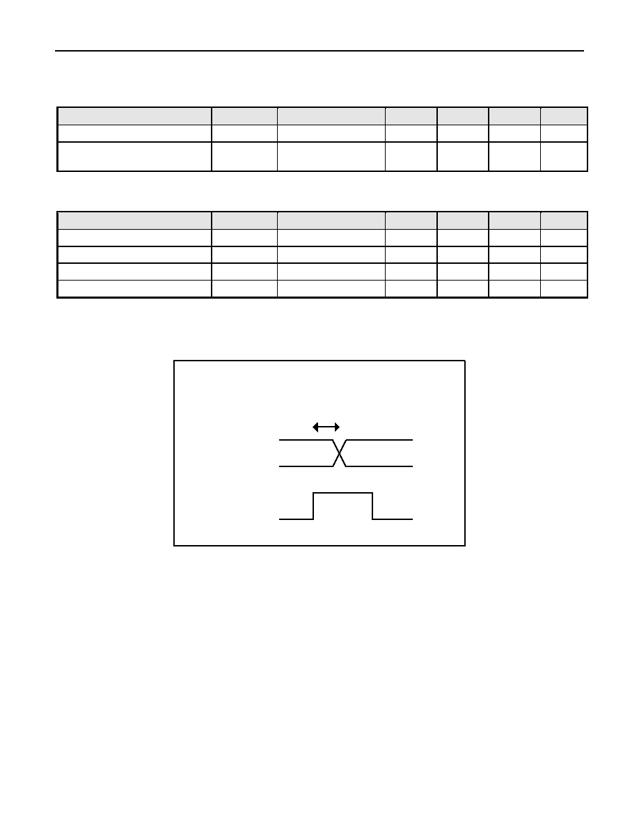
SERIAL-PORT TIMING CHARACTERISTICS:
PARAMETER
SYMBOL
CONDITIONS
MIN
TYP
MAX
UNIT
SDI to SCK setup time
tsu
2
ns
SDI to SCK hold time
th
2
ns
SCK to SDO propagation
delay
tprop
3 ns
1
SA0
SA1
SA2
PA0
PA1
PA2
PA3
Z
CS
SCK
SDI
SDO
t
su
t
h
X
X or Z
t
su
t
h
D0
D1
D2
D3
D4
D5
D6
D7
Z
t
prop
Figure 9: Read Operation
Figure 10: Write Operation
0
SA0
SA1
SA2
PA0
PA1
PA2
PA3
D0
D1
D2
D3
D4
D5
D6
D7
Z
CS
SCK
SDI
SDO
t
su
t
h
X
X
t
su
t
h
78P2351 Single Channel OC-3/STM1-E/E4 Line Interface Unit
21
ELECTRICAL SPECIFICATIONS
(continued)
TRANSMITTER TIMING CHARACTERISTICS:
PARAMETER
SYMBOL
CONDITIONS
MIN
NOM
MAX
UNIT
Clock Duty Cycle
TTCF/TTC
50
%
Transition Time
TTCT
10%-90%
1
ns
Setup Time
TPS
Parallel mode
4
ns
Hold Time
TPH
Parallel mode
4
ns
Setup Time
TSS
Serial mode
1
ns
Hold Time
TSH
Serial mode
1
ns
TIMING DIAGRAM: Transmitter Waveforms
SIDP/N
TSS
TSH
PIxD
TPS
TPH
78P2351 Single Channel OC-3/STM1-E/E4 Line Interface Unit
22
ELECTRICAL SPECIFICATIONS
(continued)
REFERENCE CLOCK CHARACTERISTICS:
PARAMETER
SYMBOL
CONDITIONS
MIN
NOM
MAX
UNIT
CKREF Duty Cycle
--
40
60
%
CKREF Frequency Stability
--
w.r.t. line-rate
frequency
-20 +20
ppm
RECEIVER TIMING CHARACTERISTICS:
PARAMETER
SYMBOL
CONDITIONS
MIN
NOM
MAX
UNIT
Transition Time
TRCT
1
ns
Receive Clock Duty Cycle
TRCF/TRC
50
%
Clock to Q
RSCQ
Serial mode
0.6
ns
Clock to Q
RPCQ
Parallel mode
0.6
ns
TIMING DIAGRAM: Receive Waveforms
Data
Clock
RSCQ
RPCQ

78P2351 Single Channel OC-3/STM1-E/E4 Line Interface Unit
23
ELECTRICAL SPECIFICATIONS
(continued)
TRANSMITTER SPECIFICATIONS FOR CMI INTERFACE
Bit Rate: 139.264Mbit/s
±
15ppm or 155.52Mbits/s
±
20ppm
Code: coded mark inversion (CMI)
Relevant Specification: ITU-T G.703
With the coaxial output port driving a 75
load, the output pulses conform to the templates in Figures 11, 12, 13
and 14. These specifications are tested during production test.
PARAMETER
CONDITION
MIN
NOM
MAX
UNIT
Peak-to-peak Output Voltage
Template, steady state
0.9
1.1
V
Rise/ Fall Time
10-90%
2
ns
Transition Timing Tolerance
Negative Transitions
Positive Transitions at Interval
Boundaries
Positive Transitions at mid-
interval
-0.1
-0.5
-0.35
0.1
0.5
0.35
ns
ns
ns
The following specifications are not tested during production test. They are included for information only.
Note that the return loss depends on the board layout and the particular transformer used.
PARAMETER
CONDITION
MIN
NOM
MAX
UNIT
Return Loss
7MHz to 240MHz
15
dB

78P2351 Single Channel OC-3/STM1-E/E4 Line Interface Unit
24
ELECTRICAL SPECIFICATIONS
(continued)
(Note 1)
(Note 1)
(Note 1)
0.60
0.55
0.50
0.45
0.40
0.05
-0.05
-0.50
-0.55
-0.60
-0.45
-0.40
(Note 1)
0.35ns
Nominal
Zero Level
(Note 2)
T = 7.18ns
0.1ns
0.1ns
1ns
1.795 ns
1.795 ns
1.795 ns
1.795 ns
1ns
1ns
1ns
0.1ns
0.1ns
1ns
1ns
Nominal
Pulse
0.35ns
V
Note 1 ≠ The maximum "steady state" amplitude should not exceed the 0.55V limit. Overshoots and other transients are permitted to fall into
the shaded area bounded by the amplitude levels 0.55V and 0.6V, provided that they do not exceed the steady state level by more than
0.05V.
Note 2 ≠ For all measurements using these masks, the signal should be AC coupled, using a capacitor of not less than 0.01
µ
F, to the input of
the oscilloscope used for measurements. The nominal zero level for both masks should be aligned with the oscilloscope trace with no input
signal. With the signal then applied, the vertical position of the trace can be adjusted with the objective of meeting the limits of the masks. Any
such adjustment should be the same for both masks and should not exceed
±
0.05V. This may be checked by removing the input signal again
and verifying that the trace lies with
±
0.05V of the nominal zero level of the masks.
Note 3 ≠ Each pulse in a coded pulse sequence should meet the limits of the relevant mask, irrespective of the state of the preceding or
succeeding pulses, with both pulse masks fixed in the same relation to a common timing reference, i.e. with their nominal start and finish
edges coincident. The masks allow for HF jitter caused by intersymbol interference in the output stage, but not for jitter present in the timing
signal associated with the source of the interface signal. When using an oscilloscope technique to determine pulse compliance with the mask,
it is important that successive traces of the pulses overlay in order to suppress the effects of low frequency jitter. This can be accomplished by
several techniques [e.g. a) triggering the oscilloscope on the measured waveform or b) providing both the oscilloscope and the pulse output
circuits with the same clock signal].
Note 4 ≠ For the purpose of these masks, the rise time and decay time should be measured between ≠0.4V and 0.4V, and should not exceed
2ns.
Figure 11 ≠ Mask of a Pulse corresponding to a binary Zero in E4 mode
78P2351 Single Channel OC-3/STM1-E/E4 Line Interface Unit
25
ELECTRICAL SPECIFICATIONS
(continued)
(Note 1)
(Note 1)
0.60
0.55
0.50
0.45
0.40
0.05
-0.05
-0.50
-0.55
-0.60
-0.45
-0.40
(Note 1)
Nominal
Zero Level
(Note 2)
T = 7.18ns
0.1ns
0.1ns
1ns
1.795 ns
1ns
Nominal
Pulse
V
3.59ns
1.35ns
1.35ns
3.59ns
1.795 ns
1ns
1ns
0.5ns
0.5ns
Note 1 ≠ The maximum "steady state" amplitude should not exceed the 0.55V limit. Overshoots and other transients are permitted to fall into
the shaded area bounded by the amplitude levels 0.55V and 0.6V, provided that they do not exceed the steady state level by more than
0.05V.
Note 2 ≠ For all measurements using these masks, the signal should be AC coupled, using a capacitor of not less than 0.01
µ
F, to the input of
the oscilloscope used for measurements. The nominal zero level for both masks should be aligned with the oscilloscope trace with no input
signal. With the signal then applied, the vertical position of the trace can be adjusted with the objective of meeting the limits of the masks. Any
such adjustment should be the same for both masks and should not exceed
±
0.05V. This may be checked by removing the input signal again
and verifying that the trace lies with
±
0.05V of the nominal zero level of the masks.
Note 3 ≠ Each pulse in a coded pulse sequence should meet the limits of the relevant mask, irrespective of the state of the preceding or
succeeding pulses, with both pulse masks fixed in the same relation to a common timing reference, i.e. with their nominal start and finish
edges coincident. The masks allow for HF jitter caused by intersymbol interference in the output stage, but not for jitter present in the timing
signal associated with the source of the interface signal. When using an oscilloscope technique to determine pulse compliance with the mask,
it is important that successive traces of the pulses overlay in order to suppress the effects of low frequency jitter. This can be accomplished by
several techniques [e.g. a) triggering the oscilloscope on the measured waveform or b) providing both the oscilloscope and the pulse output
circuits with the same clock signal].
Note 4 ≠ For the purpose of these masks, the rise time and decay time should be measured between ≠0.4V and 0.4V, and should not exceed
2ns.
Note 5 ≠The inverse pulse will have the same characteristics, noting that the timing tolerance at the level of the negative and positive
transitions are
±
0.1ns and
±
0.5ns respectively.
Figure 12 ≠ Mask of a Pulse corresponding to a binary One in E4 mode.

78P2351 Single Channel OC-3/STM1-E/E4 Line Interface Unit
26
ELECTRICAL SPECIFICATIONS
(continued)
(Note 1)
(Note 1)
(Note 1)
0.60
0.55
0.50
0.45
0.40
0.05
-0.05
-0.50
-0.55
-0.60
-0.45
-0.40
(Note 1)
0.35ns
Nominal
Zero Level
(Note 2)
T = 6.43ns
0.1ns
0.1ns
1ns
1.608ns
1.608ns
1.608ns
1.608ns
1ns
1ns
1ns
0.1ns
0.1ns
1ns
1ns
Nominal
Pulse
0.35ns
V
Note 1 ≠ The maximum "steady state" amplitude should not exceed the 0.55V limit. Overshoots and other transients are permitted to fall into
the shaded area bounded by the amplitude levels 0.55V and 0.6V, provided that they do not exceed the steady state level by more than
0.05V.
Note 2 ≠ For all measurements using these masks, the signal should be AC coupled, using a capacitor of not less than 0.01
µ
F, to the input of
the oscilloscope used for measurements. The nominal zero level for both masks should be aligned with the oscilloscope trace with no input
signal. With the signal then applied, the vertical position of the trace can be adjusted with the objective of meeting the limits of the masks. Any
such adjustment should be the same for both masks and should not exceed
±
0.05V. This may be checked by removing the input signal again
and verifying that the trace lies with
±
0.05V of the nominal zero level of the masks.
Note 3 ≠ Each pulse in a coded pulse sequence should meet the limits of the relevant mask, irrespective of the state of the preceding or
succeeding pulses, with both pulse masks fixed in the same relation to a common timing reference, i.e. with their nominal start and finish
edges coincident. The masks allow for HF jitter caused by intersymbol interference in the output stage, but not for jitter present in the timing
signal associated with the source of the interface signal. When using an oscilloscope technique to determine pulse compliance with the mask,
it is important that successive traces of the pulses overlay in order to suppress the effects of low frequency jitter. This can be accomplished by
several techniques [e.g. a) triggering the oscilloscope on the measured waveform or b) providing both the oscilloscope and the pulse output
circuits with the same clock signal].
Note 4 ≠ For the purpose of these masks, the rise time and decay time should be measured between ≠0.4V and 0.4V, and should not exceed
2ns.
Figure 13 ≠ Mask of a Pulse corresponding to a binary Zero in STM-1/STS-3 mode.

78P2351 Single Channel OC-3/STM1-E/E4 Line Interface Unit
27
ELECTRICAL SPECIFICATIONS
(continued)
(Note 1)
(Note 1)
0.60
0.55
0.50
0.45
0.40
0.05
-0.05
-0.50
-0.55
-0.60
-0.45
-0.40
(Note 1)
Nominal
Zero Level
(Note 2)
6.43ns
0.1ns
0.1ns
1ns
1.608ns
1ns
Nominal
Pulse
V
3.215ns
1.2ns
1.2ns
3.215ns
1.608ns
1ns
1ns
0.5ns
0.5ns
Note 1 ≠ The maximum "steady state" amplitude should not exceed the 0.55V limit. Overshoots and other transients are permitted to fall into
the shaded area bounded by the amplitude levels 0.55V and 0.6V, provided that they do not exceed the steady state level by more than
0.05V.
Note 2 ≠ For all measurements using these masks, the signal should be AC coupled, using a capacitor of not less than 0.01
µ
F, to the input of
the oscilloscope used for measurements. The nominal zero level for both masks should be aligned with the oscilloscope trace with no input
signal. With the signal then applied, the vertical position of the trace can be adjusted with the objective of meeting the limits of the masks. Any
such adjustment should be the same for both masks and should not exceed
±
0.05V. This may be checked by removing the input signal again
and verifying that the trace lies with
±
0.05V of the nominal zero level of the masks.
Note 3 ≠ Each pulse in a coded pulse sequence should meet the limits of the relevant mask, irrespective of the state of the preceding or
succeeding pulses, with both pulse masks fixed in the same relation to a common timing reference, i.e. with their nominal start and finish
edges coincident. The masks allow for HF jitter caused by intersymbol interference in the output stage, but not for jitter present in the timing
signal associated with the source of the interface signal. When using an oscilloscope technique to determine pulse compliance with the mask,
it is important that successive traces of the pulses overlay in order to suppress the effects of low frequency jitter. This can be accomplished by
several techniques [e.g. a) triggering the oscilloscope on the measured waveform or b) providing both the oscilloscope and the pulse output
circuits with the same clock signal].
Note 4 ≠ For the purpose of these masks, the rise time and decay time should be measured between ≠0.4V and 0.4V, and should not exceed
2ns.
Note 5 ≠The inverse pulse will have the same characteristics, noting that the timing tolerance at the level of the negative and positive
transitions are
±
0.1ns and
±
0.5ns respectively.
Figure 14 ≠ Mask of a Pulse corresponding to a binary One in STM-1/STS-3 mode

78P2351 Single Channel OC-3/STM1-E/E4 Line Interface Unit
28
ELECTRICAL SPECIFICATIONS
(continued)
TRANSMITTER OUTPUT JITTER
The transmit jitter specification ensures compliance with ITU-T G.813, G.823, G.825 and G.958; ANSI T1.102-
1993 and T1.105.03-1994; and GR-253-CORE for all supported rates. Transmit output jitter is not tested during
production test.
PARAMETER
CONDITION
MIN
NOM
MAX
UNIT
CMI Mode;
200 Hz to 3.5 MHz, measured
with respect to CKREF for 60s
0.075 UIpp
Transmitter Output Jitter
NRZ (optical) Mode;
12 kHz to 1.3 MHz, measured
with respect to CKREF
0.01 UIrms
Transmitter
Output
Jitter
Detector
Measured Jitter
Amplitude
f1
f2
20dB/decade
78P2351 Single Channel OC-3/STM1-E/E4 Line Interface Unit
29
ELECTRICAL SPECIFICATIONS
(continued)
RECEIVER (Transformer-coupled)
PARAMETER
CONDITION
MIN
TYP
MAX
UNIT
Peak Differential Input
Amplitude, RXP and RXN
CMI mode; MON=0.
500 mVpk
Peak Differential Input
Amplitude, RXP and RXN
CMI mode; MON=1
50
mVpk
Flat-loss Tolerance
CMI mode; MON=0.
All valid cable lengths.
2 dB
Receive Clock Jitter
STM-1 mode; CMI mode
with maximum cable
a) Normal receive mode
b) Remote
loopback
mode
0.1
0.07
UIpp
UIpp
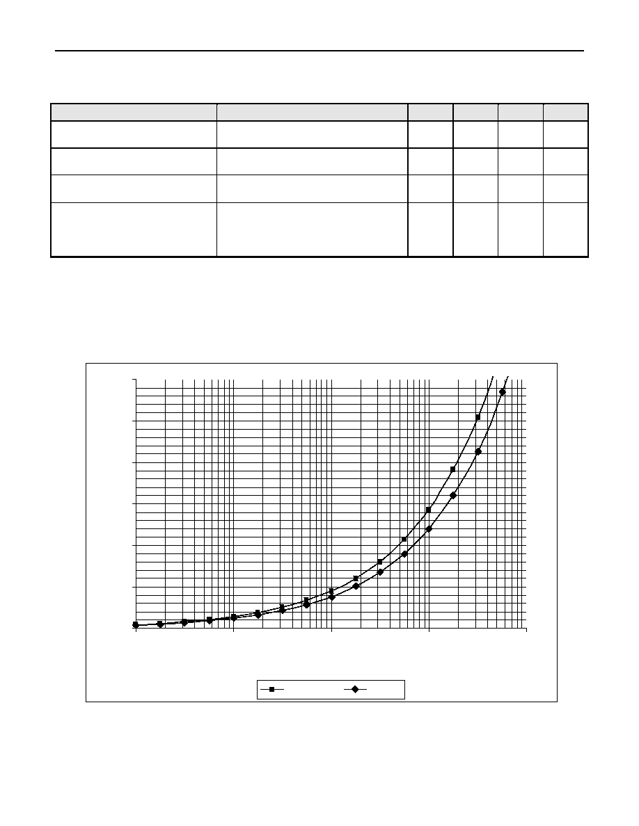
RECEIVER SPECIFICATIONS FOR CMI INTERFACE
The input signal is assumed compliant with ITU-T G.703 and can be attenuated by the dispersive loss of a
cable. The minimum cable loss is 0dB and the maximum is ≠12dB at 70MHz.
The "Worst Case" line corresponds to the ITU-T G.703 recommendation. The "Typical" line corresponds to a
typical installation referred to in ANSI T1.102-1993. The receiver is tested using the cable model. It is a lumped
element approximation of the "Worst Case" line.
Figure 15: Typical and worst-case Cable attenuation
0
5
10
15
20
25
30
1.00E+05
1.00E+06
1.00E+07
1.00E+08
1.00E+09
Frequency (Hz)
A
tten
u
a
ti
o
n
(d
B
)
Worst Case
Typical
78P2351 Single Channel OC-3/STM1-E/E4 Line Interface Unit
30
ELECTRICAL SPECIFICATIONS
(continued)
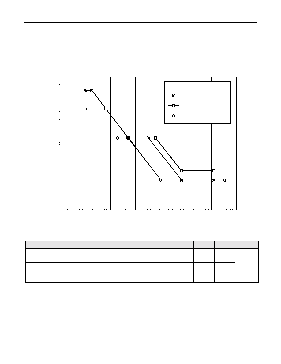
RECEIVER JITTER TOLERANCE
The 78P2351 is compliant with all relevant jitter tolerance specifications shown in Figures 16, 17. STS-3/OC-3
jitter tolerance specifications are in ANSI T1.105.03-1994 and Telcordia GR-253-CORE. STM-1 (optical) jitter
tolerance specifications are in ITU-T G.813, G.825, and G.958. STM-1e (electrical) jitter tolerance
specifications are in ITU-T G.825. E4 specifications are found in ITU-T G.823. Receive jitter tolerance is not
tested during production test.
0.01
0.1
1
10
100
1.E+00
10Hz
100Hz
1kHz
10kHz
100kHz
1MHz
10MHz
Electrical (CMI) Interfaces
G.825 - STM-1e Tolerance
(for 2048 kbps networks)
G.825 - STM-1e Tolerance
(for 1544 kbps networks)
Jitter Frequency
Jit
t
e
r
To
ler
a
nc
e (
U
I
pp
)
G.823 - E4 Tolerance
Figure 16: Jitter Tolerance - electrical (CMI) interfaces
PARAMETER
CONDITION
MIN
NOM
MAX
UNIT
E4 Jitter Tolerance
200Hz to 500Hz
10kHz to 3.5MHz
1.5
0.075
STM-1e Jitter Tolerance
10Hz to 19.3Hz
68.7Hz to 6.5kHz
65kHz to 1.3MHz
38.9
1.5
0.15
UIpp
78P2351 Single Channel OC-3/STM1-E/E4 Line Interface Unit
31
ELECTRICAL SPECIFICATIONS
(continued)
0.01
0.1
1
10
100
1.E+00
10Hz
100Hz
1kHz
10kHz
100kHz
1MHz
10MHz
Optical (NRZ) Interfaces
G.813, G.958, T1.105.03, GR-253
STM-1 / STS-3 / OC-3 Tolerance
G.825 - STM-1 Tolerance
Jitter Frequency
Jit
t
e
r
To
ler
a
nc
e (
U
I
pp
)
Figure 17: Jitter Tolerance - optical (NRZ) interfaces
PARAMETER
CONDITION
MIN
NOM
MAX
UNIT
OC-3/STS-3/STM-1 (optical)
Jitter Tolerance
10Hz to 19.3Hz
68.7Hz to 6.5kHz
65kHz to 1.3MHz
38.9
1.5
0.15
UIpp

78P2351 Single Channel OC-3/STM1-E/E4 Line Interface Unit
32
ELECTRICAL SPECIFICATIONS
(continued)
RECEIVER JITTER TRANSFER FUNCTION
The receiver clock recovery loop filter characteristics such that the receiver has the following transfer function.
The corner frequency of the PLL is approximately 120 kHz. Receiver jitter transfer function is not tested during
production test.
-10
-9
-8
-7
-6
-5
-4
-3
-2
-1
0
1.00E+03
1.00E+04
1.00E+05
1.00E+06
1.00E+07
Figure 18: Jitter Transfer
PARAMETER
CONDITION
MIN
NOM
MAX
UNIT
Receiver Jitter transfer function
below 120 kHz
0.1
dB
Jitter transfer function roll-off
20
dB per
decade
78P2351 Single Channel OC-3/STM1-E/E4 Line Interface Unit
33
ELECTRICAL SPECIFICATIONS
(continued)
CMI Mode Loss of Signal Condition
T1517720-95/d01
P
Q
N
o
m
i
n
a
l
v
a
l
u
e
M
a
ximum
c
a
b
le loss
3
d
B
"Transition condition" must be detected
T
o
lerance range
"
N
o
t
r
a
n
s
i
t
i
o
n
c
o
n
d
i
t
i
o
n
"
o
r
"transition condition" may be detected
"No transition condition" must be detecte
d
N
O
T
E
S
1
T
h
e
s
i
g
n
a
l
l
e
v
e
l
P
i
s
(
m
a
x
i
m
u
m
c
a
b
l
e loss +3) dB below nominal.
2
T
h
e
s
i
g
n
a
l
l
e
v
e
l
Q
i
s
g
r
e
a
t
e
r
t
h
a
n
t
h
e
maximum expected cross-talk level.
L
e
v
e
l
b
e
l
o
w
N
o
m
i
n
a
l

78P2351 Single Channel OC-3/STM1-E/E4 Line Interface Unit
34
APPLICATION INFORMATION
EXTERNAL COMPONENTS:
COMPONENT
PIN(S)
VALUE
UNITS
TOLERANCE
Receiver Termination Resistor
RXP
RXN
75
1%
Transmitter Termination Resistor
CMIP
CMIN
75
1%
TRANSFORMER SPECIFICATIONS:
COMPONENT
VALUE
UNITS
TOLERANCE
Turns Ratio for the Receiver
1:1
Turns Ratio for the Transmitter (center-tapped)
1:1
Suggested Manufacturer: Pulse, MiniCircuits
RECOMMENDED LVPECL TERMINATIONS:
= 50
= 50
= 50
= 50
= 50
= 50
= 50
= 50
100
100
100
100
200
200
200
200
200
200
200
200
O/E converter
or
OC3 Framer
RXP/N
or
SIDP/N
Figure 19: Differential LVPECL Inputs
E/O Converter
= 50
= 50
= 50
= 50
= 50
= 50
= 50
= 50
100
100
100
100
200
200
200
200
200
200
200
200
ECLP/N
Figure 20: Differential LVPECL Outputs

78P2351 Single Channel OC-3/STM1-E/E4 Line Interface Unit
35
MECHANICAL SPECIFICATIONS
15.7 (0.618)
16.3 (0.641)
PIN No. 1
Indicator
+
15.7 (0.618)
16.3 (0.641)
13.8 (0.543) SQ
14.2 (0.559)
1.40 (0.055)
1.60 (0.063)
0.00(0)
0.20 (0.008)
0.60 (0.024) TYP.
0.50 TYP.
(0.0197)
0.18( 0.007)
0.27 (0.011)
100-pin TQFP (JEDEC LQFP)

78P2351 Single Channel OC-3/STM1-E/E4 Line Interface Unit
36
PACKAGE INFORMATION
(Top View)
1
2
3
4
5
6
7
8
9
10
11
12
13
14
15
16
17
18
19
20
21
22
23
24
25
26
27
28
29
30
31
32
33
34
35
36
37
38
39
40
41
42
43
44
45
46
47
48
49
50
63
62
61
60
59
58
57
56
55
54
53
52
51
64
65
66
67
68
69
70
71
72
73
74
75
76
77
78
79
80
81
82
83
84
85
86
87
88
89
90
91
92
93
94
95
96
97
98
99
100
N/
C
ECL
N
ECLP
VCC
TXCKN
TXCKP
GN
D
CMI
N
CMI
P
VCC
RXN
RXP
GN
D
VCC
GN
D
GN
D
GN
D
GN
D
CKR
E
FP
VCC
CMI
2
P
CMI
2
N
GN
D
VCC
CKR
E
FN
PO1D
N/
C
N/
C
N/
C
N/
C
N/
C
N/
C
N/
C
VD
D
VS
S
PO0D
VD
D
PO2D
VS
S
PO3D
VD
D
VS
S
PO
C
K
VD
D
VS
S
N/
C
PT
O
C
K
PI
3D
N/
C
PI
2D
TXOUT1
TXOUT0
VCC
GND
VCC
SIDN
SODN
PICK
PI0D
PI1D
SICKP
SICKN
N/C
SIDP
N/C
VCC
GND
TXPD
CKMODE
SOCKP
GND
SOCKN
SODP
LPBK
RCSL
GND
POR
CKSL
LOS
GND
SDI_PAR
SDO_E4
N/C
N/C
SCK_MON
SEN_CMI
LOL
FRST
SPSL
INTTX
VCC
GND
GND
N/C
N/C
INTRX
N/C
VCC
VCC
N/C
78P2351-IGT
Target Datasheet:
This Target Datasheet is proprietary to TDK Semiconductor Corporation (TSC) and sets forth design goals for the
described product. The data sheet is subject to change. TSC assumes no obligation regarding future manufacture, unless agreed to in
writing.
If and when manufactured and sold, this product is sold subject to the terms and conditions of sale supplied at the time of order
acknowledgment, including those pertaining to warranty, patent infringement and limitation of liability. TDK Semiconductor Corporation
(TSC) reserves the right to make changes in specifications at any time without notice. Accordingly, the reader is cautioned to verify that a
data sheet is current before placing orders. TSC assumes no liability for applications assistance.
TDK Semiconductor Corp., 2642 Michelle Dr., Tustin, CA 92780
TEL (714) 508-8800, FAX (714) 508-8877, http://www.tdksemiconductor.com
©
2003 TDK Semiconductor Corporation
04/03/03 ≠ rev 1.5

78P2351 Single Channel OC-3/STM1-E/E4 Line Interface Unit
37
Revison History
v1-3
February 13, 2003
: Initial customer release
v1-4
March 25, 2003
: Modified pinout (pins 67-69) ; Added conditions for LCV ; Added thermal data ;
Updated Jitter Specs ;
V1-5
April 3, 2003
: corrected Pin Description for CMI2P/N