 | –≠–ª–µ–∫—Ç—Ä–æ–Ω–Ω—ã–π –∫–æ–º–ø–æ–Ω–µ–Ω—Ç: TC18C46-1 | –°–∫–∞—á–∞—Ç—å:  PDF PDF  ZIP ZIP |
Document Outline
- Return to Contents
- List of Figures
- 1. R1 and R2 Set Maximum Peak Output Current
- 2. Resistive Sensing
- 3. Transformer Isolated Current Sense
- 4. Master/Slave Parallel Operation
- 5. External Clock Synchronization
- 6. Oscillator Circuit
- Features
- Functional Block Diagram
- General Description
- Ordering Information
- Absolute Maximum Ratings
- Pin Configurations
- Electrical Characteristics: unless otherwise stated, these specifications apply for TA = Ö 55∞C to
- Peak Current Limit Setup
- Output Shutdown
- Soft Restart From Shutdown
- Soft-Start Power-Up
- Current-Sense Amplifier
- Under Voltage Lockout
- Circuit Synchronization
- Selection of Timing Capacitor and Resistor
- Typical Characteristics
- Pin Description
4-101
TELCOM SEMICONDUCTOR, INC.
7
6
5
4
3
1
2
8
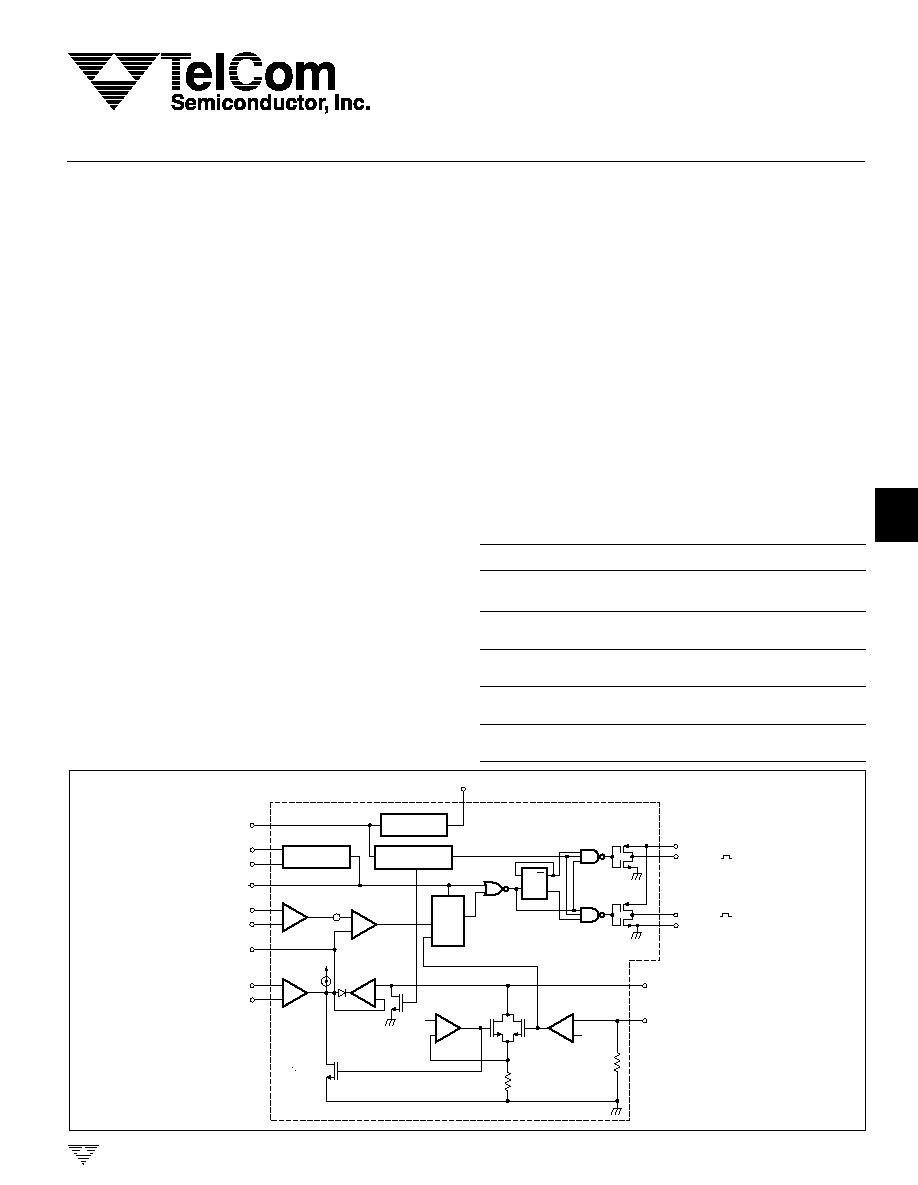
FUNCTIONAL BLOCK DIAGRAM
GENERAL DESCRIPTION
The TC38C46 is a current mode CMOS PWM control
IC. It draws only 2 mA supply current, so it can be driven
without a costly 50-60 Hz transformer. The output drive
stage is capable of high drive currents, 300mA typical.
The TC38C46 is pin compatible with earlier bipolar
products so that designers can easily update older designs.
A number of improvements have been added.
This second generation part has been designed with an
isolated drive stage. Unlike its cousin, the TC170, the output
stage of the TC38C46 can be run from a separate power
supply such as a secondary winding on an output trans-
former. This allows for bootstrap start-up of the power
supply.
CMOS CURRENT MODE PWM CONTROLLER
FEATURES
s
Isolated Output Drive
s
Low Power CMOS Construction
s
Low Supply Current ................................. 2mA Typ.
s
Wide Supply Voltage Operation .............. 8V to 18V
s
Latch-Up Immunity ................... 500mA on Outputs
s
Above and Below Rail Input Protection ............. 6V
s
High Output Drive ................................ 500mA Peak
s
Current Mode Control
s
Fast Rise/Fall Time ..................... 50nsec @ 1000pF
s
High Frequency Operation .......................... 500kHz
s
UV Hysteresis Guaranteed
s
Programmable Current Limit
s
Shutdown Pin Available
s
Double Ended
s
Soft Start
s
Low Prop Delay Current Amp
to Output ......................................... < 350nsec Typ.
s
Low Prop Delay Shutdown
to Output ......................................... < 400nsec Typ.
s
TC38C46Pin Compatible with Unitrode UC3846
s
ESD Protected .................................................
±
2 kV
+
≠
+
≠
+VS
+
+
≠
.65V
≠ +
+
≠
D
Q
C
Q
100
µ
A
PWM
COMPARATOR
LIMIT BUFFER
AMPLIFIER
LOCK-UP
AMPLIFIER
CURRENT SENSE
AMPLIFIER
ERROR
AMPLIFIER
350mV
Q1
Q2
3.5k
350mV
6k
SHUTDOWN
COMPARATOR
SHUTDOWN
CURRENT LIMIT
SOFT START ADJUST
TC38C46 OUTPUTS
LOW IN OFF STATE
OUTPUT A
VDD
GROUND
OUTPUT B
PWM LATCH
VIN
RT
CT
SYNC
≠ CURRENT
SENSE INPUT
+ ERROR
AMP INPUT
≠ ERROR
AMP INPUT
+ CURRENT
SENSE INPUT
COMPENSATION
Q3
VREF
2
12
14
1
16
11
13
15
9
8
10
3
4
7
5
6
TC18C46
TC28C46
TC38C46
Q4
POSITIVE
FEEDBACK
+
≠
+
≠
5.1 VOLT
REFERENCE
UNDER VOLTAGE
LOCKOUT
OSCILLATOR
S
Q
S
R
x3
ORDERING INFORMATION
Part No.
Configuration
Pkg./Temperature
TC18C46MJE
Non-Inverting
16-Pin CerDIP
≠ 55
∞
C to +125
∞
C
TC28C46EOE
Non-Inverting
16-Pin SOIC (Wide)
≠ 40
∞
C to +85
∞
C
TC28C46EPE
Non-Inverting 16-Pin Plastic DIP (Narrow)
≠ 40
∞
C to +85
∞
C
TC38C46COE
Non-Inverting
16-Pin SOIC (Wide)
0
∞
C to +70
∞
C
TC38C46CPE
Non-Inverting
16-Pin Plastic DIP (Narrow)
0
∞
C to +70
∞
C
TC18/28/28/C46-8 9/23/96
TC18C46
TC28C46
TC38C46

4-102
TELCOM SEMICONDUCTOR, INC.
ABSOLUTE MAXIMUM RATINGS
Output Current, Source or Sink (Pins 1, 14) .......... 500mA
Analog Inputs (Pins 3, 4, 5, 6, 16) .............. ≠ 0.3V to +V
IN
Reference Output Current (Pin 2) ........................ ≠ 30 mA
Sync Output Current (Pin 10) .................................. ≠ 5mA
Error Amplifier Output Current (Pin 7) ..................... ≠ 5mA
Soft Start Sink Current (Pin 1) .................................. 50mA
Oscillator Charging Current (Pin 9) ............................ 5mA
Supply Voltage ............................................................ 18V
Maximum Chip Temperature ................................... 150
∞
C
Storage Temperature ............................ ≠ 65
∞
C to +150
∞
C
Lead Temperature (Soldering, 10 sec) ................... 300
∞
C
Package Thermal Resistance
CerDIP R
J-A .................................................................
150
∞
C/W
CerDIP R
J-C ...................................................................
55
∞
C/W
PDIP R
J-A .....................................................................
125
∞
C/W
PDIP R
J-C ........................................................................
45
∞
C/W
SOIC R
J-A .....................................................................
250
∞
C/W
SOIC R
J-C .......................................................................
75
∞
C/W
NOTES:
1. All voltages are with respect to Ground, Pin 12. Currents are positive into,
negative out of the specified terminal.
2. Static-sensitive device. Unused devices must be stored in conductive
material. Protect devices from static discharge and static fields. Stresses
above those listed under Absolute Maximum Ratings may cause perma-
nent damage to the device. These are stress ratings only and functional
operation of the device at these or any other conditions above those
indicated in the operational sections of the specifications is not implied.
Exposure to Absolute Maximum Rating Conditions for extended periods
may affect device reliability.
PIN CONFIGURATIONS
8
1
14
2
13
3
12
4
11
5
10
6
9
7
VDD
+ CURRENT SENSE
15
16
OUTPUT B
≠ CURRENT SENSE
VIN
VREF
SHDN
CURRENT LIMIT/
SOFT START
GND
+ ERROR AMP
OUTPUT A
≠ ERROR AMP
SYNC
COMP
RT
CT
TC18C46MJE
TC28C46EPE
TC38C46CPE
8
1
14
2
13
3
12
4
11
5
10
6
9
7
15
16
TC28C46EOE
TC38C46COE
VDD
+ CURRENT SENSE
OUTPUT B
≠ CURRENT SENSE
VIN
VREF
SHDN
CURRENT LIMIT/
SOFT START
GND
+ ERROR AMP
OUTPUT A
≠ ERROR AMP
SYNC
COMP
RT
CT
16-Pin Plastic DIP (Narrow)
16-Pin CerDIP
16-Pin SOIC (Wide)
CMOS CURRENT MODE
PWM CONTROLLERS
TC18C46
TC28C46
TC38C46

4-103
TELCOM SEMICONDUCTOR, INC.
7
6
5
4
3
1
2
8
ELECTRICAL CHARACTERISTICS:
unless otherwise stated, these specifications apply for T
A
= ≠ 55
∞
C to
+125
∞
C for TC18C46; ≠ 40
∞
C to +85
∞
C for the TC28C46; and 0
∞
C to +70
∞
C for the TC38C46; V
IN
= V
DD
= 16V;
R
T
= 30.1k; C
T
= 270pF.
TC18C46
TC28C46
TC38C46
Parameter
Test Conditions
Min
Typ
Max
Min
Typ
Max
Units
Reference Section
Output Voltage
T
f
= 25
∞
C, I
O
= 1mA
5.0
5.1
5.2
5.0
5.1
5.2
V
Line Regulation
V
IN
= 8V to 16V
--
4
20
--
4
20
mV
Load Regulation
I
O
= 1mA to 10mA
--
4
20
--
4
20
mV
Temp Coefficient
Over Operating Range, (Note 1)
--
0.2
0.5
--
0.2
0.5
mV/
∞
C
Total Output Range
Line, Load, and Temperature (Note 1)
4.97
--
5.24
4.94
--
5.26
V
Long Term Drift
T
f
= 125
∞
C, 1000 Hrs (Note 1)
--
50
--
--
50
--
mV
Short Circuit
V
REF
= 0V
20
--
70
20
--
70
mA
Output Current
Output Noise Voltage
10 Hz
f
10 kHz, Tf
= 25
∞
C (Note 1)
--
22
--
--
22
--
µ
V(rms)
Oscillator Section
Initial Accuracy
T
f
= 25
∞
C
96.5
102
106.5
96.5
101
106.5
kHz
Voltage Coefficient
V
IN
= 8V to 16V
--
.1
2.0
--
.1
1.5
%/V
Temp Coefficient
Over Operating Range (Note 1)
--
.04
0.06
--
.04
0.06
%/
∞
C
Clock Ramp
1.2
2
3
1.2
2
3
mA
Reset Current
Osc Ramp Amplitude
3.6
3.8
4
3.6
3.8
4
V
Sync Output High Level
(Note 1)
V
DD
--
--
V
DD
--
--
V
≠0.5
≠0.5
Sync Output Low Level
(Note 1)
--
--
0.5
--
--
0.5
V
Sync Input High Level
Pin 8 = 0V, (Note 1)
--
8.5
--
--
8.5
--
V
Sync Input Low Level
Pin 8 = 0V, (Note 1)
--
8.5
5
--
8.5
5
V
Sync Input Current
Sync Voltage = 5.25V, Pin 8 = 0V
--
±
5
50
--
±
5
50
nA
Error Amp Section
Input Offset Voltage
--
±
5
±
25
--
±
5
±
25
mV
Input Bias Current
--
±
10
±
100
--
±
0.1
±
0.5
nA
Input Offset Current
--
±
10
±
100
--
±
0.1
±
0.5
nA
Open Loop Voltage Gain
V
O
= 1V to 6V, R
L
= 100k
70
90
--
70
90
--
dB
Gain Bandwidth Product
T
f
= 25
∞
C (Note 1)
0.7
1
--
0.7
1
--
MHz
CMRR
V
CM
= 0V to 11V
70
90
--
70
90
--
dB
PSRR
V
IN
= 8V to 16V
70
90
--
70
90
--
dB
Output Sink Current
V(EA ≠) = 5V, V(EA+) = 4.9V,
2
4
--
2
4
--
mA
V(CMPTR) = 1.2V
Output Source Current
V(EA ≠) = 5V, V(EA+) = 5.1V,
5
10
--
5
10
--
mA
V(CMPTR)
= 2.5V
High Level Output Volt
R
L
= (CMPTR) 5k
to GND, A
CL
= 300
4.75
4.9
5.1
4.75
4.9
5.1
V
Low Level Output Volt
R
L
= (CMPTR) 5k
to GND, A
CL
= 300
--
0.4
0.9
--
0.4
0.9
V
Slew Rate
1.3
2
--
1.3
2
--
V/
µ
sec
CMOS CURRENT MODE
PWM CONTROLLERS
TC18C46
TC28C46
TC38C46

4-104
TELCOM SEMICONDUCTOR, INC.
Current Sense Section
Amplifier Gain
(Notes 2, 3)
2.7
3
3.6
2.7
3
3.4
V/V
Max Differential
(Note 2)
1.1
1.5
1.8
1.1
1.5
1.8
V
Input Signal (V
Pin 4
-V
Pin 3
)
Input Offset Voltage
(Note 2)
0.4
0.65
0.85
0.4
0.65
0.85
V
CMRR
V
CM
= 1V to 12V, (Note 2)
40
60
--
40
60
--
dB
PSRR
V
IN
= 8V to 16V, (Note 2)
40
60
--
40
60
--
dB
Input Bias Current
(Note 1)
--
±
1
±
100
--
±
1
±
100
nA
Input Offset Current
(Note 1)
--
±
0.1
±
2
--
±
0.1
±
2
nA
Input Common Mode Range
(Note 1)
0
--
11
0
--
11
V
Delay to Outputs
T
f
= 25
∞
C, (Note 1)
150
225
400
150
225
400
nsec
Current Limit Adjust Section
Current Limit Voltage Offset
--
±
1
±
25
--
±
1
±
25
mV
Input Impedance
(Shutdown Unlatched)
3
3.5
4
3
3.5
4
k
Shutdown Terminal Section
Threshold Voltage
320
360
400
320
360
400
mV
Input Voltage Range
(Note 1)
0
--
V
IN
0
--
V
IN
V
Min Latching
(Note 4)
140
--
--
140
--
--
µ
A
Current (I
Pin 1
)
Max Non-Latching
(Note 5)
--
--
60
--
--
65
µ
A
Current (I
Pin1
)
Min Pulse Width
(Note 1)
100
50
--
100
50
--
nsec
Delay to Outputs
(Note 1)
125
250
400
125
250
400
nsec
Output Section
Output Low Level r
DS (ON)
I
SINK
= 20mA
--
10
20
--
10
20
Output High Level r
DS (ON)
I
SOURCE
= 20mA
--
20
35
--
20
35
Output Rise Time
C
L
= 1
µ
F
--
55
90
--
55
90
nsec
Output Fall Time
C
L
= 1
µ
F
--
55
90
--
55
90
nsec
Undervoltage Lockout Section
Undervoltage Threshold
6.5
7
7.3
6.5
7
7.3
V
Start Threshold
7.4
7.8
8
7.4
7.8
8
V
Threshold Hysteresis
0.6
0.8
1
0.6
0.8
1
V
Total Standby Current
Supply Current
--
1.2
2.5
--
1.2
2
mA
Start-Up Current
--
250
350
--
250
350
µ
A
ELECTRICAL CHARACTERISTICS (Cont):
Unless otherwise stated, these specifications apply for
T
A
= ≠55
∞
C to +125
∞
C for TC18C46; ≠ 40
∞
C to +85
∞
C for the TC28C46; and 0
∞
C to +70
∞
C for the TC38C46; V
IN
= V
DD
=
16V; R
T
= 30.1k; C
T
= 270pF.
TC18C46
TC28C46 TC38C46
Parameter
Test Conditions
Min
Typ
Max
Min
Typ
Max
Units
NOTES: 1. These parameters, although guaranteed over the
recommended operating conditions, are not tested in
production.
2. Parameter measured at trip point of latch with V
Pin 6
=
V
REF
, V
Pin 16
= 0V.
3. Amplifier gain is defined as:
4. Current into Pin 1 guaranteed to latch circuit in shutdown
state.
5. Current into Pin 1 guaranteed not to latch circuit in
shutdown state.
CMOS CURRENT MODE
PWM CONTROLLERS
TC18C46
TC28C46
TC38C46
G =
VPin 7
;
VPin 4 = 0V to 1V
VPin 4

4-105
TELCOM SEMICONDUCTOR, INC.
7
6
5
4
3
1
2
8
Peak Current Limit Setup
Resistors R1 and R2 at the CURRENT LIMIT input (pin
1) set the peak current limit (Figure 1). The potential at pin
1 is easily calculated:
V1 = V
REF
R2
R1 + R2
R1 should be selected first. The shutdown circuit fea-
ture is not latched for (V
REF
≠ 0.35)/R1 <65
µ
A and is latched
for currents greater than 140
µ
A.
The error amplifier output voltage is clamped from
going above V1 through the limit buffer amplifier. Peak
current is sensed by RS and amplified by the current
amplifier which has a fixed gain of 3.
I
PCL
, the peak current limit, is the current that causes
the PWM comparator noninverting input to exceed V1, the
potential at the inverting input. Once the comparator trip
point is exceeded, both outputs are disabled.
I
PCL
is easily calculated:
I
PCL
=
V1 ≠ 0.65V
3 (RS)
where:
V1 = V
REF
V
REF
= Internal voltage reference = 5.1V
3 = Gain of current-sense amplifier
0.65V = Current limit offset
Both driver OUTPUTs (pins 11 and 14) are OFF (LOW)
when the peak current limit is exceeded. When the sensed
current goes below I
PCL
, the circuit operates normally.
Output Shutdown
The outputs can be turned OFF quickly through the
SHUTDOWN input (pin 16). A signal greater than 360 mV
at pin 16 forces the shutdown comparator output HIGH.
The PWM latch is held set, disabling the outputs.
Q2 is also turned ON. If V
REF
/R1 is greater than 140
µ
A,
positive feedback through the lock-up amplifier and Q1
keeps the inverting PWM comparator inverting input below
0.65V. Q3 remains ON even after the shutdown input
signal is removed. This is because the lock-up amplifier is
in latched mode driving Q3 ON. This state can be cleared
only through a power-up cycle. Outputs will be disabled
whenever the potential at pin 1 is below 0.65V.
The shutdown terminal gives a fast, direct way to dis-
able the PWM controller output transistors. System protec-
tion and remote shutdown applications are possible.
R2
R1 + R2
The input pulse to pin 16 should be at least 100nsec
wide and have an amplitude of at least 1V in order to get the
minimum propagation delay from input to output. If these
parameters are met, the delay should be less than 400nsec
at 25
∞
C; however, the delay time will increase as the device
temperature rises.
Soft Restart From Shutdown
A soft restart can be programmed if nonlatched shut-
down operation is used.
A capacitor at pin 1 will cause a gradual increase in
potential toward V1. When the voltage at pin 1 reaches
0.75V, the PWM latch set input is removed and the circuit
establishes a regulated output voltage. The soft-start opera-
tion forces the PWM output drivers to initially operate with
minimum duty cycle and low peak currents.
Even if a soft start is not required, it is necessary to
insert a capacitor between pin 1 and ground if the current I
L
is greater than 140
µ
A. This capacitor will prevent "noise
triggering" of the latch, yet minimize the soft-start effect.
Soft-Start Power-Up
During power-up, a capacitor at R1, R2 initiates a soft-
start cycle. As the input voltage (pin 15) exceeds the
under-voltage lockout potential (7V), Q4 is turned OFF,
ending undervoltage lockout. Whenever the PWM com-
parator inverting input is below 0.65V, both outputs are
disabled.
When the undervoltage lockout start threshold is ex-
ceeded, the capacitor begins to charge. The PWM duty
cycle increases until the operating output voltage is reached.
Soft-start operation forces the PWM output drivers to initially
operate with minimum duty cycle and low peak current.
Current-Sense Amplifier
The current-sense amplifier operates at a fixed gain of
3. Maximum differential input voltage (V
PIN4
≠V
PIN3
) is 1.1V.
Common-mode input voltage range is 0V to V
IN
≠ 3V.
Resistive-sensing methods are shown in Figure 2. In
Figure 2(A), a simple RC filter limits transient voltage spikes
at pin 4, caused by external output transistor-collector
capacitance. Transformer coupling (Figure 3) offers isola-
tion and better power efficiency, but cost and complexity
increase.
In order to minimize the propagation delay from the input
to the current amplifier to the output terminals, the current
ramp should be in the order of 1
µ
sec in width (min). Typical
time delay values are in the 225nsec region at 25
∞
C. The
delay time increases with device temperature so that at
50
∞
C, the delay times may be increased by as much as
100nsec.
CMOS CURRENT MODE
PWM CONTROLLERS
TC18C46
TC28C46
TC38C46