 | –≠–ª–µ–∫—Ç—Ä–æ–Ω–Ω—ã–π –∫–æ–º–ø–æ–Ω–µ–Ω—Ç: TC428CPA | –°–∫–∞—á–∞—Ç—å:  PDF PDF  ZIP ZIP |
Document Outline
- Return to Contents
- List of Figures
- 1. Inverting Driver Switching Time Test Circuit
- 2. Noninverting Driver Switching Time Test Circuit
- Features
- Pin Configurations
- Functional Block Diagram
- General Description
- Ordering Information
- Absolute Maximum Ratings*
- Electrical Characteristics: TA = +25∞C with 4.5V £ VDD £ 18V, unless otherwise specified.
- Electrical Characteristics: Over Operating Temperature Range with 4.5V £ VDD £ 18V, unless otherwise specified.
- Supply Bypassing
- Grounding
- Input Stage
- Power Dissipation
- Typical Characteristics
- Voltage Doubler
- Voltage Inverter
4-169
TELCOM SEMICONDUCTOR, INC.
7
6
5
4
3
1
2
8
TC426
TC427
TC428
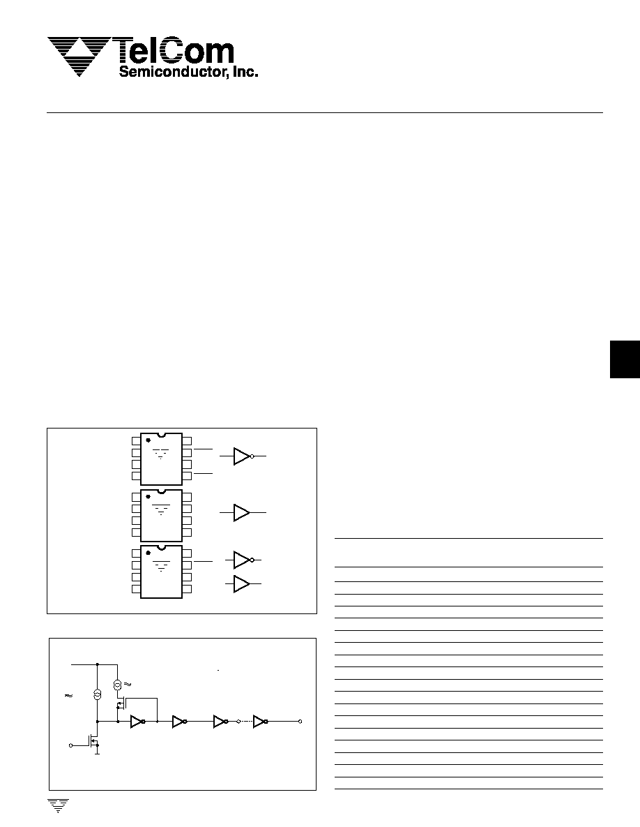
PIN CONFIGURATIONS
(DIP and SOIC)
TC426
1
2
3
4
NC
5
6
7
8
OUT A
OUT B
NC
IN A
GND
IN B
V
DD
NC = NO INTERNAL CONNECTION
2, 4
7, 5
INVERTING
TC427
1
2
3
4
NC
5
6
7
8
OUT A
OUT B
NC
IN A
GND
IN B
2, 4
7, 5
NONINVERTING
TC428
1
2
3
4
NC
5
6
7
8
OUT A
OUT B
NC
IN A
GND
IN B
2
7
4
5
V
DD
V
DD
COMPLEMENTARY
INPUT
V+
2.5mA
500
µ
A
INVERTING
OUTPUT
NONINVERTING
OUTPUT
(TC426)
(TC427)
TC426
TC427
TC428
1.5A DUAL HIGH-SPEED POWER MOSFET DRIVERS
FEATURES
s
High-Speed Switching (C
L
= 1000pF) ........... 30nsec
s
High Peak Output Current ................................. 1.5A
s
High Output Voltage Swing .................. V
DD
≠ 25mV
GND + 25mV
s
Low Input Current (Logic "0" or "1") ................ 1
µ
A
s
TTL/CMOS Input Compatible
s
Available in Inverting and Noninverting
Configurations
s
Wide Operating Supply Voltage ............ 4.5V to 18V
s
Current Consumption
-- Inputs Low .................................................. 0.4mA
-- Inputs High .................................................... 8mA
s
Single Supply Operation
s
Low Output Impedance ........................................ 6
s
Pinout Equivalent of DS0026 and MMH0026
s
Latch-Up Resistant: Withstands > 500mA
Reverse Current
s
ESD Protected ...................................................... 2kV
FUNCTIONAL BLOCK DIAGRAM
Note: The TC428 has one inverting and one noninverting
driver. Ground any unused driver input.
TC426/7/8-7
10/11/96
GENERAL DESCRIPTION
The TC426/TC427/TC428 are dual CMOS high-speed
drivers. A TTL/CMOS input voltage level is translated into
a rail-to-rail output voltage level swing. The CMOS output
is within 25 mV of ground or positive supply.
The low impedance, high-current driver outputs swing
a 1000pF load 18V in 30nsec. The unique current and
voltage drive qualities make the TC426/TC427/TC428 ideal
power MOSFET drivers, line drivers, and DC-to-DC
converter building blocks.
Input logic signals may equal the power supply volt-
age. Input current is a low 1
µ
A, making direct interface to
CMOS/bipolar switch-mode power supply control ICs pos-
sible, as well as open-collector analog comparators.
Quiescent power supply current is 8mA maximum. The
TC426 requires 1/5 the current of the pin-compatible bipo-
lar DS0026 device. This is important in DC-to-DC con-
verter applications with power efficiency constraints and
high-frequency switch-mode power supply applications. Qui-
escent current is typically 6mA when driving a 1000pF load
18V at 100kHz.
The inverting TC426 driver is pin-compatible with the
bipolar DS0026 and MMH0026 devices. The TC427 is
noninverting; the TC428 contains an inverting and non-
inverting driver.
Other pin compatible driver families are the TC1426/
27/28, TC4426/27/28, and TC4426A/27A/28A.
ORDERING INFORMATION
Temperature
Part No.
Package
Configuration
Range
TC426COA
8-Pin SOIC
Inverting
0
∞
C to +70
∞
C
TC426CPA
8-Pin PDIP
Inverting
0
∞
C to +70
∞
C
TC426EOA
8-Pin SOIC
Inverting
≠40
∞
C to +85
∞
C
TC426EPA
8-Pin SOIC
Complementary
≠40
∞
C to +85
∞
C
TC426IJA
8-Pin CerDIP
Inverting
≠25
∞
C to +85
∞
C
TC426MJA
8-Pin CerDIP
Inverting
≠55
∞
C to +125
∞
C
TC427COA
8-Pin SOIC
Noninverting
0
∞
C to +70
∞
C
TC427CPA
8-Pin PDIP
Noninverting
0
∞
C to +70
∞
C
TC427EOA
8-Pin SOIC
Noninverting
≠40
∞
C to +85
∞
C
TC427EPA
8-Pin SOIC
Complementary
≠40
∞
C to +85
∞
C
TC427IJA
8-Pin CerDIP
Noninverting
≠25
∞
C to +85
∞
C
TC427MJA
8-Pin CerDIP
Noninverting
≠55
∞
C to +125
∞
C
TC428COA
8-Pin SOIC
Complementary
0
∞
C to +70
∞
C
TC428CPA
8-Pin PDIP
Complementary
0
∞
C to +70
∞
C
TC428EOA
8-Pin SOIC
Complementary
≠40
∞
C to +85
∞
C
TC428EPA
8-Pin SOIC
Complementary
≠40
∞
C to +85
∞
C
TC428IJA
8-Pin CerDIP
Complementary
≠25
∞
C to +85
∞
C
TC428MJA
8-Pin CerDIP
Complementary
≠55
∞
C to +125
∞
C
4-170
TELCOM SEMICONDUCTOR, INC.
TC426
TC427
TC428
1.5A DUAL HIGH-SPEED
POWER MOSFET DRIVERS
ELECTRICAL CHARACTERISTICS:
T
A
= +25
∞
C with 4.5V
V
DD
18V, unless otherwise specified.
Symbol
Parameter
Test Conditions
Min
Typ
Max
Unit
Input
V
IH
Logic 1, High Input Voltage
2.4
--
--
V
V
IL
Logic 0, Low Input Voltage
--
--
0.8
V
I
IN
Input Current
0V
V
IN
V
DD
≠1
--
1
µ
A
Output
V
OH
High Output Voltage
V
DD
≠ 0.025
--
--
V
V
OL
Low Output Voltage
--
--
0.025
V
R
OH
High Output Resistance
I
OUT
= 10 mA, V
DD
= 18V
--
10
15
R
OL
Low Output Resistance
I
OUT
= 10 mA, V
DD
= 18V
--
6
10
I
PK
Peak Output Current
--
1.5
--
A
Switching Time (Note 1)
t
R
Rise Time
Test Figure 1/2
--
--
30
nsec
t
F
Fall Time
Test Figure 1/2
--
--
30
nsec
t
D1
Delay Time
Test Figure 1/2
--
--
50
nsec
t
D2
Delay Time
Test Figure 1/2
--
--
75
nsec
Power Supply
I
S
Power Supply Current
V
IN
= 3V (Both Inputs)
--
--
8
mA
V
IN
= 0V (Both Inputs)
--
--
0.4
mA
ABSOLUTE MAXIMUM RATINGS*
Supply Voltage ......................................................... +20V
Input Voltage, Any Terminal .... V
DD
+ 0.3V to GND ≠ 0.3V
Power Dissipation (T
A
70
∞
C)
Plastic ...............................................................730mW
CerDIP .............................................................. 800mW
SOIC ................................................................. 470mW
Derating Factor
Plastic ............................................................. 8mW/
∞
C
CerDIP ......................................................... 6.4mW/
∞
C
SOIC ............................................................... 4mW/
∞
C
Operating Temperature Range
C Version ................................................. 0
∞
C to +70
∞
C
I Version .............................................. ≠ 25
∞
C to +85
∞
C
E Version ............................................ ≠ 40
∞
C to +85
∞
C
M Version .......................................... ≠ 55
∞
C to +125
∞
C
Maximum Chip Temperature ................................. +150
∞
C
Storage Temperature Range ................ ≠ 65
∞
C to +150
∞
C
Lead Temperature (Soldering, 10 sec) ................. +300
∞
C
NOTE: 1. Switching times guaranteed by design.
ELECTRICAL CHARACTERISTICS:
Over Operating Temperature Range with 4.5V
V
DD
18V, unless otherwise specified.
Input
V
IH
Logic 1, High Input Voltage
2.4
--
--
V
V
IL
Logic 0, Low Input Voltage
--
--
0.8
V
I
IN
Input Current
0V
V
IN
V
DD
≠10
--
10
µ
A
Output
V
OH
High Output Voltage
V
DD
≠ 0.025
--
--
V
V
OL
Low Output Voltage
--
--
0.025
V
R
OH
High Output Resistance
I
OUT
= 10 mA, V
DD
= 18V
--
13
20
R
OL
Low Output Resistance
I
OUT
= 10 mA, V
DD
= 18V
--
8
15
Switching Time (Note 1)
t
R
Rise Time
Test Figure 1/2
--
--
60
nsec
t
F
Fall Time
Test Figure 1/2
--
--
30
nsec
t
D1
Delay Time
Test Figure 1/2
--
--
75
nsec
t
D2
Delay Time
Test Figure 1/2
--
--
120
nsec
Power Supply
I
S
Power Supply Current
V
IN
= 3V (Both Inputs)
--
--
12
mA
V
IN
= 0V (Both Inputs)
--
--
0.6
mA

4-171
TELCOM SEMICONDUCTOR, INC.
7
6
5
4
3
1
2
8
TC426
TC427
TC428
1.5A DUAL HIGH-SPEED
POWER MOSFET DRIVERS
*Static-sensitive device. Unused devices must be stored in conductive
material. Protect devices from static discharge and static fields. Stresses
above those listed under "Absolute Maximum Ratings" may cause perma-
nent damage to the device. These are stress ratings only, and functional
operation of the device at these or any other conditions above those
indicated in the operational sections of the specifications is not implied.
Exposure to absolute maximum rating conditions for extended periods may
effect device reliability.
SUPPLY BYPASSING
Charging and discharging large capacitive loads quickly
requires large currents. For example, charging a 1000-pF
load to18V in 25nsec requires an 0.72A current from the
device power supply.
To guarantee low supply impedance over a wide fre-
quency range, a parallel capacitor combination is recom-
mended for supply bypassing. Low-inductance ceramic
disk capacitors with short lead lengths (< 0.5 in.) should be
used. A 1
µ
F film capacitor in parallel with one or two
0.1
µ
F ceramic disk capacitors normally provides adequate
bypassing.
GROUNDING
The TC426 and TC428 contain inverting drivers. Ground
potential drops developed in common ground impedances
from input to output will appear as negative feedback and
degrade switching speed characteristics.
Individual ground returns for the input and output
circuits or a ground plane should be used.
INPUT STAGE
The input voltage level changes the no-load or quies-
cent supply current. The N-channel MOSFET input stage
transistor drives a 2.5mA current source load. With a logic
"1" input, the maximum quiescent supply current is 8 mA.
Logic "0" input level signals reduce quiescent current to
0.4 mA maximum. Minimum power dissipation occurs for
logic "0" inputs for the TC426/427/428. Unused driver
inputs must be connected to V
DD
or GND.
The drivers are designed with 100 mV of hysteresis.
This provides clean transitions and minimizes output stage
current spiking when changing states. Input voltage thresh-
olds are approximately 1.5V, making the device TTL com-
patible over the 4.5V to 18V supply operating range. Input
current is less than 1
µ
A over this range.
The TC426/427/428 may be directly driven by the
TL494, SG1526/1527, SG1524, SE5560, and similar switch-
mode power supply integrated circuits.
POWER DISSIPATION
The supply current vs frequency and supply current vs
capacitive load characteristic curves will aid in determining
power dissipation calculations.
The TC426/427/428 CMOS drivers have greatly re-
duced quiescent DC power consumption. Maximum quies-
cent current is 8 mA compared to the DS0026 40 mA
specification. For a 15V supply, power dissipation is typi-
cally 40 mW.
Two other power dissipation components are:
∑ Output stage AC and DC load power.
∑ Transition state power.
Output stage power is:
Po = P
DC
+ PAC
= Vo (I
DC
) + f C
L
V
S
Where:
Vo = DC output voltage
I
DC
= DC output load current
f
= Switching frequency
Vs = Supply voltage
In power MOSFET drive applications the P
DC
term is
negligible. MOSFET power transistors are high imped-
ance, capacitive input devices. In applications where resis-
tive loads or relays are driven, the P
DC
component will
normally dominate.
The magnitude of P
AC
is readily estimated for several
cases:
A.
B.
1. f
= 20kHZ
1. f
= 200kHz
2. C
L
=1000pf
2. C
L
=1000pf
3. Vs
= 18V
3. VS
=15V
4. P
AC
= 65mW
4. P
AC
= 45mW
During output level state changes, a current surge will
flow through the series connected N and P channel output
MOSFETS as one device is turning "ON" while the other is
turning "OFF". The current spike flows only during output
transitions. The input levels should not be maintained be-
tween the logic "0" and logic "1" levels. Unused driver
inputs must be tied to ground and not be allowed to
float. Average power dissipation will be reduced by mini-
mizing input rise times. As shown in the characteristic
curves, average supply current is frequency dependent.

4-172
TELCOM SEMICONDUCTOR, INC.
TC426
TC427
TC428
1.5A DUAL HIGH-SPEED
POWER MOSFET DRIVERS
TYPICAL CHARACTERISTICS
1
2
3
4
5
6
20
15
10
5
0
SUPPLY VOLTAGE (V)
SUPPLY CURRENT (mA)
Supply Voltage vs
Quiescent Supply Current
NO LOAD
BOTH INPUTS LOGIC "1"
T = +25
∞
C
A
0
20
15
10
5
0
SUPPLY VOLTAGE (V)
50
100
150
200
250
300
SUPPLY CURRENT (
µ
A)
Supply Voltage vs
Quiescent Supply Current
NO LOAD
BOTH INPUTS LOGIC "0"
T = +25
∞
C
A
100
1
10
1000
10K
TIME (nsec)
CAPACITIVE LOAD (pF)
Rise and Fall Times vs
Capacitive Load
10
1K
100
30
20
10
0
≠25
0
25
150
TIME (nsec)
Rise and Fall Times vs
Temperature
40
50
75
100
125
TEMPERATURE (
∞
C)
35
25
15
R
t
F
t
80
70
60
50
30
0
DELAY TIME (nsec)
Delay Times vs Supply Voltage
40
90
SUPPLY VOLTAGE (V)
5
10
15
20
D1
t
D2
t
CL
TA
= 1000pF
= +25
∞
C
90
80
70
60
40
30
0
≠25
50
100
150
DELAY TIME (nsec)
TEMPERATURE (
∞
C)
Delay Times vs Temperature
50
100
25
75
125
D1
t
CL
VDD
= 1000pF
= 18V
D2
t
70
60
50
40
20
0
10
SUPPLY CURRENT (mA)
Supply Current vs
Capacitive Load
30
80
400kHz
200kHz
20kHz
TA
VDD
= +25
∞
C
= 18V
100
1000
10K
CAPACITIVE LOAD (pF)
10
0.96
0.72
0.48
0.24
0
10
OUTPUT VOLTAGE (V)
Low Output vs Voltage
1.20
TA= +25
∞
C
20 30 40 50 60 70 80 90 100
CURRENT SUNK (mA)
VDD = 5V
10V
15V
1.76
1.32
0.88
0.44
0
10
High Output vs Voltage
2.20
TA= +25
∞
C
20 30 40 50 60 70 80 90 100
CURRENT SOURCED (mA)
18V
VDD = 8V
V ≠ V (V)
DD
OUT
13V
20
10
0
1
SUPPLY CURRENT (mA)
Supply Current vs Frequency
30
10
100
1000
FREQUENCY (kHz)
CL
T
A
= 1000pF
= +25
∞
C
VDD = 18V
10V
5V
60
50
40
30
10
0
5
10
15
20
TIME (nsec)
SUPPLY VOLTAGE (V)
70
R
t
F
t
CL
TA
= 1000pF
= +25
∞
C
Rise and Fall Times vs
Supply Voltage
CL
VDD
= 1000 pF
= 18V
20
R
t
F
t
TA
VDD
= +25
∞
C
= 18V
200
0
400
600
800
1000
1200
1400
1600
0
10
20
30
40
50
60
70
80
90
100
110
120
AMBIENT TEMPERATURE (
∞
C)
MAX. POWER (mW)
8 Pin DIP
Thermal Derating Curves
8 Pin CerDIP
8 Pin SOIC
4-173
TELCOM SEMICONDUCTOR, INC.
7
6
5
4
3
1
2
8
TC426
TC427
TC428
1.5A DUAL HIGH-SPEED
POWER MOSFET DRIVERS
OUTPUT
INPUT
0.1
µ
F
VDD
+5V
INPUT
10%
90%
10%
90%
10%
90%
18V
OUTPUT
tD1
t F
t
tD2
C = 1000pF
L
1
µ
F
= 18V
0V
0V
TC426
(1/2 TC428)
1
2
R
INPUT: 100kHz,
square wave,
tRISE = tFALL
10nsec
OUTPUT
INPUT
90%
10%
10%
10%
tD1
tR
tD2
tF
90%
C = 1000pF
L
TC427
(1/2 TC428)
+5V
INPUT
18V
OUTPUT
0V
0V
90%
1
2
0.1
µ
F
VDD
1
µ
F
= 18V
INPUT: 100kHz,
square wave,
tRISE = tFALL
10nsec
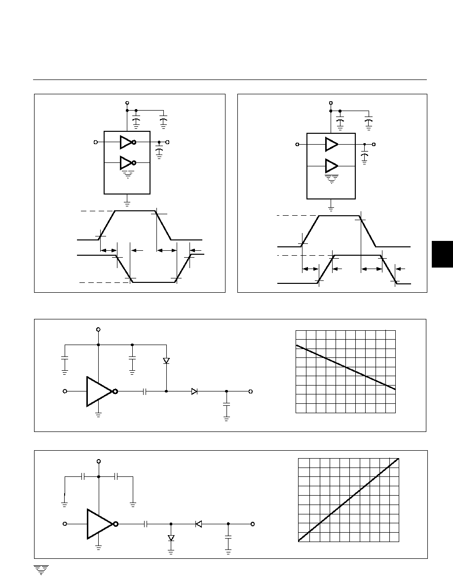
VOLTAGE INVERTER
+ 15V
0.1
µ
F 4.7
µ
F
10
µ
F
47
µ
F
+
≠
+
≠
1N4001
1N4001
VOUT
f = 10kHz
IN
2
6
3
7
1/2
TC426
+
≠
-6
-8
-10
-12
0
10 20 30 40 50 60 70 80 90
I (mA)
OUT
-7
-9
-11
-13
-5
-14
100
V (V)
OUT
+ 15V
0.1
µ
F
4.7
µ
F
10
µ
F
47
µ
F
+
≠
+
≠
+
≠
1N4001
1N4001
VOUT
f = 10kHz
IN
2
6
3
7
29.
27.
25.
23.
0
10
20 30 40 50 60 70 80 90
I (mA)
OUT
28.
26.
24.
22.
30.
100
V (V)
OUT
1/2
TC426
Test Figure 1. Inverting Driver Switching Time Test Circuit
Test Figure 2. Noninverting Driver Switching Time Test Circuit
VOLTAGE DOUBLER