 | –≠–ª–µ–∫—Ç—Ä–æ–Ω–Ω—ã–π –∫–æ–º–ø–æ–Ω–µ–Ω—Ç: TC4404EPA | –°–∫–∞—á–∞—Ç—å:  PDF PDF  ZIP ZIP |
Document Outline
- Return to Contents
- List of Figures
- 1. Switching Time Test Circuit
- Features
- Applications
- Ordering Information
- Functional Block Diagram
- General Description
- Absolute Maximum Ratings
- Electrical Characteristics
- Electrical Characteristics: Specifications measured over operating temperature range
- Circuit Layout Guidelines
- Pin Configurations (DIP AND SOIC)
- Typical Characteristics
4-219
TELCOM SEMICONDUCTOR, INC.
7
6
5
4
3
1
2
8
TC4404
TC4405
INPUT
GND
EFFECTIVE
INPUT
C 12 pF
300 mV
VDD
PULL UP
PULL DOWN
2 (3)
A (B)
8 (6)
7 (5)
4
1
TC4404
INVERTING
TC4405
NONINVERTING
4.7V
FEATURES
s
Independently-Programmable Rise and Fall Times
s
Low Output Impedance ................................ 7
Typ
s
High Speed t
R
, t
F
....... <30 nsec with 1000 pF Load
s
Short Delay Times .................................... < 30 nsec
s
Wide Operating Range .......................... 4.5V to 18V
s
Latch-Up Protected ......... Will Withstand >500 mA
Reverse Current (Either Polarity)
s
Input Withstands Negative Swings Up to ≠5V
APPLICATIONS
s
Motor Controls
s
Driving Bipolar Transistors
s
Driver for Nonoverlapping Totem Poles
s
Reach-Up/Reach-Down Driver
1.5A DUAL OPEN-DRAIN MOSFET DRIVERS
GENERAL DESCRIPTION
The TC4404 and TC4405 are CMOS buffer-drivers
constructed with complementary MOS outputs, where the
drains of the totem-pole output have been left separated so
that individual connections can be made to the pull-up and
pull-down sections of the output. This allows the insertion
of drain-current-limiting resistors in the pull-up and/or pull-
down sections, allowing the user to define the rates of rise
and fall for a capacitive load; or a reduced output swing, if
driving a resistive load, or to limit base current, when
driving a bipolar transistor. Minimum rise and fall times,
with no resistors, will be less than 30 nsec for a 1000-pF
load. There is no upper limit.
For driving MOSFETs in motor-control applications,
where slow-ON/fast-OFF operation is desired, these de-
vices are superior to the previously-used technique of add-
ing a diode-resistor combination between the driver output
and the MOSFET, because they allow accurate control of
turn-ON, while maintaining fast turn-OFF and maximum
noise immunity for an OFF device.
When used to drive bipolar transistors, these drivers
maintain the high speeds common to other TelCom driv-
ers. They allow insertion of a base current-limiting resistor,
while providing a separate half-output for fast turn-OFF. By
proper positioning of the resistor, either npn or pnp transis-
tors can be driven.
For driving many loads in low-power regimes, these
drivers, because they eliminate shoot-through currents in
the output stage, require significantly less power at higher
frequencies, and can be helpful in meeting low-power
budgets.
Because neither drain in an output is dependent on
the other, these devices can also be used as open-drain
buffer/drivers where both drains are available in one device,
ORDERING INFORMATION
Part No.
Package
Temperature
Range
TC4404COA
8-Pin SOIC
0
∞
C to +70
∞
C
TC4404CPA
8-Pin PDIP
0
∞
C to +70
∞
C
TC4404EOA
8-Pin SOIC
≠ 40
∞
C to +85
∞
C
TC4404EPA
8-Pin PDIP
≠ 40
∞
C to +85
∞
C
TC4404MJA
8-Pin CerDIP
≠ 55
∞
C to +125
∞
C
TC4405COA
8-Pin SOIC
0
∞
C to +70
∞
C
TC4405CPA
8-Pin PDIP
0
∞
C to +70
∞
C
TC4405EOA
8-Pin SOIC
≠ 40
∞
C to +85
∞
C
TC4405EPA
8-Pin PDIP
≠ 40
∞
C to +85
∞
C
TC4405MJA
8-Pin CerDIP
≠ 55
∞
C to +125
∞
C
FUNCTIONAL BLOCK DIAGRAM
TC4404/5-6 10/21/96

4-220
TELCOM SEMICONDUCTOR, INC.
ABSOLUTE MAXIMUM RATINGS
Supply Voltage ......................................................... +22V
Maximum Chip Temperature ................................. +150
∞
C
Storage Temperature Range ................ ≠ 65
∞
C to +150
∞
C
Lead Temperature (Soldering, 10 sec) ................. +300
∞
C
ELECTRICAL CHARACTERISTICS:
Specifications measured at T
A
= +25
∞
C with 4.5V
V
DD
18V, unless otherwise specified.
Symbol
Parameter
Test Conditions
Min
Typ
Max
Unit
Input
V
IH
Logic 1 High Input Voltage
2.4
--
--
V
V
IL
Logic 0 Low Input Voltage
--
--
0.8
V
I
IN
Input Current
≠ 0V
V
IN
V
DD
≠ 1
--
1
µ
A
Output
V
OH
High Output Voltage
V
DD
≠ 0.025
--
--
V
V
OL
Low Output Voltage
--
--
0.025
V
R
O
Output Resistance
I
OUT
= 10 mA, V
DD
= 18V; Any Drain
--
7
10
I
PK
Peak Output Current (Any Drain) Duty cycle < 2%, t
300
µ
sec
--
1.5
--
A
I
DC
Continuous Output Current (Any Drain)
--
--
100
mA
I
R
Latch-Up Protection (Any Drain)
Duty cycle < 2%, t
300
µ
sec
> 500
--
--
mA
Withstand Reverse Current
Switching Time (Note 1)
t
R
Rise Time
Figure 1, C
L
= 1000 pF
--
25
30
nsec
t
F
Fall Time
Figure 1, C
L
= 1000 pF
--
25
30
nsec
t
D1
Delay Time
Figure 1, C
L
= 1000 pF
--
15
30
nsec
t
D2
Delay Time
Figure 1, C
L
= 1000 pF
--
32
50
nsec
Power Supply
I
S
Power Supply Current
V
IN
= 3V (Both Inputs)
--
--
4.5
mA
V
IN
= 0V (Both Inputs)
--
--
0.4
NOTE:
1. Switching times guaranteed by design.
thus minimizing chip count. Unused open drains should be
returned to the supply rail that their device sources are
connected to (pull-downs to ground, pull-ups to V
DD
), to
prevent static damage. In addition, in situations where
timing resistors or other means of limiting crossover currents
are used, like drains may be paralleled for greater current
carrying capacity.
These devices are built to operate in the most de-
manding electrical environments. They will not latch up
under any conditions within their power and voltage rat-
ings; they are not subject to damage when up to 5V of
noise spiking of either polarity occurs on their ground pin;
and they can accept, without damage or logic upset, up to
1/2 amp of reverse current (of either polarity) being forced
back into their outputs. All terminals are fully protected
against up to 2 kV of electrostatic discharge.
Package Thermal Resistance
CerDIP R
J-A
............................................... 150
∞
C/W
CerDIP R
J-C
................................................. 55
∞
C/W
PDIP R
J-A
.................................................. 125
∞
C/W
PDIP R
J-C
.................................................... 45
∞
C/W
SOIC R
J-A
.................................................. 155
∞
C/W
SOIC R
J-C
.................................................... 45
∞
C/W
Operating Temperature Range
C Version ............................................... 0
∞
C to +70
∞
C
E Version .......................................... ≠ 40
∞
C to +85
∞
C
M Version ....................................... ≠ 55
∞
C to +125
∞
C
Package Power Dissipation (T
A
70
∞
C)
Plastic ............................................................. 730mW
CerDP ............................................................. 800mW
SOIC ............................................................... 470mW
*Static-sensitive device. Unused devices must be stored in conductive
material. Protect devices from static discharge and static fields. Stresses
above those listed under Absolute Maximum Ratings may cause perma-
nent damage to the device. These are stress ratings only and functional
operation of the device at these or any other conditions above those
indicated in the operational sections of the specifications is not implied.
Exposure to Absolute Maximum Rating Conditions for extended periods
may affect device reliability.
TC4404
TC4405
1.5A DUAL OPEN-DRAIN
MOSFET DRIVERS
4-221
TELCOM SEMICONDUCTOR, INC.
7
6
5
4
3
1
2
8
ELECTRICAL CHARACTERISTICS:
Specifications measured over operating temperature range
with 4.5V
V
DD
18V, unless otherwise specified.
Symbol
Parameter
Test Conditions
Min
Typ
Max
Unit
Input
V
IH
Logic 1 High Input Voltage
2.4
--
--
V
V
IL
Logic 0 Low Input Voltage
--
--
0.8
V
I
IN
Input Current
≠ 0V
V
IN
V
DD
≠ 10
--
10
µ
A
Output
V
OH
High Output Voltage
V
DD
≠ 0.025
--
--
V
V
OL
Low Output Voltage
--
--
0.025
V
R
O
Output Resistance
I
OUT
= 10 mA, V
DD
= 18V; Any Drain
--
9
12
I
PK
Peak Output Current (Any Drain) Duty cycle <2%, t
300
µ
sec
--
1.5
--
A
I
DC
Continuous Output Current (Any Drain)
--
--
100
mA
I
R
Latch-Up Protection (Any Drain)
Duty cycle <2%, t
300
µ
sec
>500
--
--
mA
Withstand Reverse Current
Switching Time (Note 1)
t
R
Rise Time
Figure 1, C
L
= 1000 pF
--
--
40
nsec
t
F
Fall Time
Figure 1, C
L
= 1000 pF
--
--
40
nsec
t
D1
Delay Time
Figure 1, C
L
= 1000 pF
--
--
40
nsec
t
D2
Delay Time
Figure 1, C
L
= 1000 pF
--
--
60
nsec
Power Supply
I
S
Power Supply Current
V
IN
= 3V (Both Inputs)
--
--
8
mA
V
IN
= 0V (Both Inputs)
--
--
0.6
NOTE
1. Switching times guaranteed by design.
PIN CONFIGURATIONS (DIP AND SOIC)
Circuit Layout Guidelines
Avoid long power supply and ground traces (added
inductance causes unwanted voltage transients). Use power
and ground planes wherever possible. In addition, it is
advisable that low ESR bypass capacitors (4.7
µ
F or 10
µ
F
1
8
2
7
3
6
4
5
TC4405
B BOTTOM
COM
IN B
IN A
VDD
B TOP
A BOTTOM
A TOP
1
8
2
7
3
6
4
5
TC4405
B BOTTOM
COM
IN B
IN A
VDD
B TOP
A BOTTOM
A TOP
1
8
2
7
3
6
4
5
TC4404
B BOTTOM
COM
IN B
IN A
VDD
B TOP
A BOTTOM
A TOP
1
8
2
7
3
6
4
5
TC4404
B BOTTOM
COM
IN B
IN A
VDD
B TOP
A BOTTOM
A TOP
tantalum) be placed as close to the driver as possible. The
driver should be physically located as close to the device it
is driving as possible to minimize the length of the output
trace.
TC4404
TC4405
1.5A DUAL OPEN-DRAIN
MOSFET DRIVERS
4-222
TELCOM SEMICONDUCTOR, INC.
TC4404
TC4405
1.5A DUAL OPEN-DRAIN
MOSFET DRIVERS
Figure 1. Switching Time Test Circuit
+5V
INPUT
10%
90%
10%
90%
10%
90%
18V
OUTPUT
tD1
tF
tR
tD2
0V
0V
90%
10%
10%
10%
tD1
tR
tD2
tF
90%
+5V
INPUT
18V
OUTPUT
0V
0V
90%
OUTPUT
INPUT
0.1
µ
F
VDD
C = 1000 pF
L
4.7
µ
F
= 18V
INVERTING DRIVER
4
2,3
8,7
1
NONINVERTING DRIVER
1
2
INPUT: 100 kHz, square wave,
tRISE = tFALL
10 nsec
4-223
TELCOM SEMICONDUCTOR, INC.
7
6
5
4
3
1
2
8
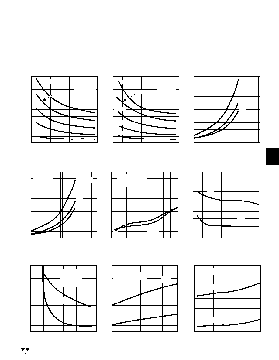
TYPICAL CHARACTERISTICS
Rise and Fall Times
vs. Temperature
Propagation Delay
vs. Supply Voltage
Fall Time vs. Supply Voltage
Rise Time vs. Supply Voltage
Fall Time vs. Capacitive Load
60
50
40
30
20
10
4
6
8
10
12
14
16
18
DELAY TIME (nsec)
tD2
tD1
CLOAD = 1000 pF
VDD
t RISE
(nsec)
4
6
8
10
12
14
16
18
VDD
100 pF
470 pF
2200 pF
1500 pF
100
80
60
40
20
0
1000 pF
TA = +25
∞
C
TIME (nsec)
t RISE
TEMPERATURE (
∞
C)
CLOAD = 1000 pF
60
50
40
30
20
10
≠55 ≠35
5
25 45 65 85 105 125
≠15
t FALL
VDD = 17.5V
t FALL
(nsec)
4
6
8
10
12
14
16
18
100 pF
470 pF
1000 pF
2200 pF
1500 pF
100
80
60
40
20
0
VDD
TA = +25
∞
C
Rise TIme vs. Capacitive Load
100
1000
10,000
CLOAD (pF)
VDD = 5V
10V
15V
t RISE
(nsec)
100
80
60
40
20
0
TA = +25
∞
C
t FALL
(nsec)
100
1000
10,000
100
80
60
40
20
0
CLOAD (pF)
VDD = 5V
TA = +25
∞
C
10V
15V
TA = +25
∞
C
Quiescent Supply Current
vs. Voltage
TEMPERATURE (
∞
C)
4
I QUIESCENT
(mA)
60
50
40
30
20
10
18
6
8
10
12
14
16
DELAY TIME (nsec)
VDRIVE (V)
60
50
40
30
20
10
DELAY TIME (nsec)
10
Effect of Input Amplitude
on Delay Time
Propagation Delay Time
vs. Temperature
≠55 ≠35 ≠15 5
25 45 65 85 105 125
CLOAD = 1000 pF
VDD = 10V
TA = +25
∞
C
VLOAD = 1000 pF
VDD = 17.5V
tD2
tD2
tD1
BOTH INPUTS = 1
BOTH INPUTS = 0
0
2
4
6
8
10
tD1
VDD
TA= +25
∞
C
1
0.1
TC4404
TC4405
1.5A DUAL OPEN-DRAIN
MOSFET DRIVERS