 | –≠–ª–µ–∫—Ç—Ä–æ–Ω–Ω—ã–π –∫–æ–º–ø–æ–Ω–µ–Ω—Ç: TC7109A | –°–∫–∞—á–∞—Ç—å:  PDF PDF  ZIP ZIP |
Document Outline
- Return to Contents
- List of Figures
- 1. TC7109A UART Interface (Send Any Word to UART to Transmit Latest Result)
- 2. TC7109A Parallel Interface With 8048/8049 Microcomputer
- 3. Conversion Timing (RUN/HOLD Pin High)
- 4. Digital Section
- 5. TC7109A RUN/HOLD Operation
- 6. TC7109A Direct Mode Output Timing
- 7. TC7109A Handshake With SEND INPUT Held Positive
- 8. TC7109A Handshake Ñ Typical UART Interface Timing
- 9. TC7109A Handshake Triggered by MODE Input
- 10. TC7109A RC Oscillator
- 11. TC7109A Crystal Oscillator
- 12. Direct Mode Chip and Byte Enable Combinations
- 13. Three-Stating Several TC7109A's to a Small Bus
- 14. Full-Time Parallel Interface to MCS-48, -80, -85 Microcomputers
- 15. Full-Time Parallel Interface to MCS-48, -80, -85 Microcomputers With Interrupt
- 16. Full-Time Parallel Interface to MC6800 or MCS650X Microprocessor
- 17. TC7109A Direct Interface to 8080/8085
- 18. TC7109A Direct Interface to MC6800 Bus
- 19. TC7109A Handshake Interface to MCS-48, -80, -85 Microcomputers
- 20. TC7109A Handshake Interface to MCS-6800, MCS650X Microprocessors
- 21. Handshake Interface for Multiplexed Converters
- 22. Normal Mode Rejection of Dual-Slope Converter as a Function of Frequency
- List of Tables
- 1. TC7109A Direct Mode Timing Requirements
- Features
- Ordering Information
- Functional Block Diagram
- General Description
- Absolute Maximum Ratings*
- Electrical Characteristics: All parameters with V + = +5V, V Ö = Ö5V, GND = 0V, TA = +25∞C,
- Pin Configurations
- TC7109/A Pin Description
- Detailed Description
- Analog Section
- Digital Section
- Oscillator
- Test Input
- Component Value Selection
- Interfacing
- Integrating Converter Features
3-91
TELCOM SEMICONDUCTOR, INC.
7
6
5
4
3
1
2
8
FEATURES
s
Zero-Integrator Cycle for Fast Recovery From
Input Overloads
s
Eliminates Cross -Talk in Multiplexed Systems
s
12-Bit Plus Sign Integrating A/D Converter With
Overrange Indication
s
Sign Magnitude Coding Format
s
True Differential Signal Input and Differential
Reference Input
s
Low Noise ............................................ 15
µ
V
P-P
Typ
s
Input Current .............................................. 1 pA Typ
s
No Zero Adjustment Needed
s
TTL-Compatible, Byte-Organized Tri-State
Outputs
s
UART Handshake Mode for Simple Serial Data
Transmission
ORDERING INFORMATION
PART CODE
TC7109X
A or blank*
Package
Temperature
Code
Package
Range
CKW
44-Pin PQFP
0
∞
C to +70
∞
C
CLW
44-Pin PLCC
0
∞
C to +70
∞
C
CPL
40-Pin Plastic DIP
0
∞
C to +70
∞
C
IJL
40-Pin CerDIP
≠25
∞
C to +85
∞
C
* The "A" version has a higher I
OUT
on the digital lines.
TC7109
TC7109A
12-BIT
µ
P-COMPATIBLE ANALOG-TO-DIGITAL CONVERTERS
GENERAL DESCRIPTION
The TC7109A is a 12-bit plus sign, CMOS low-power
analog-to-digital converter (ADC). Only eight passive com-
ponents and a crystal are required to form a complete
dual-slope integrating ADC.
The improved V
OH
source current TC7109A has fea-
tures that make it an attractive per-channel alternative to
analog multiplexing for many data acquisition applica-
tions. These features include typical input bias current of
1pA drift of less than 1
µ
V/
∞
C, input noise typically 15
µ
V
P-P
,
and auto-zero. True differential input and reference allow
measurement of bridge-type transducers such as load
cells, strain gauges, and temperature transducers.
The TC7109A provides a versatile digital interface. In
the direct mode, chip select and HIGH/LOW byte enables
control parallel bus interface. In the handshake mode, the
TC7109A will operate with industry-standard UARTs in
controlling serial data transmission -- ideal for remote
data logging. Control and monitoring of conversion timing
is provided by the RUN/HOLD input and STATUS output.
For applications requiring more resolution, see the
TC500, 15-bit plus sign ADC data sheet.
The TC7109A has improved overrange recovery per-
formance and higher output drive capability than the origi-
nal TC7109. All new (or existing) designs should specify
the TC7109A wherever possible.
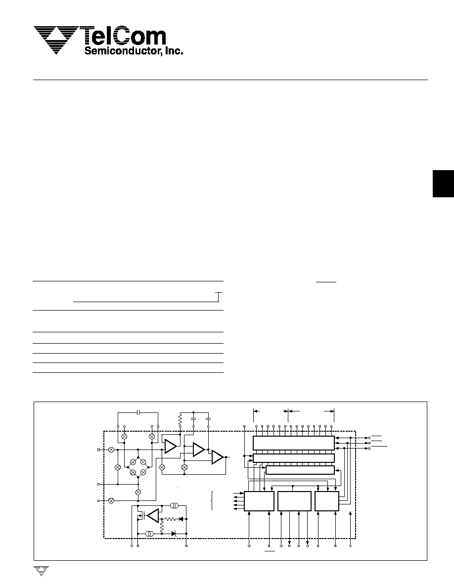
FUNCTIONAL BLOCK DIAGRAM
INPUT
HI
AZ
BUFF
CAZ
INT
BUFFER
INTEGRATOR
AZ
ZI
AZ
ZI
DE
(+)
AZ
INT
AZ
COMPARATOR
COMP
OUT
35
31
30
CREF
AZ
DE (
±
)
ZI
33
34
COMMON
INPUT
LO
INT
37
36
REF
IN
DE
(≠)
DE
(≠)
DE
(+)
RINT
CINT
38
39
REF
CAP
REF
CAP
ZI
6.2V
10
µ
A
28
40
V
+
V
≠
29
REF
OUT
17
3
4
5
6
7
8
9 10 11 12 13 14
2
26
22
23
24
25
21
TO
ANALOG
SECTION
COMP OUT
AZ
INT
DE (
±
)
ZI
CONVERSION
CONTROL
LOGIC
OSCILLATOR
AND CLOCK
CIRCUITRY
HANDSHAKE
LOGIC
15 16
27
18
19
20
LBEN
HBEN
CE/LOAD
1
GND
14 LATCHES
12-BIT COUNTER
16 THREE-STATE OUTPUTS
SEND
MODE
BUF
OSC
OUT
OSC
SEL
OSC
OUT
OSC
IN
RUN/
HOLD
STATUS
POL
OR
TEST
HIGH-ORDER
BYTE OUTPUTS
LOW-ORDER
BYTE OUTPUTS
TC7109A
+
+
REF
IN ≠
B
12
B
11
B
10
B
9
B
8
B
7
B
6
B
5
B
4
B
3
B
2
B
1
LATCH
CLOCK
32
≠
+
+
≠
≠
+
≠
TC7109/A-7 11/6/96

3-92
TELCOM SEMICONDUCTOR, INC.
ABSOLUTE MAXIMUM RATINGS*
Positive Supply Voltage (GND to V
+
) ..................... +6.2V
Negative Supply voltage (GND to V
≠
) ....................... ≠9V
Analog Input Voltage (Low to High) (Note 1) ....... V
+
to V
≠
Reference Input Voltage (Low to High (Note 1) .. V
+
to V
≠
Digital Input Voltage (Pins 2≠27) (Note 2) ..... GND ≠0.3V
Power Dissipation, T
A
< 70
∞
C, (Note 3)
CerDIP ............................................................. 2.29W
Plastic DIP ....................................................... 1.23W
PLCC ............................................................... 1.23W
PQFP ............................................................... 1.00W
Operating Temperature Range
Plastic Package (C) ............................... 0
∞
C to +70
∞
C
Ceramic Package (I) ....................... ≠ 25
∞
C to +85
∞
C
(M) ................... ≠ 55
∞
C to +125
∞
C
Storage Temperature Range ............... ≠ 65
∞
C to +150
∞
C
Lead Temperature (Soldering, 10 sec) ................. +300
∞
C
ELECTRICAL CHARACTERISTICS:
All parameters with V
+
= +5V, V
≠
= ≠5V, GND = 0V, T
A
= +25
∞
C,
unless otherwise indicated.
Symbol
Parameter
Test Conditions
Min
Typ
Max
Unit
Analog
Overload Recovery Time
--
0
1
Measurement
(TC7109A)
Cycle
Zero Input Reading
V
IN
= 0V
≠ 0000
8
±
0000
8
+0000
8
Octal Reading
Full Scale = 409.6 mV
Ratio Metric Reading
V
IN
= V
REF
3777
8
3777
8
4000
8
Octal Reading
V
REF
= 204.8 mV
4000
8
NL
Nonlinearity (Max Deviation
Full Scale = 409.6 mV to
≠1
±
0.2
+1
Count
From Best Straight Line Fit)
2.048V Over Full Operating
Temperature Range
Roll-Over Error (Difference in
Full Scale = 409.6 mV to
≠1
±
0.02
+1
Count
Reading for Equal Positive and
2.048V Over Full Operating
Negative Inputs Near (Full Scale)
Temperature Range
CMRR
Input Common-Mode
V
CM
±
1V, V
IN
= 0V
--
50
--
µ
V/V
Rejection Ratio
Full Scale = 409.6 mV
V
CMR
Common-Mode Voltage
Input High, Input Low,
V
≠
+1.5
--
V
+
≠1
V
Range
and Common Pins
e
N
Noise (P-P Value Not
V
IN
= 0V
--
15
--
µ
V
Exceeded 95% of Time)
Full Scale = 409.6 mV
I
IN
Leakage Current at Input
V
IN
, All Packages: +25
∞
C
--
1
10
pA
C Device: 0
∞
C
T
A
+70
∞
C
20
100
pA
I Device: ≠25
∞
C
T
A
+85
∞
C
100
250
pA
M Device: ≠55
∞
C
T
A
+125
∞
C
2
5
nA
TC
ZS
Zero Reading Drift
V
IN
= 0V
--
0.2
1
µ
V/
∞
C
TC
FS
Scale-Factor
V
IN
= 408.9 mV = >7770
8
--
1
5
µ
V/
∞
C
Temperature Coefficient
Reading, Ext Ref = 0 ppm/
∞
C
I
+
Supply Current
V
IN
= 0V, Crystal Oscillator
--
700
1500
µ
A
(V
+
to GND)
3.58 MHz Test Circuit
I
S
Supply Current (V
+
to V
≠
)
Pins 2≠21, 25, 26, 27, 29 Open
--
700
1500
µ
A
*Static-sensitive device. Unused devices must be stored in conductive
material. Protect devices from static discharge and static fields. Stresses
above those listed under Absolute Maximum Ratings may cause perma-
nent damage to the device. These are stress ratings only and functional
operation of the device at these or any other conditions above those
indicated in the operational sections of the specifications is not implied.
Exposure to Absolute Maximum Rating Conditions for extended periods
may affect device reliability.
NOTES: 1. Input voltages may exceed supply voltages if input current is
limited to
±
100
µ
A.
2. Connecting any digital inputs or outputs to voltages greater
than V
+
or less than GND may cause destructive device latch-
up. Therefore, it is recommended that inputs from sources
other than the same power supply should not be applied to
the TC7109A before its power supply is established. In
multiple supply systems, the supply to the device should be
activated first.
3. This limit refers to that of the package and will not occur during
normal operation.
TC7109
TC7109A
12-BIT
µ
P-COMPATIBLE
ANALOG-TO-DIGITAL CONVERTERS

3-93
TELCOM SEMICONDUCTOR, INC.
7
6
5
4
3
1
2
8
ELECTRICAL CHARACTERISTICS (Cont.)
Symbol
Parameter
Test Conditions
Min
Typ
Max
Unit
V
REF
Ref Out Voltage
Referenced to V
+
, 25 k
≠ 2.4
≠ 2.8
≠ 3.2
V
Between V
+
and Ref Out
TC
REF
Ref Out Temperature
25 k
Between V
+
and Ref Out
--
80
--
ppm/
∞
C
Coefficient
0
∞
C
T
A
+70
∞
C
Digital
V
OH
Output High Voltage
TC7109: I
OUT
= 100
µ
A
3.5
4.3
--
V
TC7109A: I
OUT
= 700
µ
A
Pins 3≠16, 18, 19, 20
V
OL
Output Low Voltage
I
OUT
= 1.6 mA
--
0.2
0.4
V
Output Leakage Current
Pins 3≠16 High Impedance
--
±
0.01
±
1
µ
A
Control I/O
Pins 18, 19, 20 V
OUT
= V
+
≠3V
--
5
--
µ
A
Pull-Up Current
Mode Input at GND
Control I/O Loading
HBEN, Pin 19; LBEN, Pin 18
--
--
50
pF
V
IH
Input High Voltage
Pins 18≠21, 26, 27
2.5
--
--
V
Referenced to GND
V
IL
Input Low Voltage
Pins 18-21, 26, 27
--
--
1
V
Referenced to GND
Input Pull-Up Current
Pins 26, 27; V
OUT
= V
+
≠3V
--
5
--
µ
A
Pins 17, 24; V
OUT
= V
+
≠3V
25
µ
A
Input Pull-Down Current
Pin 21; V
OUT
= GND = +3V
--
1
--
µ
A
Oscillator Output Current, High
V
OUT
= 2.5V
--
1
--
mA
Oscillator Output Current, Low
V
OUT
= 2.5V
--
1.5
--
mA
Buffered Oscillator Output
V
OUT
= 2.5V
--
2
--
mA
Current, High
Buffered Oscillator Output
V
OUT
= 2.5V
--
5
--
mA
Current, Low
t
W
Mode Input Pulse Width
60
--
--
nsec
HANDLING PRECAUTIONS: These devices are CMOS and must be handled correctly to prevent damage. Package
and store only in conductive foam, anti-static tubes, or other conducting material. Use proper anti-static handling
procedures. Do not connect in circuits under "power-on" conditions, as high transients may cause permanent
damage.
TC7109
TC7109A
12-BIT
µ
P-COMPATIBLE
ANALOG-TO-DIGITAL CONVERTERS
3-94
TELCOM SEMICONDUCTOR, INC.
TC7109
TC7109A
12-BIT
µ
P-COMPATIBLE
ANALOG-TO-DIGITAL CONVERTERS
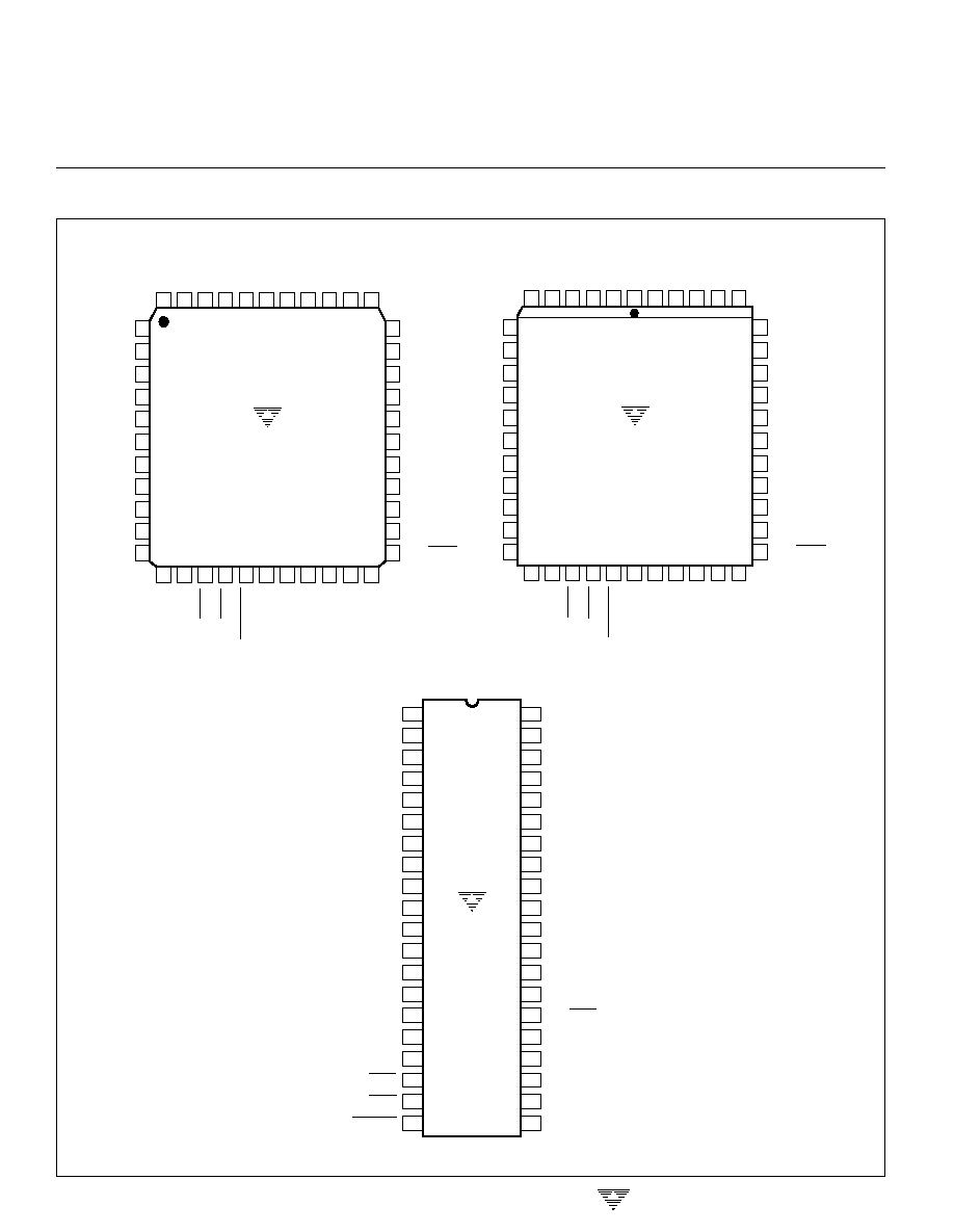
PIN CONFIGURATIONS
NC = NO INTERNAL CONNECTION
TC7109A
TC7109
(CPL, IJL,
MJL)
(PDIP)
(CerDIP)
1
2
3
4
5
6
7
8
9
10
11
12
STATUS
13
14
15
16
17
18
19
20
POL
OR
TEST
LBEN
HBEN
CE/LOAD
REF OUT
IN HI
IN LO
COMMON
V
+
SEND
RUN/HOLD
BUFF OSC OUT
OSC SEL
OSC IN
MODE
40
39
38
37
36
35
34
33
32
31
30
29
28
27
26
25
24
23
22
21
GND
OSC OUT
V
≠
BUFF
AZ
INT
REF IN
+
REF CAP
+
REF CAP
≠
REF IN
≠
12
B
11
B
10
B
9
B
8
B
7
B
6
B
5
B
4
B
3
B
2
B
1
B
27
28
29
30
31
32
33
7
4
3
2
1
INT
IN HI
12 13
14
15
17
18
1
BUFF
OSC OUT
AZ
NC
BUFF
44 43
42
41
39
38
40
GND
16
37
36
35
34
19
20
21
22
26
8
REF OUT
25
9
24
10
SEND
23
11
NC
5
6
B
TC7109ACKW
TC7109CKW
RUN/HOLD
V
≠
COMMON
IN LO
REF IN
+
REF CAP
+
REF CAP
≠
REF IN
≠
V
+
STATUS
POL
OR
9
B
11
B
10
B
8
B
7
B
NC
6
B
5
B
4
B
3
B
2
B
OSC SEL
OSC OUT
OSC IN
MODE
NC
CE/LOAD
HBEN
LBEN
TEST
12
B
(PQFP)
33
34
35
36
37
38
39
13
10
9
8
7
INT
IN HI
18 19
20
21
23
24
1
BUFF
OSC OUT
AZ
NC
BUFF
6
5
4
3
1
44
2
GND
22
43
42
41
40
25
26
27
28
32
14
REF OUT
31
15
30
16
SEND
29
17
NC
11
12
B
TC7109ACLW
TC7109CLW
(PLCC)
RUN/HOLD
V
≠
COMMON
IN LO
REF IN
+
REF CAP
+
REF CAP
≠
REF IN
≠
V
+
STATUS
POL
OR
9
B
11
B
10
B
8
B
7
B
NC
6
B
5
B
4
B
3
B
2
B
OSC SEL
OSC OUT
OSC IN
MODE
NC
CE/LOAD
HBEN
LBEN
TEST
12
B
3-95
TELCOM SEMICONDUCTOR, INC.
7
6
5
4
3
1
2
8
TC7109/A PIN DESCRIPTION
40-Pin PDIP
Pin Number
Symbol
Description
1
GND
Digital ground, 0V, ground return for all digital logic.
2
STATUS
Output HIGH during integrate and deintegrate until data is latched. Output LOW
when analog section is in auto-zero or zero-integrator configuration.
3
POL
Polarity -- High for positive input.
4
OR
Overrange -- High if overranged.
5
B
12
Bit 12 (Most Significant Bit)
6
B
11
Bit 11
7
B
10
Bit 10
8
B
9
Bit 9
9
B
8
Bit 8
10
B
7
Bit 7
11
B
6
Bit 6
12
B
5
Bit 5
13
B
4
Bit 4
14
B
3
Bit 3
15
B
2
Bit 2
16
B
1
Bit 1 (Least Significant Bit)
17
TEST
Input High -- Normal operation. Input LOW -- Forces all bit outputs HIGH.
Note: This input is used for test purposes only.
18
Low-Byte Enable -- With MODE (Pin 21) LOW, and CE/LOAD (Pin 20) LOW,
taking this pin LOW activates low-order byte outputs, B1≠B8. With MODE (Pin 21)
HIGH, this pin serves as low-byte flag output used in handshake mode. See
Figures 7, 8, and 9.
19
High-Byte Enable -- With MODE (Pin 21) LOW, and CE/LOAD (Pin 20) LOW,
taking this pin LOW activates high-order byte outputs, B9≠B12, POL, OR. With
MODE (Pin 21) HIGH, this pin serves as high-byte flag output used in handshake
mode. See Figures 7, 8, and 9.
20
Chip Enable/Load -- With MODE (Pin 21) LOW, CE/LOAD serves as a master
output enable. When HIGH, B1≠B12, POL, OR outputs are disabled. When
MODE (Pin 21) is HIGH, a load strobe is used in handshake mode. See Figure 7,
8, and 9.
21
MODE
Input LOW -- Direct output mode where CE/LOAD (Pin 20), HBEN (Pin 19), and
LBEN (Pin 18) act as inputs directly controlling byte outputs.
Input Pulsed HIGH -- Causes immediate entry into handshake mode and output
of data as in Figure 9.
Input HIGH -- Enables CE/LOAD (Pin 20), HBEN (Pin 19), and LBEN (Pin 18)
as outputs, handshake mode will be entered and data output as in Figures 7 and
8 at conversions completion.
22
OSC IN
Oscillator Input
23
OSC OUT
Oscillator Output
24
OSC SEL
Oscillator Select -- Input HIGH configures OSC IN, OSC OUT, BUF OSC OUT as
RC oscillator -- clock will be same phase and duty cycle as BUF OSC OUT. Input
LOW configures OSC IN, OSC OUT for crystal oscillator -- clock frequency will
be 1/58 of frequency at BUF OSC OUT.
25
BUF OSC OUT
Buffered Oscillator Output
26
Input HIGH -- Conversions continuously performed every 8192 clock pulses.
Input LOW -- Conversion in progress completed; converter will stop in auto-zero
seven counts before integrate.
HBEN
CE/LOAD
RUN/HOLD
All Three-State Data Bits
TC7109
TC7109A
12-BIT
µ
P-COMPATIBLE
ANALOG-TO-DIGITAL CONVERTERS
LBEN
3-96
TELCOM SEMICONDUCTOR, INC.
TC7109
TC7109A
12-BIT
µ
P-COMPATIBLE
ANALOG-TO-DIGITAL CONVERTERS
TC7109/A PIN DESCRIPTION (Cont.)
40-Pin PDIP
Pin Number
Symbol
Description
27
SEND
Input -- Used in handshake mode to indicate ability of an external device to
accept data.
Connect to V+ if not used.
28
V
≠
Analog Negative Supply -- Nominally ≠5V with respect to GND (Pin 1).
29
REF OUT
Reference Voltage Output -- Nominally 2.8V down from V
+
(Pin 40).
30
BUFFER
Buffer Amplifier Output
31
AUTO-ZERO
Auto-Zero Node -- Inside foil of C
AZ
.
32
INTEGRATOR
Integrator Output -- Outside foil of C
INT
.
33
COMMON
Analog Common -- System is auto-zeroed to COMMON.
34
INPUT LOW
Differential Input Low Side
35
INPUT HIGH
Differential Input High Side
36
REF IN +
Differential Reference Input Positive
37
REF CAP +
Reference Capacitor Positive
38
REF CAP ≠
Reference Capacitor Negative
39
REF IN ≠
Differential Reference Input Negative
40
V
+
Positive Supply Voltage -- Nominally +5V with respect to GND (Pin 1).
NOTE: All digital levels are positive true.
Figure 1. TC7109A UART Interface (Send Any Word to UART to Transmit Latest Result)
+
1
25
2
19
17
18
21
20
27
GND
BUFF OSC OUT
STATUS
HBEN
B1≠B8
TEST
LBEN
MODE
CE/LOAD
SEND
V
40
39
38
37
36
35
34
33
32
31
30
29
28
26
24
23
22
TC7109A
CLK
Q11
RESET
1
2
3
4
5≠12
13
14
15
16
V
OSC CONTROL
GND
RRD
RBR1≠8
PE
FE
OE
SFD
RR1
TRO
TRC
OSC IN
EPE
CLS1
CLS2
SBS
PI
CRL
*TBR1≠8
TRE
DRR
DR
TBRL
TBRE
MR
40
17
39
38
37
36
35
34
24
18
19
23
22
21
6403
CMOS UART
+5V
GND
+5V
GND
25
SERIAL
INPUT
20
SERIAL
OUTPUT
15
10
11
GND
GND
+5V
+5V
GND
+5V
≠5V
+5V OR OPEN
GND
3.58MHz
CRYSTAL
ANALOG
GND
EXTERNAL
REFERENCE
+
+
≠
INPUT
C
0.33
µ
F
AZ
C
0.15
µ
F
INT
0.01
µ
F
1M
1
µ
F
6
8
3≠8
9≠16
B9≠B12,
POL, OR
26≠33
For lowest power consumption, TBR1≠TBR8 inputs
should have 100k
pull-up resistors to +5V.
RINT
20k
100k
0.2V
1V
CD4040B
REF IN
≠
REF CAP
≠
REF CAP
+
REF IN
+
IN HI
IN LO
COM
INT
AZ
REF OUT
BUFF
V
≠
RUN/HOLD
OSC SEL
OSC OUT
OSC IN
REF
REF
8
≠
*
NOTE:
3-97
TELCOM SEMICONDUCTOR, INC.
7
6
5
4
3
1
2
8
Figure 2. TC7109A Parallel Interface With 8048/8049 Microcomputer
≠
40
1
17
V
GND
TEST
RUN/HOLD
STATUS
LBEN
HBEN
39
38
37
36
35
34
33
32
31
30
29
28
27
25
24
23
22
21
TC7109A
1
4
5
6
7
8
9
11
25
26
39
40
20
TO
RESET
SS
INT
EA
WR
PSEN
ALE
PROG
V
TL
V
GND
P20≠P27
2
8748/8049
CMOS
MICROCOMPUTER
+5V
OTHER I/O
+5V
GND
≠5V
GND
3.58MHz
CRYSTAL
ANALOG
GND
EXTERNAL
REFERNCE
+
+
≠
INPUT
C
0.33
µ
F
AZ
RINT
20k
10 k
0.2 V
1 V
XTAL2
XTALI
8
5
P14≠P17
P13
P12
P11
P10
DB0≠DB7
RD
30
29
28
27
B9≠B12,
POL, OR
B1≠B8
CE/LOAD
21≠24,
35≠38
12≠19
10
31≠34
26
2
18
19
C
0.15
µ
F
INT
0.01
µ
F
1M
1
µ
F
GND
+5V
+5V
+5V
+5V
GND
DD
CC
2
3
6
8
3≠8
9≠16
20
REF IN≠
REF CAP≠
REF CAP+
REF IN+
IN HI
HI LO
COM
INT
AZ
BUFF
REF OUT
V
OSC SEL
OSC OUT
OSC IN
SEND
BUFF OSC OUT
MODE
8
+
≠
REF
REF
Signal-Integrate Phase
The buffer and integrator inputs are removed from
common and connected to input high and input low. The
auto-zero loop is opened. The auto-zero capacitor is placed
in series in the loop to provide an equal and opposite
compensating offset voltage. The differential voltage be-
tween input high and input low is integrated for a fixed time
of 2048 clock periods. At the end of this phase, the polarity
of the integrated signal is determined. If the input signal has
no return to the converter's power supply, input low can be
tied to analog common to establish the correct common-
mode voltage.
Deintegrate Phase
Input high is connected across the previously-charged
reference capacitor and input low is internally connected to
analog common. Circuitry within the chip ensures the ca-
pacitor will be connected with the correct polarity to cause
the integrator output to return to the zero crossing (estab-
lished by auto-zero) with a fixed slope. The time, repre-
sented by the number of clock periods counted for the output
to return to zero, is proportional to the input signal.
DETAILED DESCRIPTION
(All Pin Designations Refer to 40-Pin DIP)
Analog Section
The functional diagram shows a block diagram of the
analog section of the TC7109A. The circuit will perform
conversions at a rate determined by the clock frequency
(8192 clock periods per cycle), when the RUN/HOLD input
is left open or connected to V
+
. Each measurement cycle is
divided into four phases, as shown in Figure 3. They are:
(1) Auto-Zero (AZ), (2) Signal Integrate (INT), (3) Reference
Deintegrate (DE), and (4) Zero Integrator (ZI).
Auto-Zero Phase
The buffer and the integrator inputs are disconnected
from input high and input low and connected to analog
common. The reference capacitor is charged to the refer-
ence voltage. A feedback loop is closed around the system
to charge the auto-zero capacitor, C
AZ
, to compensate for
offset voltage in the buffer amplifier, integrator, and com-
parator. Since the comparator is included in the loop, the AZ
accuracy is limited only by the noise of the system. The offset
referred to the input is less than 10
µ
V.
TC7109
TC7109A
12-BIT
µ
P-COMPATIBLE
ANALOG-TO-DIGITAL CONVERTERS

3-98
TELCOM SEMICONDUCTOR, INC.
TC7109
TC7109A
12-BIT
µ
P-COMPATIBLE
ANALOG-TO-DIGITAL CONVERTERS
reference for (+) or (≠) input voltages will cause a roll-over
error. This error can be held to less than 0.5 count worst case
by using a large reference capacitor in comparison to the
stray capacitance. To minimize roll-over error from these
sources, keep the reference common-mode voltage near or
at analog common.
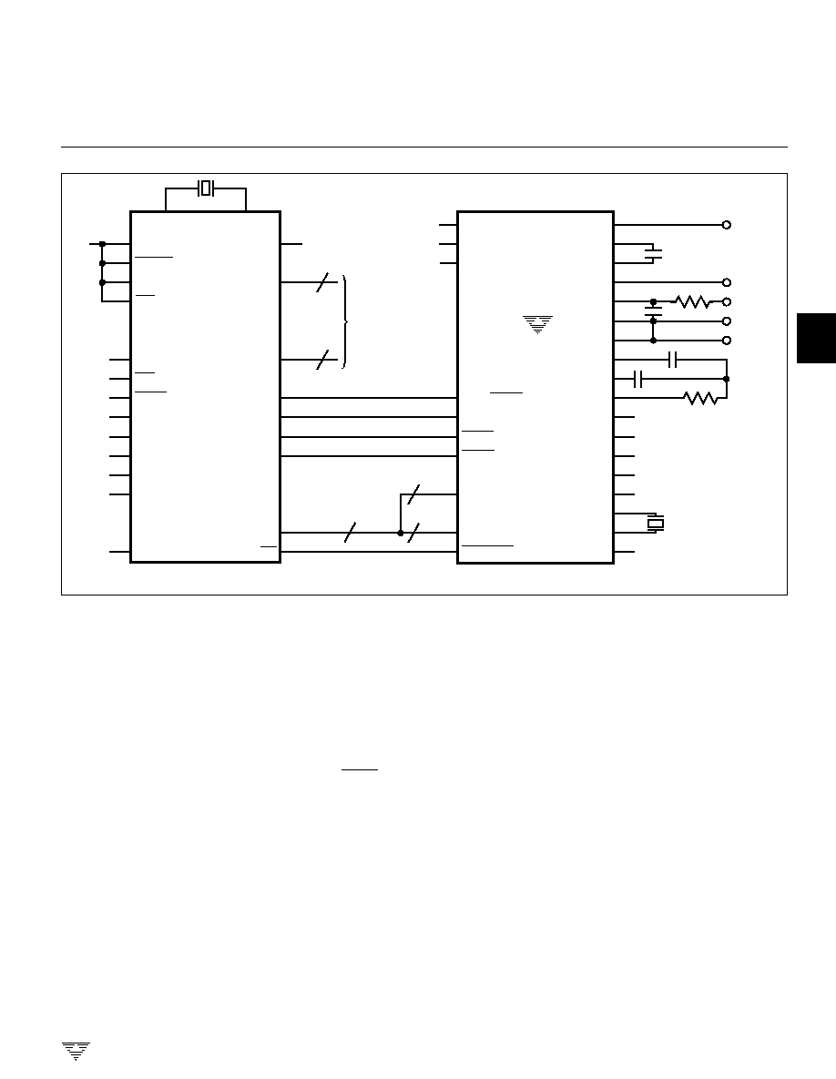
Digital Section
The digital section is shown in the block diagram (Fig-
ure 4) and includes the clock oscillator and scaling circuit,
a 12-bit binary counter with output latches and TTL com-
patible three-state output drivers, UART handshake logic,
polarity, overrange, and control logic. Logic levels are re-
ferred to as LOW or HIGH.
Inputs driven from TTL gates should have 3 k
to 5 k
pull-up resistors added for maximum noise immunity. For
minimum power consumption, all inputs should swing from
GND (LOW) to V
+
(HIGH).
STATUS Output
During a conversion cycle, the STATUS output goes
HIGH at the beginning of signal integrate and goes LOW
one-half clock period after new data from the conversion has
been stored in the output latches (see Figure 3). The signal
may be used as a "data valid" flag to drive interrupts, or for
monitoring the status of the converter. (Data will not change
while status is LOW.)
MODE Input
The output mode of the converter is controlled by the
MODE input. The converter is in its "direct" output mode,
when the MODE input is LOW or left open. The output data
is directly accessible under the control of the chip and byte
enable inputs (this input is provided with a pull-down resistor
to ensure a LOW Level when the pin is left open). When the
MODE input is pulsed high, the converter enters the UART
handshake mode and outputs the data in 2 bytes, then
returns to "direct" mode. When the MODE input is kept
HIGH, the converter will output data in the handshake mode
at the end of every conversion cycle. With MODE = 0 (direct
bus transfer), the send input should be tied to V
+
. (See
"Handshake Mode.")
RUN/HOLD Input
With the RUN/HOLD input high, or open, the circuit
operates normally as a dual-slope ADC, as shown in Figure
3. Conversion cycles operate continuously with the output
latches updated after zero crossing in the deintegrate mode.
An internal pull-up resistor is provided to ensure a HIGH
level with an open input.
Zero-Integrator Phase
The ZI phase only occurs when an input overrange
condition exists. The function of the ZI phase is to eliminate
residual charge on the integrator capacitor after an overrange
measurement. Unless removed, the residual charge will be
transferred to the auto-zero capacitor and cause an error in
the succeeding conversion.
The ZI phase virtually eliminates hysteresis or "cross
talk" in multiplexed systems. An overrange input on one
channel will not cause an error on the next channel mea-
sured. This feature is especially useful in thermocouple
measurements, where unused (or broken thermocouple)
inputs are pulled to the positive supply rail.
During ZI, the reference capacitor is charged to the
reference voltage. The signal inputs are disconnected from
the buffer and integrator. The comparator output is con-
nected to the buffer input, causing the integrator output to be
driven rapidly to 0V (Figure 3). The ZI phase only occurs
following an overrange and lasts for a maximum of 1024
clock periods.
Differential Input
The TC7109A has been optimized for operation with
analog common near digital ground. With +5V and ≠5V
power supplies, a full
±
4V full-scale integrator swing maxi-
mizes the analog section's performance.
A typical CMRR of 86 dB is achieved for input differential
voltages anywhere within the typical common-mode range
of 1V below the positive supply to 1.5V above the negative
supply. However, for optimum performance, the IN HI and IN
LO inputs should not come within 2V of either supply rail.
Since the integrator also swings with the common-mode
voltage, care must be exercised to ensure the integrator
output does not saturate. A worst-case condition is near a
full-scale negative differential input voltage with a large
positive common-mode voltage. The negative input signal
drives the integrator positive when most of its swing has
been used up by the positive common-mode voltage. In
such cases, the integrator swing can be reduced to less than
the recommended
±
4V full-scale value, with some loss of
accuracy. The integrator output can swing to within 0.3V of
either supply without loss of linearity.
Differential Reference
The reference voltage can be generated anywhere
within the power supply voltage of the converter. Roll-over
voltage is the main source of common-mode error, caused
by the reference capacitor losing or gaining charge due to
stray capacity on its nodes. With a large common-mode
voltage, the reference capacitor can gain charge (increase
voltage) when called upon to deintegrate a positive signal
and lose charge (decrease voltage) when called upon
to deintegrate a negative input signal. This difference in
3-99
TELCOM SEMICONDUCTOR, INC.
7
6
5
4
3
1
2
8
INTERNAL CLOCK
INTEGRATOR OUTPUT
FOR NORMAL INPUT
INTEGRATOR
SATURATES
INTERNAL LATCH
INTEGRATOR OUTPUT
FOR OVERRANGE INPUT
NO ZERO
CROSSING
ZI
AZ
ZERO INTEGRATOR
PHASE FORCES
INTEGRATOR
OUTPUT TO 0V
ZERO CROSSING
OCCURS
ZERO CROSSING
DETECTED
INT
PHASE II
STATUS OUTPUT
AZ
PHASE I
DE
PHASE III
AZ
FIXED
2048
COUNTS
2048
COUNTS
MIN
4096
COUNTS
MAX
NUMBER OF COUNTS TO ZERO CROSSING
PROPORTIONAL TO V
IN
AFTER ZERO CROSSING, ANALOG SECTION
WILL BE IN AUTO-ZERO CONFIGURATION
TEST
17
POL
3
OR
4
B
12
5
B
11
6
B
10
7
B
9
8
B
8
9
B
7
10
B
6
11
B
5
12
B
4
13
B
3
14
2
26
22
23
24
25
21
STATUS
RUN/
HOLD
OSC
IN
OSC
OUT
OSC
SEL
BUFF
OSC
OUT
MODE
TO
ANALOG
SECTION
COMP OUT
AZ
INT
DE (
±
)
ZI
CONVERSION
CONTROL
LOGIC
OSCILLATOR
AND CLOCK
CIRCUITRY
HIGH-ORDER
BYTE OUTPUTS
LOW-ORDER
BYTE OUTPUTS
HANDSHAKE
LOGIC
B
2
15
B
1
16
27
SEND
18
19
20
LBEN
HBEN
CE/LOAD
1
GND
14 LATCHES
12-BIT COUNTER
14 THREE-STATE OUTPUTS
LATCH
CLOCK
Figure 4. Digital Section
Figure 3. Conversion Timing (RUN/HOLD Pin High)
TC7109
TC7109A
12-BIT
µ
P-COMPATIBLE
ANALOG-TO-DIGITAL CONVERTERS
3-100
TELCOM SEMICONDUCTOR, INC.
TC7109
TC7109A
12-BIT
µ
P-COMPATIBLE
ANALOG-TO-DIGITAL CONVERTERS
Figure 5. TC7109A RUN/HOLD Operation
The RUN/HOLD input may be used to shorten conver-
sion time. If RUN/HOLD goes LOW any time after zero
crossing in the deintegrate mode, the circuit will jump to
auto-zero and eliminate that portion of time normally spent
in deintegrate.
If RUN/HOLD stays or goes LOW, the conversion will
complete with minimum time in deintegrate. It will stay in
auto-zero for the minimum time and wait in auto-zero for a
HIGH at the RUN/HOLD input. As shown in Figure 5, the
STATUS output will go HIGH 7 clock periods after RUN/
HOLD is changed to HIGH, and the converter will begin the
integrate phase of the next conversion.
The RUN/HOLD input allows controlled conversion in-
terface. The converter may be held at idle in auto-zero with
RUN/HOLD LOW. The conversion is started when RUN/
HOLD goes HIGH, and the new data is valid when the
STATUS output goes LOW (or is transferred to the UART;
see "Handshake Mode"). RUN/HOLD may now go LOW,
terminating deintegrate and ensuring a minimum auto-zero
time before stopping to wait for the next conversion. Conver-
sion time can be minimized by ensuring RUN/HOLD goes
LOW during deintegrate, after zero crossing, and goes
HIGH after the hold point is reached. The required activity on
the RUN/HOLD input can be provided by connecting it to the
buffered oscillator output. In this mode, the input value
measured determines the conversion time.
Direct Mode
The data outputs (bits 1 through 8, low-order bytes; bits
9 through 12, polarity and overrange high-order bytes) are
accessible under control of the byte and chip enable termi-
nals as inputs with the MODE pin at a LOW level. These
three inputs are all active LOW. Internal pull-up resistors are
provided for an inactive HIGH level when left open. When
chip enable is LOW, a byte-enable input LOW will allow the
outputs of the byte to become active. A variety of parallel
data accessing techniques may be used, as shown in the
"Interfacing" section. (See Figure 6 and Table 1.)
The access of data should be synchronized with the
conversion cycle by monitoring the STATUS output. This
prevents accessing data while it is being updated and
eliminates the acquisition of erroneous data.
Symbol
Description
Min
Typ
Max
Units
t
BEA
Byte Enable Width
200
500
nsec
t
DAB
Data Access Time
150
300
nsec
From Byte Enable
t
DHB
Data Hold Time
150
300
nsec
From Byte Enable
t
CEA
Chip Enable Width
300
500
nsec
t
DAC
Data Access Time
200
400
nsec
From Chip Enable
t
DHC
Data Hold Time
200
400
nsec
From Chip Enable
Table 1. TC7109A Direct Mode Timing Requirements
Figure 6. TC7109A Direct Mode Output Timing
INTEGRATOR OUTPUT
INTERNAL CLOCK
DETERMINATED
AT ZERO CROSSING
DETECTION
AUTO-ZERO
PHASE I
MIN 1790 COUNTS
MAX 2041 COUNTS
STATIC IN
HOLD STATE
INT
PHASE II
RUN/HOLD input is ignored until end of auto-zero phase.
*
NOTE:
*
INTERNAL LATCH
STATUS OUTPUT
RUN/HOLD INPUT
7 COUNTS
= HIGH IMPEDANCE
CE/LOAD
AS INPUT
tCEA
tBEA
HBEN
AS INPUT
tDAB
tDAB
LBEN
AS INPUT
HIGH-BYTE
DATA
LOW-BYTE
DATA
DATA
VALID
tDAC
tDHC
DATA
VALID
DATA
VALID

3-101
TELCOM SEMICONDUCTOR, INC.
7
6
5
4
3
1
2
8
Handshake Mode
An alternative means of interfacing the TC7109A to
digital systems is provided when the handshake output
mode of the TC7109A becomes active in controlling the
flow of data instead of passively responding to chip and
byte enable inputs. This mode allows a direct interface
between the TC7109A and industry-standard UARTs with
no external logic required. The TC7109A provides all the
control and flag signals necessary to sequence the two
bytes of data into the UART and initiate their transmission
in serial form when triggered into the handshake mode.
The cost of designing remote data acquisition stations is
reduced using serial data transmission to minimize the
number of lines to the central controlling processor.
The MODE input controls the handshake mode. When
the MODE input is held HIGH, the TC7109A enters the
handshake mode after new data has been stored in the
output latches at the end of every conversion performed
(see Figures 7 and 8). Entry into the handshake mode may
be triggered on demand by the MODE input. At any time
during the conversion cycle, the LOW-to-HIGH transition of
a short pulse at the MODE input will cause immediate entry
into the handshake mode. If this pulse occurs while new
data is being stored, the entry into handshake mode is
delayed until the data is stable. The MODE input is ignored
in the handshake mode, and until the converter completes
the output cycle and clears the handshake mode, data
updating will be inhibited (see Figure 9).
When the MODE input is HIGH or when the converter
enters the handshake mode, the chip and byte enable
inputs become TTL-compatible outputs which provide the
output cycle control signals (see Figures 7, 8 and 9).
The SEND input is used by the converter as an indica-
tion of the ability of the receiving device (such as a UART)
to accept data in the handshake mode. The sequence of
the output cycle with SEND held HIGH is shown in Figure
7. The handshake mode (internal MODE HIGH) is entered
after the data latch pulse (the CE/LOAD, LBEN and HBEN
terminals are active as outputs since MODE remains HIGH).
The HIGH level at the SEND input is sensed on the
same HIGH-to-LOW internal clock edge. On the next LOW-
to-HIGH internal clock edge, the high-order byte (bits 9
through 12, POL, and OR) outputs are enabled and the CE/
LOAD and the HBEN outputs assume a LOW level. The
CE/LOAD output remains LOW for one full internal clock
period only; the data outputs remain active for 1-1/2 inter-
nal clock periods; and the high-byte enable remains LOW
for 2 clock periods. The CE/LOAD output LOW level or
LOW-to-HIGH edge may be used as a synchronizing sig-
nal to ensure valid data, and the byte enable as an output
may be used as a byte identification flag. With SEND
remaining HIGH the converter completes the output cycle
using CE/LOAD and LBEN while the low-order byte out-
puts (bits 1 through 8) are activated. When both bytes are
sent, the handshake mode is terminated. The typical UART
interfacing timing is shown in Figure 8. The SEND input is
used to delay portions of the sequence, or handshake, to
ensure correct data transfer. This timing diagram shows an
industry-standard HD6403 or CDP1854 CMOS UART to
interface to serial data channels. The SEND input to the
TC7109A is driven by the TBRE (Transmitter Buffer Regis-
ter Empty) output of the UART, and the CE/LOAD input of
the TC7109A drives the TBRL (Transmitter Buffer Register
Load) input to the UART. The eight transmitter buffer regis-
ter inputs accept the parallel data outputs. With the UART
transmitter buffer register empty, the SEND input will be
HIGH when the handshake mode is entered after new data
is stored. The high-order byte outputs become active and
the CE/LOAD and HBEN inputs will go LOW after SEND is
sensed. When CE/LOAD goes HIGH at the end of one
clock period, the high-order byte data is clocked into the
UART transmitter buffer register. The UART TBRE output
will go LOW, which halts the output cycle with the HBEN
output LOW, and the high-order byte outputs active. When
the UART has transferred the data to the transmitter regis-
ter and cleared the transmitter buffer register, the TBRE
returns HIGH. The high-order byte outputs are disabled on
the next TC7109A internal clock HIGH-to-LOW edge, and
one-half internal clock later, the HBEN output returns HIGH.
The CE/LOAD and LBEN outputs go LOW at the same
time as the low-order byte outputs become active. When
the CE/LOAD returns HIGH at the end of one clock period,
the low-order data is clocked into the UART transmitter
buffer register, and TBRE again goes LOW. The next
TC7109A internal clock HIGH-to-LOW edge will sense
when TBRE returns to a HIGH, disabling the data inputs.
One-half internal clock later, the handshake mode is cleared,
and the CE/LOAD, HBEN and LBEN terminals return
HIGH and stay active, if MODE still remains HIGH.
Handshake output sequences may be performed on
demand by triggering the converter into handshake mode
with a LOW-to-HIGH edge on the MODE input. A hand-
shake output sequence triggered is shown in Figure 9. The
SEND input is LOW when the converter enters handshake
mode. The whole output sequence is controlled by the
SEND input, and the sequence for the first (high order) byte
is similar to the sequence for the second byte.
Figure 9 also shows that the output sequence can take
longer than a conversion cycle. New data will not be latched
when the handshake mode is still in progress and is there-
fore lost.
TC7109
TC7109A
12-BIT
µ
P-COMPATIBLE
ANALOG-TO-DIGITAL CONVERTERS

3-102
TELCOM SEMICONDUCTOR, INC.
TC7109
TC7109A
12-BIT
µ
P-COMPATIBLE
ANALOG-TO-DIGITAL CONVERTERS
Figure 8. TC7109A Handshake -- Typical UART Interface Timing
Figure 7. TC7109A Handshake With SEND INPUT Held Positive
= THREE-STATE
HIGH IMPEDANCE
INTEGRATOR
OUTPUT
DATA VALID
DATA VALID
INTERNAL CLOCK
INTERNAL LATCH
STATUS OUTPUT
MODE INPUT
INTERNAL MODE
SEND INPUT
CE/LOAD
HBEN
HIGH-BYTE DATA
LBEN
LOW-BYTE DATA
= DON'T CARE
= THREE-STATE
WITH PULL-UP
UART
NORM
TERMINATES
UART MODE
ZERO CROSSING DETECTED
ZERO CROSSING OCCURS
SEND SENSED
SEND SENSED
MODE LOW,
NOT IN
HANDSHAKE
MODE
DISABLES
OUTPUTS
CE/LOAD,
HBEN,
LBEN
MODE HIGH ACTIVATES
CE/LOAD, HBEN, LBEN
= THREE-STATE HIGH IMPEDANCE
INTEGRATOR OUTPUT
DATA VALID
INTERNAL CLOCK
INTERNAL LATCH
STATUS OUTPUT
MODE INPUT
INTERNAL MODE
SEND INPUT (UART TBRE)
CE/LOAD OUTPUT (UART TBRL)
HBEN
HIGH-BYTE DATA
LBEN
LOW-BYTE DATA
= DON'T CARE
UART
NORM
TERMINATES
UART MODE
ZERO CROSSING DETECTED
ZERO CROSSING OCCURS
SEND
SENSED
SEND
SENSED
SEND
SENSED
DATA VALID

3-103
TELCOM SEMICONDUCTOR, INC.
7
6
5
4
3
1
2
8
Figure 9. TC7109A Handshake Triggered by MODE Input
DATA VALID
DATA VALID
TERMINATES
UART MODE
= THREE-STATE
HIGH IMPEDANCE
INTERNAL CLOCK
INTERNAL LATCH
STATUS OUTPUT
MODE INPUT
INTERNAL MODE
SEND INPUT
CE/LOAD AS OUTPUT
HBEN
HIGH-BYTE DATA
LBEN
LOW-BYTE DATA
= DON'T CARE
= THREE-STATE
WITH PULL-UP
UART
NORM
SEND
SENSED
SEND
SENSED
ZERO CROSSING DETECTED
ZERO CROSSING OCCURS
STATUS OUTPUT UNCHANGED
IN UART MODE
LATCH PULSE INHIBITED
IN UART MODE
POSITIVE TRANSITION
CAUSES ENTRY INTO
UART MODE
DE PHASE III
SEND
SENSED
Oscillator
The oscillator may be overdriven, or may be operated as
an RC or crystal oscillator. The OSCILLATOR SELECT
input optimizes the internal configuration of the oscillator for
RC or crystal operation. The OSCILLATOR SELECT input
is provided with a pull-up resistor. When the OSCILLATOR
SELECT input is HIGH or left open, the oscillator is config-
ured for RC operation. The internal clock will be the same
frequency and phase as the signal at the BUFFERED
OSCILLATOR OUTPUT. Connect the resistor and capaci-
tor as in Figure 10. The circuit will oscillate at a frequency
given by f = 0.45/RC. A 100 k
resistor is recommended for
useful ranges of frequency. The capacitor value should be
chosen such that 2048 clock periods are close to an integral
multiple of the 60 Hz period for optimum 60 Hz line rejection.
With OSCILLATOR SELECT input LOW, two on-chip
capacitors and a feedback device are added to the oscillator.
In this configuration, the oscillator will operate with most
crystals in the 1 to 5 MHz range with no external components
(Figure 11). The OSCILLATOR SELECT input LOW inserts
a fixed 58 divider circuit between the BUFFERED OSCIL-
LATOR OUTPUT and the internal clock. A 3.58 MHz TV
crystal gives a division ratio providing an integration time
given by:
t = (2048 clock periods) = 33.18 ms
The error is less than 1% from two 60 Hz periods, or
33.33 ms, which will give better than 40 dB, 60 Hz rejection.
The converter will operate reliably at conversion rates up
to 30 per second, corresponding to a clock frequency of
245.8 kHz.
When the oscillator is to be overdriven, the OSCILLA-
TOR OUTPUT should be left open, and the overdriving
signal should be applied at the OSCILLATOR INPUT. The
internal clock will be of the same duty cycle, frequency and
phase as the input signal. When the OSCILLATOR SELECT
is at GND, the clock will be 1/58 of the input frequency.
58
3.58 MHz
TC7109
TC7109A
12-BIT
µ
P-COMPATIBLE
ANALOG-TO-DIGITAL CONVERTERS
3-104
TELCOM SEMICONDUCTOR, INC.
roll-over errors will be slightly worse than in the
±
4V case.
For large common-mode voltage ranges, the integrator
output swing must be reduced further. This will increase both
noise and roll-over errors. To improve performance,
±
6V
supplies may be used.
Integrating Capacitor
The integrating capacitor, C
INT
, should be selected to
give the maximum integrator output voltage swing that will
not saturate the integrator to within 0.3V from either supply.
A
±
3.5V to
±
4V integrator output swing is nominal for the
TC7109A, with
±
5V supplies and analog common con-
nected to GND. For 7-1/2 conversions per second (61.72
kHz internal clock frequency), nominal values C
INT
and C
AZ
are 0.15
µ
F and 0.33
µ
F, respectively. These values should
be changed if different clock frequencies are used to main-
tain the integrator output voltage swing. The value of C
INT
is
given by:
C
INT
=
The integrating capacitor must have low dielectric ab-
sorption to prevent roll-over errors. Polypropylene capaci-
tors give undetectable errors, at reasonable cost, up to
+85
∞
C. Teflon
Æ
capacitors are recommended for the military
temperature range. While their dielectric absorption charac-
teristics vary somewhat between units, devices may be
selected to less than 0.5 count of error due to dielectric
absorption.
Integrating Resistor
The integrator and buffer amplifiers have a class A
output stage with 100
µ
A of quiescent current. They supply
20
µ
A of drive current with negligible nonlinearity. The
integrating resistor should be large enough to remain in this
very linear region over the input voltage range, but small
enough that undue leakage requirements are not placed on
the PC board. For 2.048V full-scale a 100 k
resistor is
recommended and for 409.6 mV full-scale a 20 k
resistor
is recommended. R
INT
may be selected for other values of
full scale by:
R
INT
=
Figure 10. TC7109A RC Oscillator
23
OSC
OUT
25
BUFFERED
OSC OUT
24
OSC
SEL
V OR OPEN
+
22
OSC
IN
R
C
f = 0.45/RC
OSC
Figure 11. TC7109A Crystal Oscillator
23
OSC
OUT
25
BUFFERED
OSC OUT
24
OSC
SEL
GND
V
+
22
OSC
IN
58
CLOCK
CRYSTAL
˜
Test Input
The counter and its outputs may be tested easily. When
the TEST input is connected to GND, the internal clock is
disabled and the counter outputs are all forced into the HIGH
state. When the input returns to the 1/2 (V
+
≠GND) voltage or
to V
+
and one clock is input, the counter outputs will all be
clocked to the LOW state.
The counter output latches are enabled when the TEST
input is taken to a level halfway between V
+
and GND,
allowing the counter contents to be examined anytime.
Component Value Selection
The integrator output swing for full-scale should be as
large as possible. For example, with
±
5V supplies and
COMMON connected to GND, the nominal integrator output
swing at full-scale is
±
4V. Since the integrator output can go
to 0.3V from either supply without significantly effecting
linearity, a 4V integrator output swing allows 0.7V for varia-
tions in output swing due to component value and oscillator
tolerances. With
±
5V supplies and a common-mode voltage
range of
±
1V required, the component values should be
selected to provide
±
3V integrator output swing. Noise and
(2048 Clock Period) (20
µ
A)
Integrator Output Voltage Swing
Full-Scale Voltage
20
µ
A
Auto-Zero Capacitor
As the auto-zero capacitor is made large, the system
noise is reduced. Since the TC7109A incorporates a zero
integrator cycle, the size of the auto-zero capacitor does not
affect overload recovery. The optimal value of the auto-zero
capacitor is between 2 and 4 times C
INT
. A typical value for
C
AZ
is 0.33
µ
F.
TC7109
TC7109A
12-BIT
µ
P-COMPATIBLE
ANALOG-TO-DIGITAL CONVERTERS

3-105
TELCOM SEMICONDUCTOR, INC.
7
6
5
4
3
1
2
8
The inner foil of C
AZ
should be connected to pin 31 and
the outer foil to the RC summing junction. The inner foil of
C
INT
should be connected to the RC summing junction and
the outer foil to pin 32 for best rejection of stray pickups. For
low leakage at temperatures above +85
∞
C, use Teflon
capacitors.
Reference Capacitor
A 1
µ
F capacitor is recommended for most circuits.
However, where a large common-mode voltage exists, a
larger value is required to prevent roll-over error (e.g., the
reference low is not analog common), and a 409.6 mV scale
is used. The roll-over error will be held to 0.5 count with a 10
µ
F capacitor. For temperatures above +80
∞
C use Teflon or
equivalent capacitors for their low leakage characteristics.
Reference Voltage
To generate full-scale output of 4096 counts, the analog
input required is V
IN
= 2 V
REF
. For 409.6 mV full scale, use
a reference of 204.8 mV. In many applications, where the
ADC is connected to a transducer, a scale factor will exist
between the input voltage and the digital reading. For
instance, in a measuring system, the designer might like to
have a full-scale reading when the voltage for the transducer
is 700 mV. Instead of dividing the input down to 409.6 mV,
the designer should use the input voltage directly and select
V
REF
= 350 mV. Suitable values for integrating resistor and
capacitor would be 34 k
and 0.15
µ
F. This makes the
system slightly quieter and also avoids a divider network on
the input. Another advantage of this system occurs when
temperature and weight measurements with an offset or tare
are desired for non-zero input. The offset may be introduced
by connecting the voltage output of the transducer between
common and analog high, and the offset voltage between
common and analog low, observing polarities carefully. In
processor-based systems using the TC7109A, it may be
more desirable to use software and perform this type of
scaling or tare subtraction digitally.
Reference Sources
A major factor in the absolute accuracy of the ADC is the
stability of the reference voltage. The 12-bit resolution of the
TC7109A is one part in 4096, or 244 ppm. Thus, for the on-
board reference temperature coefficient of 70 ppm/
∞
C, a
temperature difference of 3
∞
C will introduce a one-bit abso-
lute error. Where the ambient temperature is not controlled,
or where high-accuracy absolute measurements are being
made, it is recommended that an external high-quality
reference be used.
A reference output (pin 29) is provided which may be
used with a resistive divider to generate a suitable reference
voltage (20 mA may be sunk without significant variation in
output voltage). A pull-up bias device is provided which
sources about 10
µ
A. The output voltage is nominally 2.8V
below V
+
. When using the on-board reference, REF OUT
(pin 29) should be connected to REF
≠
(pin 39), and REF
+
should be connected to the wiper of a precision potentiom-
eter between REF OUT and V
+
. The test circuit shows the
circuit for a 204.8 mV reference, generated by a 2 k
precision potentiometer in series with a 24 k
fixed resistor.
Interfacing
Direct Mode
Combinations of chip-enable and byte-enable control
signals which may be used when interfacing the TC7109A
to parallel data lines are shown in Figure 12. The CE/LOAD
input may be tied low, allowing either byte to be controlled
by its own enable (Figure 12A). Figure 12B shows the
HBEN and LBEN as flag inputs, and CE/LOAD as a master
enable, which could be the READ strobe available from
most microprocessors. Figure 12C shows a configuration
where the two byte enables are connected together. The
CE/LOAD is a chip enable, and the HBEN and LBEN may
be used as a second chip enable, or connected to ground.
The 14 data outputs will be enabled at the same time. In
the direct MODE, SEND should be tied to V
+
.
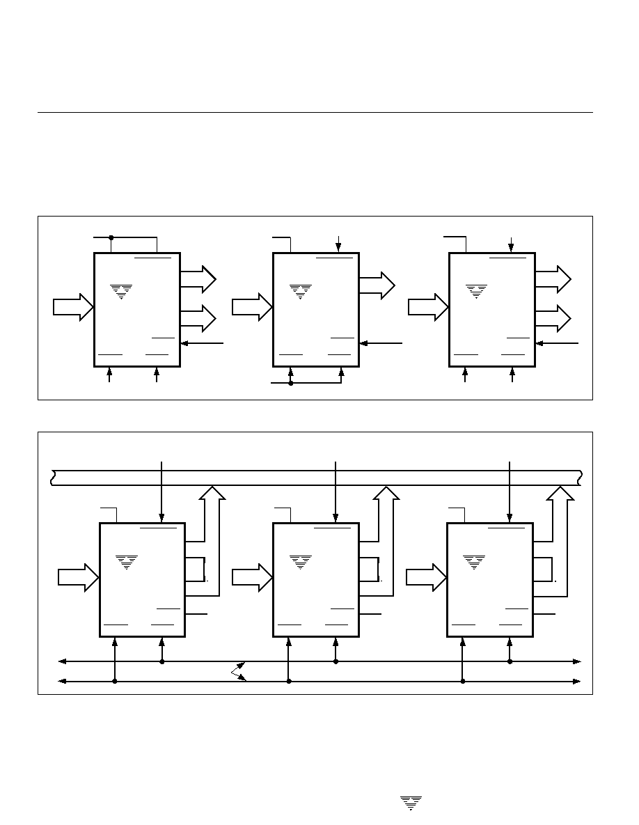
Figure 13 shows interfacing several TC7109A's to a
bus, ganging the HBEN and LBEN signals to several con-
verters together, and using the CE/LOAD input to select
the desired converter.
Figures 14≠19 give practical circuits utilizing the paral-
lel three-state output capabilities of the TC7109A. Figure
14 shows parallel interface to the Intel MCS-48, -80 and -
85 systems via an 8255 PPI, where the TC7109A data
outputs are active at all times. The 8155 I/O ports may be
used in an identical manner. This interface can be used in a
read-after-update sequence, as shown in Figure 15. The
data is accessed by the high-to-low transition of the STA-
TUS driving an interrupt to the microprocessor.
The RUN/HOLD input is also used to initiate conver-
sions under software control. Figure 16 gives an interface
to Motorola MC6800 or MOS Technology MCS650X sys-
tem.
An interrupt is generated through the Control Register
B, CB1 line from the high-to-low transition of the STATUS
output. The RUN/HOLD pin is controlled by CB2 through
Control Register B, allowing software control of conver-
sions.
TC7109
TC7109A
12-BIT
µ
P-COMPATIBLE
ANALOG-TO-DIGITAL CONVERTERS
3-106
TELCOM SEMICONDUCTOR, INC.
Direct interfacing to most microprocessor busses is
easily accomplished through the three-state output of the
TC7109A.
Figures 1, 17 and 18 are typical connection diagrams.
To ensure requirements for setup and hold times, minimum
pulse widths, and the drive limitations on long busses are
met, it is necessary to carefully consider the system timing
in this type of interface. This type of interface is used when
the memory peripheral address density is low, providing
simple address decoding. Interrupt handling can be simpli-
fied by using an interface to reduce the component count.
TC7109A
MODE
CE/LOAD
B9≠B12
POL, OR
B1≠B8
LBEN
HBEN
GND
8
ANALOG
IN
6
CONVERT
CONTROL
RUN/HOLD
TC7109A
MODE
CE/LOAD
B1≠B12
POL, OR
LBEN
HBEN
GND
ANALOG
IN
CONVERT
RUN/HOLD
TC7109A
MODE
CE/LOAD
B9≠B12
POL, OR
B1≠B8
LBEN
HBEN
8
ANALOG
IN
6
CONVERT
RUN/HOLD
CHIP SELECT 1
GND OR
CHIP SELECT 2
14
BYTE FLAGS
GND
CHIP SELECT
A.
B.
C.
Figure 12. Direct Mode Chip and Byte Enable Combinations
TC7109A
MODE
CE/LOAD
B9≠B12
POL, OR
B1≠B8
LBEN
HBEN
GND
8
ANALOG
IN
6
RUN/HOLD
+5V
CONVERTER
SELECT
TC7109A
MODE
CE/LOAD
B9≠B12
POL, OR
B1≠B8
LBEN
HBEN
GND
8
ANALOG
IN
6
RUN/HOLD
+5V
TC7109A
MODE
CE/LOAD
B9≠B12
POL, OR
B1≠B8
LBEN
HBEN
GND
8
ANALOG
IN
6
RUN/HOLD
+5V
CONVERTER
SELECT
CONVERTER
SELECT
BYTE SELECT FLAGS
Figure 13. Three-Stating Several TC7109A's to a Small Bus
TC7109
TC7109A
12-BIT
µ
P-COMPATIBLE
ANALOG-TO-DIGITAL CONVERTERS

3-107
TELCOM SEMICONDUCTOR, INC.
7
6
5
4
3
1
2
8
TC7109A
MODE
CE/LOAD
B9≠B12
POL, OR
B1≠B8
STATUS
RUN/HOLD
LBEN
HBEN
GND
GND
8
6
SEE TEXT
8255
(MODE 0)
RD WR
D7≠D0
A0≠A1
CS
PA5≠PA0
PB7≠PB0
PC5
87C48
8008, 8080,
8085, 8048, ETC.
DATA BUS
CONTROL BUS
ADDRESS BUS
ANALOG
IN
+5V
Figure 14. Full-Time Parallel Interface to MCS-48, -80, -85 Microcomputers
TC7109A
MODE
CE/LOAD
B9≠B12
POL, OR
B1≠B8
STATUS
RUN/HOLD
LBEN
HBEN
GND
GND
8
6
+5V
(SEE TEXT)
1
µ
F
8255
RD WR
D7≠D0
PC6
A0≠A1
CS
PA5≠PA0
PB7≠PB0
PC4
STBA
PC6
INTR
87C48
8008, 8080,
8085, 8048, ETC.
DATA BUS
CONTROL BUS
ADDRESS BUS
INTRA
ANALOG
IN
10k
Figure 15. Full-Time Parallel Interface to MCS-48, -80, -85 Microcomputers With Interrupt
TC7109
TC7109A
12-BIT
µ
P-COMPATIBLE
ANALOG-TO-DIGITAL CONVERTERS
3-108
TELCOM SEMICONDUCTOR, INC.
TC7109
TC7109A
12-BIT
µ
P-COMPATIBLE
ANALOG-TO-DIGITAL CONVERTERS
TC7109A
MODE
B9≠B12
POL, OR
B1≠B8
STATUS
LBEN
ANALOG
IN
HBEN
GND
GND
8
6
MC6820
PA≠5
PB≠7
CB2
MC6800
OR
MCS650X
CONTROL
BUS
ADDRESS
BUS
CE/
LOAD
RUN/HOLD
CB1
DATA
BUS
CRB - -11R-01
Figure 16. Full-Time Parallel Interface to MC6800 or MCS650X Microprocessor
TC7109A
B9≠B12
POL, OR
B1≠B8
RUN/HOLD
MODE
8
6
8008, 8080, 8085
DATA BUS
CONTROL BUS
ADDRESS BUS
ANALOG
IN
RD
A15
A14
CE/LOAD
LBEN
HBEN
+5V
GND
*
MEMR or IOR for 8080/8228 system.
*
Figure 17. TC7109A Direct Interface to 8080/8085

3-109
TELCOM SEMICONDUCTOR, INC.
7
6
5
4
3
1
2
8
TC7109
TC7109A
12-BIT
µ
P-COMPATIBLE
ANALOG-TO-DIGITAL CONVERTERS
TC7109A
MODE
B9≠B12
POL, OR
B1≠B8
ANALOG
IN
CE/LOAD
GND
8
6
MC6800
OR
MCS650X
CONTROL
BUS
ADDRESS
BUS
HBEN
DATA
BUS
74C42
74C30
RUN/HOLD
+5V
LBEN
A0≠A2
A15≠A10
R/W, VMA
Figure 18. TC7109A Direct Interface to MC6800 Bus
TC7109A
B9≠B12
POL, OR
B1≠B8
CE/LOAD
SEND
RUN/HOLD
MODE
8
6
8255
(MODE 1)
RD WR
D7≠D0
PC
A0≠A1
CS
PA7≠PA0
PC4
PC5
PC6
PC7
INTR
87C48
8008, 8080,
8085, 8048, ETC.
DATA BUS
CONTROL BUS
ADDRESS BUS
ANALOG
IN
STBA
PC3
IBFA
Figure 19. TC7109A Handshake Interface to MCS-48, -80, -85 Microcomputers

3-110
TELCOM SEMICONDUCTOR, INC.
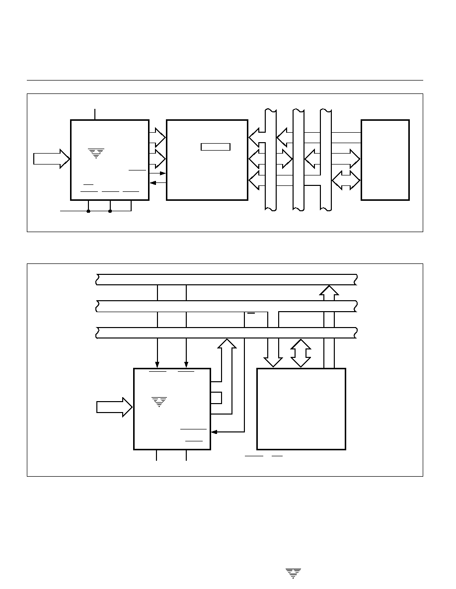
Handshake Mode
The handshake mode provides an interface to a wide
variety of external devices. The byte enables may be used
as byte identification flags or as load enables and external
latches may be clocked by the rising edge of CE/LOAD. A
handshake interface to Intel microprocessors using an 8255
PPI is shown in Figure 19. The handshake operation with
the 8255 is controlled by inverting its Input Buffer Full (IBF)
flag to drive the SEND input to the TC7109A, and using the
CE/LOAD to drive the 8255 strobe. The internal control
register of the PPI should be set in MODE 1 for the port
used. If the 8255 IBF flag is LOW and the TC7109A is in
handshake mode, the next word will be strobed into the
port. The strobe will cause IBF to go HIGH (SEND goes
LOW), which will keep the enabled byte outputs active. The
PPI will generate an interrupt which, when executed, will
result in the data being read. The IBF will be reset LOW
when the byte is read, causing the TC7109A to sequence
into the next byte. The MODE input to the TC7109A is
connected to the control line on the PPI.
The data from every conversion will be sequenced in
two bytes in the system, if this output is left HIGH, or tied
HIGH separately. (The data access must take less time
than a conversion.) The output sequence can be obtained
on demand if this output is made to go from LOW to HIGH
and the interrupt may be used to reset the MODE bit.
Conversions may be obtained on command under soft-
ware control by driving the RUN/HOLD input to the TC7109A
by a bit of the 8255. Another peripheral device may be
serviced by the unused port of the 8255. The 8155 may be
used in a similar manner. The MCS650X microprocessors
are shown in Figure 20 with MODE and RUN/HOLD tied
HIGH to save port outputs.
The handshake mode is particularly useful for directly
interfacing to industry-standard UARTs (such as Western
Digital TR1602), providing a means of serially transmitting
converted data with minimum component count.
A typical UART connection is shown in Figure 1. In this
circuit, any word received by the UART causes the UART
DR (Data Ready) output to go HIGH. The MODE input to
the TC7109A goes HIGH, triggering the TC7109A into
handshake mode. The high-order byte is output to the
UART and when the UART has transferred the data to the
Transmitter register, TBRE (SEND) goes HIGH again, LBEN
will go HIGH, driving the UART DRR (Data Ready Reset)
which will signal the end of the transfer of data from the
TC7109A to the UART.
An extension of the typical connection to several
TC7109A's with one UART is shown in Figure 21. In this
circuit, the word received by the UART (available at the
RBR outputs when DR is HIGH) is used to select which
converter will handshake with the UART. Up to eight
TC7109A's may interface with one UART, with no external
components. Up to 256 converters may be accessed on
one serial line with additional components.
TC7109A
MODE
SEND
ANALOG
IN
HBEN
+5V
CA2
MC6800
OR
MCS650X
CONTROL
BUS
ADDRESS
BUS
CE/LOAD
CA1
DATA
BUS
MC6820
CRA - -100-01
LBEN
RUN/HOLD
PA0≠PA7
Figure 20. TC7109A Handshake Interface to MCS-6800, MCS650X Microprocessors
TC7109
TC7109A
12-BIT
µ
P-COMPATIBLE
ANALOG-TO-DIGITAL CONVERTERS

3-111
TELCOM SEMICONDUCTOR, INC.
7
6
5
4
3
1
2
8
TC7109A
B9≠B12
POL, OR
B1-B8
LBEN
HBEN
8
6
ANALOG
IN
RUN/HOLD
SEND
MODE CE/
LOAD
+5V
TC7109A
B9≠B12
POL, OR
B1≠B8
LBEN
HBEN
8
6
8-BIT DATA BUS
ANALOG
IN
RUN/HOLD
SEND
MODE CE/
LOAD
+5V
TC7109A
B9≠B12
POL, OR
B1≠B8
LBEN
HBEN
8
6
ANALOG
IN
RUN/HOLD
SEND
MODE CE/
LOAD
+5V
TBRL DRR
GND
TBRE
RBR1≠RBR8
SFD
TBR1≠TBR8
SERIAL OUTPUT
SERIAL INPUT
6402 CMOS UART
2
3
Figure 21. Handshake Interface for Multiplexed Converters
Integrating Converter Features
The output of integrating ADCs represents the integral,
or average, of an input voltage over a fixed period of time.
Compared with techniques in which the input is sampled and
held, the integrating converter averages the effects of noise.
A second important characteristic is that time is used to
quantize the answer, resulting in extremely small nonlinearity
errors and no missing output codes. The integrating con-
verter also has very good rejection of frequencies whose
periods are an integral multiple of the measurement period.
This feature can be used to advantage in reducing line
frequency noise (Figure 22).
30
20
10
0
0.1/t
1/t
10/t
INPUT FREQUENCY
NORMAL MODE REJECTION PLAN
t = MEASUREMENT
PERIOD
Figure 22. Normal Mode Rejection of Dual-Slope Converter as a
Function of Frequency
TC7109
TC7109A
12-BIT
µ
P-COMPATIBLE
ANALOG-TO-DIGITAL CONVERTERS