 | –≠–ª–µ–∫—Ç—Ä–æ–Ω–Ω—ã–π –∫–æ–º–ø–æ–Ω–µ–Ω—Ç: TC7126CPL | –°–∫–∞—á–∞—Ç—å:  PDF PDF  ZIP ZIP |
Document Outline
- Return to Contents
- List of Figures
- 1. Basic Dual-Slope Converter
- 2. Normal-Mode Rejection of Dual-Slope Converter
- 3. TC7126A Block Diagram
- 4. Display Font and Segment Assignment
- 5. Common-Mode Voltage Removed in Battery Operation With VIN = Analog Common
- 6. Common-Mode Voltage Reduces Available Integrator
- 7. Analog Common Temperature
- 8. TC7126A Internal Voltage Reference Connection
- 9. Decimal Point and Annunciator Drives
- 10. Low Parts Count Ratiometric Resistance Measurement
- 11. 3-1/2 Digit True RMS AC DMM
- 12. Temperature Sensor
- 13. Positive Temperature Coefficient Resistor
- 14. Integrated Circuit Temperature Sensor
- Features
- Typical Applications
- Typical Operating Circuit
- General Description
- Ordering Information
- Available Packages
- Absolute Maximum Ratings*
- Electrical Characteristics
- Pin Configurations
- Pin Description
- Pin Description (Cont.)
- General Theory of Operation
- Dual-Slope Conversion Principles
- Analog Section
- Auto-Zero Phase
- Signal Integration Phase
- Reference Integrate Phase
- Digital Section
- Component Value Selection
- Auto-Zero Capacitor
- Reference Voltage Capacitor
- Integrating Capacitor
- Integrating Resistor
- Oscillator Components
- Reference Voltage Selection
- Device Functional Description
- Differential Signal Inputs
- Differential Reference
- TC7126A Internal Voltage Reference
- Applications Information
- Liquid Crystal Display Sources
- Decimal Point and Annunciator Drive
- Flat Package
- Ratiometric Resistance Measurements

3-217
TELCOM SEMICONDUCTOR, INC.
7
6
5
4
3
1
2
8
TC7126
TC7126A
3-1/2 DIGIT ANALOG-TO-DIGITAL CONVERTERS
FEATURES
s
Low Temperature Drift Internal Reference
TC7126 ....................................... 80 ppm/
∞
C Typ
TC7126A ..................................... 35 ppm/
∞
C Typ
s
Guaranteed Zero Reading With Zero Input
s
Low Noise .................................................... 15
µ
V
P-P
s
High Resolution .............................................. 0.05%
s
Low Input Leakage Current ...................... 1 pA Typ
10 pA Max
s
Precision Null Detectors With True Polarity at
Zero
s
High-Impedance Differential Input
s
Convenient 9V Battery Operation With
Low Power Dissipation ........................ 500
µ
W Typ
900
µ
W Max
TYPICAL APPLICATIONS
s
Thermometry
s
Bridge Readouts: Strain Gauges, Load Cells, Null
Detectors
s
Digital Meters and Panel Meters
-- Voltage/Current/Ohms/Power, pH
s
Digital Scales, Process Monitors
GENERAL DESCRIPTION
The TC7126A is a 3-1/2 digit CMOS analog-to-digital
converter (ADC) containing all the active components nec-
essary to construct a 0.05% resolution measurement sys-
tem. Seven-segment decoders, digit and polarity drivers,
voltage reference, and clock circuit are integrated on-chip.
The TC7126A directly drives a liquid crystal display (LCD),
and includes a backplane driver.
A low-cost, high-resolution indicating meter requires
only a display, four resistors, and four capacitors. The
TC7126A's extremely low power drain and 9V battery
operation make it ideal for portable applications.
The TC7126A reduces linearity error to less than 1
count. Roll-over error (the difference in readings for equal
magnitude but opposite polarity input signals) is below
±
1
count. High-impedance differential inputs offer 1 pA leak-
age current and a 10
12
input impedance. The 15
µ
V
P-P
noise performance guarantees a "rock solid" reading, and
the auto-zero cycle guarantees a zero display reading with
a 0V input.
The TC7126A features a precision, low-drift internal
voltage reference and is functionally identical to the TC7126.
A low-drift external reference is not normally required with
the TC7126A.
ORDERING INFORMATION
PART CODE
TC7126X X XXX
A or blank*
R (reversed pins) or blank (CPL pkg only)
* "A" parts have an improved reference TC
Package Code (see below):
Package
Temperature
Code
Package
Range
CKW
44-Pin PQFP
0
∞
C to +70
∞
C
CLW
44-Pin PLCC
0
∞
C to +70
∞
C
CPL
40-Pin PDIP
0
∞
C to +70
∞
C
IPL
40-Pin PDIP (non-A only)
≠ 25
∞
C to +85
∞
C
V
REF
+
TC7126
TC7126A
33
34
240 k
10 k
31
29
39
38
40
V
REF
≠
0.33
µF
0.1 µF
V
≠
1
OSC
3
OSC
2
OSC
TO ANALOG COMMON
(PIN 32)
1 CONVERSION/SEC
COSC
560 k
180 k
0.15 µF
0.01 µF
ANALOG
INPUT
+
≠
C
REF
≠
C
REF
+
V
IN
+
V
IN
≠
ANALOG
COMMON
V
INT
V
BUFF
C
AZ
20
21
1
SEGMENT
DRIVE
2≠19
22≠25
POL
BP
V
+
MINUS SIGN
BACKPLANE
28
50 pF
LCD
1 M
27
30
32
35
36
9V
+
ROSC
26
NOTE: Pin numbers refer to 40-pin DIP.
40-Pin Plastic DIP
44-Pin Plastic Quad Flat
Package Formed Leads
44-Pin Plastic Chip
Carrier PLCC
AVAILABLE PACKAGES
TYPICAL OPERATING CIRCUIT
TC7126/A-8 11/6/96
3-218
TELCOM SEMICONDUCTOR, INC.
3-1/2 DIGIT
ANALOG-TO-DIGITAL CONVERTERS
TC7126
TC7126A
ABSOLUTE MAXIMUM RATINGS*
Supply Voltage (V
+
to V
≠
) ......................................... +15V
Analog Input Voltage (Either Input) (Note 1) ........ V
+
to V
≠
Reference Input Voltage (Either Input) ................. V
+
to V
≠
Clock Input ...................................................... TEST to V
+
Operating Temperature Range
C Devices .............................................. 0
∞
C to +70
∞
C
I Devices ........................................... ≠ 25
∞
C to +85
∞
C
Storage Temperature Range ................ ≠ 65
∞
C to +150
∞
C
Lead Temperature (Soldering, 10 sec) ................. +300
∞
C
Power Dissipation, (T
A
70
∞
C), (Note 2)
44-Pin PQFP .................................................... 1.00W
44-Pin PLCC ..................................................... 1.23W
40-Pin Plastic PDIP .......................................... 1.23W
*Static-sensitive device. Unused devices must be stored in conductive
material. Protect devices from static discharge and static fields. Stresses
above those listed under Absolute Maximum Ratings may cause perma-
nent damage to the device. These are stress ratings only and functional
operation of the device at these or any other conditions above those
indicated in the operational sections of the specifications is not implied.
Exposure to Absolute Maximum Rating Conditions for extended periods
may affect device reliability.
ELECTRICAL CHARACTERISTICS:
V
S
= +9V, f
CLK
= 16 kHz, and T
A
= +25
∞
C, unless otherwise noted.
Symbol
Parameter
Test Conditions
Min
Typ
Max
Unit
Input
Zero Input Reading
V
IN
= 0V
≠000.0
±
000.0
+000.0
Digital
Full Scale = 200 mV
Reading
Zero Reading Drift
V
IN
= 0V, 0
∞
C
T
A
+70
∞
C
--
0.2
1
µ
V/
∞
C
Ratiometric Reading
V
IN
= V
REF
, V
REF
= 100 mV
999
999/1000
1000
Digital
Reading
NL
Linearity Error
Full Scale = 200 mV or 2V
≠ 1
±
0.2
1
Count
Max Deviation From Best Fit
Straight Line
Roll-Over Error
≠V
IN
= +V
IN
200 mV
≠ 1
±
0.2
1 Count
e
N
Noise
V
IN
= 0V, Full Scale = 200 mV
--
15
--
µ
V
P-P
I
L
Input Leakage Current
V
IN
= 0V
--
1
10
pA
CMRR
Common-Mode Rejection
V
CM
=
±
1V, V
IN
= 0V,
--
50
--
µ
V/V
Ratio
Full Scale = 200 mV
Scale Factor Temperature
V
IN
= 199 mV, 0
∞
C
T
A
+70
∞
C
--
1
5
ppm/
∞
C
Coefficient
Ext Ref Temp Coeff = 0 ppm/
∞
C
Analog Common
V
CTC
Analog Common
250 k
Between Common and V
+
--
--
--
--
Temperature Coefficient
0
∞
C
T
A
+70
∞
C ("C" Devices):
--
--
--
--
TC7126
--
80
--
ppm/
∞
C
TC7126A
--
35
75
ppm/
∞
C
≠ 25
∞
C
T
A
+85
∞
C ("I" Device):
TC7126A
--
35
100
ppm/
∞
C
V
C
Analog Common Voltage
250 k
Between Common and V
+
2.7
3.05
3.35
V
LCD Drive
V
SD
LCD Segment Drive Voltage
V
+
to V
≠
= 9V
4
5
6
V
P-P
V
BD
LCD Backplane Drive Voltage
V
+
to V
≠
= 9V
4
5
6
V
P-P
Power Supply
I
S
Power Supply Current
V
IN
= 0V, V
+
to V
≠
= 9V (Note 6)
--
55
100
µ
A
NOTES: 1. Input voltage may exceed supply voltages when input current is limited to 100
µ
A.
2. Dissipation rating assumes device is mounted with all leads soldered to PC board.
3. Refer to "Differential Input" discussion.
4. Backplane drive is in-phase with segment drive for "OFF" segment and 180
∞
out-of-phase for "ON" segment. Frequency is 20 times
conversion rate. Average DC component is less than 50 mV.
5. See "Typical Operating Circuit."
6. During auto-zero phase, current is 10≠20
µ
A higher. A 48 kHz oscillator increases current by 8
µ
A (typical). Common current not
included.

3-219
TELCOM SEMICONDUCTOR, INC.
7
6
5
4
3
1
2
8
3-1/2 DIGIT
ANALOG-TO-DIGITAL CONVERTERS
TC7126
TC7126A
PIN CONFIGURATIONS
27
28
29
30
31
32
33
7
4
3
2
1
NC
TC7126CKW
TC7126ACKW
(FLAT PACKAGE)
12
13
14
15
17
18
G
44
43
42
41
39
38
40
COMMON
16
37
C
AZ
36
V
BUFF
35
V
INT
34
V
19
20
21
22
D
26
8
+
25
9
24
10
23
11
5
6
C
OSC
TEST
NC
NC
V
3
3
D
2
C
2
B
2
A
2
F
2
E
2
NC
OSC2
OSC1
REF
C
REF
C
≠
2
3
A3
G3
BP
POL
AB4
E3
F3
B3
33
34
35
36
37
38
39
13
10
9
8
7
COMMON
VREF
18
19
20
21
23
24
3
AB
4
POL
NC
BP
NC
B
6
5
4
3
1
44
2
A
OSC
22
43
OSC
42
OSC
41
TEST
40
25
26
27
28
F
E
G
A
C
G
32
14
CAZ
2
31
15
VBUFF
2
30
16
VINT
E
29
17
D
NC
11
12
NC
C
D
3
2
F
A
2
2
2
B
3
3
3
3
3
2
TC7126CLW
TC7126ACLW
(PLCC)
1
2
3
V
≠
1
B
1
C
1
D
1
V
+
F1
G1
E1
D1
C1
B1
A
1
F
1
G
1
E
1
+
≠
REF
C
REF
C
+
≠
≠
+
VIN
VIN
≠
V
REF
+
V
REF
+
V
REF
≠
+
V
IN
V
IN
≠
TC7126CPL
TC7126ACPL
TC7126IPL
TC7126AIPL
1
2
3
4
OSC1
5
6
7
8
9
10
11
12
TEST
V
ANALOG
COMMON
CAZ
V+
D
NORMAL PIN
CONFIGURATION
13
14
15
16
17
18
19
20
40
39
38
37
36
35
34
33
32
31
30
29
28
27
26
25
24
23
22
21
2
C2
B2
A2
F2
E2
D3
B3
F3
E3
AB4
10's
100's
1000's
100's
OSC2
OSC3
+
REF
V
≠
REF
C
+
REF
C
≠
REF
V
+
IN
V
≠
IN
VBUFF
VINT
V ≠
G
C
A
G
BP
(BACKPLANE)
POL
(MINUS SIGN)
3
3
3
2
TC7126RCPL
TC7126ARCPL
TC7126RIPL
TC7126ARIPL
1
2
3
4
5
6
7
8
9
10
11
12
13
14
15
16
17
18
19
20
100's
1000's
100's
REVERSE PIN
CONFIGURATION
40
39
38
37
36
35
34
33
32
31
30
29
28
27
26
25
24
23
22
21
D1
C1
B1
A1
F1
G1
E1
1's
V+
D2
C2
B2
A2
F2
E2
D3
B3
F3
E3
AB4
POL
(MINUS SIGN)
D1
C1
B1
A1
F1
G1
E1
1's
10's
OSC
TEST
V
ANALOG
COMMON
CAZ
OSC2
OSC
+
REF
V
≠
REF
C
+
REF
C
≠
REF
V
+
IN
V
≠
IN
VBUFF
VINT
V ≠
G
C
A
G
BP
(BACKPLANE)
3
3
3
2
3
1
NC = NO INTERNAL CONNECTION

3-220
TELCOM SEMICONDUCTOR, INC.
3-1/2 DIGIT
ANALOG-TO-DIGITAL CONVERTERS
TC7126
TC7126A
PIN DESCRIPTION
40-Pin PDIP
Pin Number
Normal
(Reverse)
Name
Description
1
(40)
V
+
Positive supply voltage.
2
(39)
D
1
Activates the D section of the units display.
3
(38)
C
1
Activates the C section of the units display.
4
(37)
B
1
Activates the B section of the units display.
5
(36)
A
1
Activates the A section of the units display.
6
(35)
F
1
Activates the F section of the units display.
7
(34)
G
1
Activates the G section of the units display.
8
(33)
E
1
Activates the E section of the units display.
9
(32)
D
2
Activates the D section of the tens display.
10
(31)
C
2
Activates the C section of the tens display.
11
(30)
B
2
Activates the B section of the tens display.
12
(29)
A
2
Activates the A section of the tens display.
13
(28)
F
2
Activates the F section of the tens display.
14
(27)
E
2
Activates the E section of the tens display.
15
(26)
D
3
Activates the D section of the hundreds display.
16
(25)
B
3
Activates the B section of the hundreds display.
17
(24)
F
3
Activates the F section of the hundreds display.
18
(23)
E
3
Activates the E section of the hundreds display.
19
(22)
AB
4
Activates both halves of the 1 in the thousands display.
20
(21)
POL
Activates the negative polarity display.
21
(20)
BP
Backplane drive output.
22
(19)
G
3
Activates the G section of the hundreds display.
23
(18)
A
3
Activates the A section of the hundreds display.
24
(17)
C
3
Activates the C section of the hundreds display.
25
(16)
G
2
Activates the G section of the tens display.
26
(15)
V
≠
Negative power supply voltage.
27
(14)
V
INT
The integrating capacitor should be selected to give the maximum voltage swing
that ensures component tolerance build-up will not allow the integrator output to
saturate. When analog common is used as a reference and the conversion rate is
3 readings per second, a 0.047
µ
F capacitor may be used. The capacitor must
have a low dielectric constant to prevent roll-over errors. See "Integrating Capaci-
tor" section for additional details.
28
(13)
V
BUFF
Integration resistor connection. Use a 180 k
resistor for a 200 mV full-scale
range and a 1.8 M
resistor for a 2V full-scale range.
29
(12)
C
AZ
The size of the auto-zero capacitor influences system noise. Use a 0.33
µ
F
capacitor for 200 mV full scale, and a 0.033
µ
F capacitor for 2V full scale. See
paragraph on auto-zero capacitor for more details.
30
(11)
V
IN
≠
The low input signal is connected to this pin.
31
(10)
V
IN
+
The high input signal is connected to this pin.
32
(9)
ANALOG
This pin is primarily used to set the analog common-mode voltage for battery
operation or in systems where the input signal is referenced to the power supply.
See paragraph on analog common for more details. It also acts as a reference
voltage source.
33
(8)
C
REF
≠
See pin 34.
COMMON

3-221
TELCOM SEMICONDUCTOR, INC.
7
6
5
4
3
1
2
8
3-1/2 DIGIT
ANALOG-TO-DIGITAL CONVERTERS
TC7126
TC7126A
PIN DESCRIPTION (Cont.)
40-Pin PDIP
Pin Number
Normal
(Reverse)
Name
Description
34
(7)
C
+
REF
A 0.1
µ
F capacitor is used in most applications. If a large common-mode voltage
exists (for example, the V
IN
≠
pin is not at analog common), and a 200 mV scale is
used, a 1
µ
F capacitor is recommended and will hold the roll-over error to 0.5
count.
35
(6)
V
≠
REF
See pin 36.
(5)
V
+
REF
The analog input required to generate a full-scale output (1999 counts). Place 100
mV between pins 35 and 36 for 199.9 mV full scale. Place 1V between pins 35
and 36 for 2V full scale. See paragraph on reference voltage.
36
(4)
TEST
Lamp test. When pulled HIGH (to V
+
), all segments will be turned ON and the
display should read ≠1888. It may also be used as a negative supply for exter-
nally-generated decimal points. See paragraph under test for additional informa-
tion.
37
(3)
OSC
3
See pin 40.
38
(2)
OSC
2
See pin 40.
40
(1)
OSC
1
Pins 40, 39 and 38 make up the oscillator section. For a 48 kHz clock (3 readings
39per second), connect pin 40 to the junction of a 180 k
resistor and a 50 pF
capacitor. The 180 k
resistor is tied to pin 39 and the 50 pF capacitor is tied to
pin 38.
Figure 1. Basic Dual-Slope Converter
where:
V
R
= Reference voltage
t
SI
= Signal integration time (fixed)
t
RI
= Reference voltage integration time (variable).
GENERAL THEORY OF OPERATION
(All Pin Designations Refer to the 40-Pin DIP)
Dual-Slope Conversion Principles
The TC7126A is a dual-slope, integrating analog-to-
digital converter. An understanding of the dual-slope con-
version technique will aid in following detailed TC7126A
operational theory.
The conventional dual-slope converter measurement
cycle has two distinct phases:
(1) Input signal integration
(2) Reference voltage integration (deintegration)
The input signal being converted is integrated for a
fixed time period (t
SI
), measured by counting clock pulses.
An opposite polarity constant reference voltage is then
integrated until the integrator output voltage returns to
zero. The reference integration time is directly proportional
to the input signal (t
RI
).
In a simple dual-slope converter, a complete conver-
sion requires the integrator output to "ramp-up" and "ramp-
down."
A simple mathematical equation relates the input signal,
reference voltage, and integration time:
+
≠
REF
VOLTAGE
ANALOG
INPUT
SIGNAL
+
≠
DISPLAY
SWITCH
DRIVER
CONTROL
LOGIC
INTEGRATOR
OUTPUT
CLOCK
COUNTER
POLARITY CONTROL
PHASE
CONTROL
VIN
VIN
VFULL SCALE
1.2 VFULL SCALE
VARIABLE
REFERENCE
INTEGRATE
TIME
FIXED
SIGNAL
INTEGRATE
TIME
INTEGRATOR
COMPARATOR
1
V
R
t
RI
RC
RC
V
IN
(t) dt =
,
t
SI
0
3-222
TELCOM SEMICONDUCTOR, INC.
3-1/2 DIGIT
ANALOG-TO-DIGITAL CONVERTERS
TC7126
TC7126A
analog gates close a feedback loop around the integrator
and comparator. This loop permits comparator offset volt-
age error compensation. The voltage level established on
C
AZ
compensates for device offset voltages. The auto-zero
phase residual is typically 10
µ
V to 15
µ
V.
The auto-zero cycle length is 1000 to 3000 clock
periods.
Signal Integration Phase
The auto-zero loop is entered and the internal differen-
tial inputs connect to V
IN
+
and V
IN
≠
. The differential input
signal is integrated for a fixed time period. The TC7126A
signal integration period is 1000 clock periods, or counts.
The externally-set clock frequency is 4 before clocking the
internal counters. The integration time period is:
t
SI
= 1000,
where f
OSC
= external clock frequency.
The differential input voltage must be within the device
common-mode range when the converter and measured
system share the same power supply common (ground). If
the converter and measured system do not share the same
power supply common, V
IN
≠
should be tied to analog com-
mon.
Polarity is determined at the end of signal integrate
phase. The sign bit is a true polarity indication, in that signals
less than 1 LSB are correctly determined. This allows
precision null detection limited only by device noise and
auto-zero residual offsets.
Reference Integrate Phase
The third phase is reference integrate, or deintegrate.
V
IN
≠
is internally connected to analog common and V
IN
+
is
connected across the previously-charged reference capaci-
tor. Circuitry within the chip ensures that the capacitor will be
connected with the correct polarity to cause the integrator
output to return to zero. The time required for the output to
return to zero is proportional to the input signal and is
between 0 and 2000 internal clock periods. The digital
reading displayed is:
1000
DIGITAL SECTION
The TC7126A contains all the segment drivers neces-
sary to directly drive a 3-1/2 digit LCD. An LCD backplane
driver is included. The backplane frequency is the external
clock frequency 800. For 3 conversions per second the
backplane frequency is 60 Hz with a 5V nominal amplitude.
4
f
OSC
V
IN
V
REF
30
20
10
0
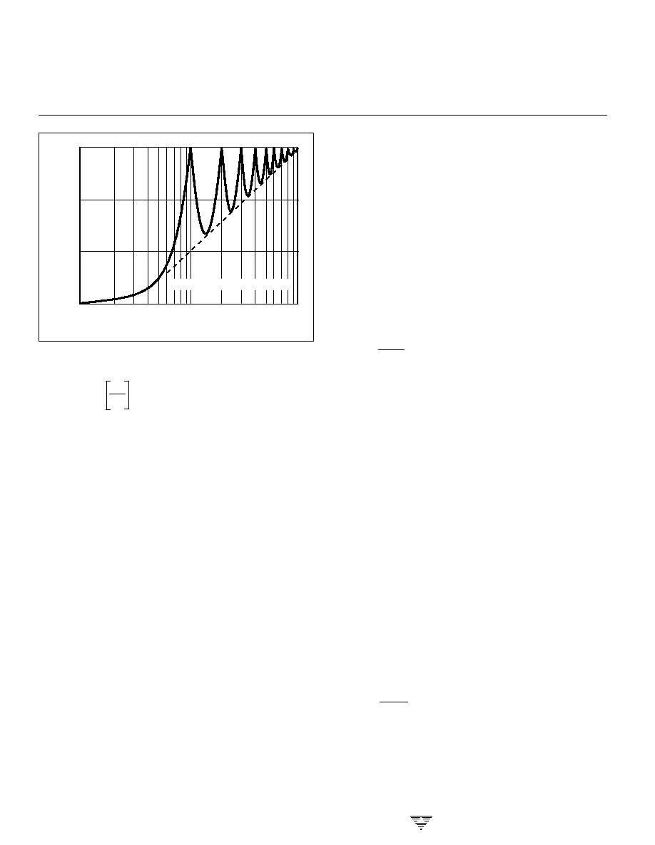
NORMAL MODE REJECTION (dB)
0.1/t
1/t
10/t
INPUT FREQUENCY
t = MEASUREMENT PERIOD
For a constant V
IN
:
V
IN
= V
R
.
t
RI
t
SI
The dual-slope converter accuracy is unrelated to the
integrating resistor and capacitor values, as long as they are
stable during a measurement cycle. Noise immunity is an
inherent benefit. Noise spikes are integrated, or averaged,
to zero during integration periods. Integrating ADCs are
immune to the large conversion errors that plague succes-
sive approximation converters in high-noise environments.
Interfering signals with frequency components at multiples
of the averaging period will be attenuated. Integrating ADCs
commonly operate with the signal integration period set to a
multiple of the 50 Hz/60 Hz power line period.
ANALOG SECTION
In addition to the basic integrate and deintegrate dual-
slope cycles discussed above, the TC7126A design incor-
porates an auto-zero cycle. This cycle removes buffer
amplifier, integrator, and comparator offset voltage error
terms from the conversion. A true digital zero reading results
without external adjusting potentiometers. A complete con-
version consists of three phases:
(1) Auto-zero phase
(2) Signal integrate phase
(3) Reference integrate phase
Auto-Zero Phase
During the auto-zero phase, the differential input signal
is disconnected from the circuit by opening internal analog
gates. The internal nodes are shorted to analog common
(ground) to establish a zero input condition. Additional
Figure 2. Normal-Mode Rejection of Dual-Slope Converter

3-223
TELCOM SEMICONDUCTOR, INC.
7
6
5
4
3
1
2
8
3-1/2 DIGIT
ANALOG-TO-DIGITAL CONVERTERS
TC7126
TC7126A
Figure 3. TC7126A Block Diagram
TC7126A
THOUSANDS
HUNDREDS
TENS
UNITS
4
39
OSC
V
TEST
1
TO SWITCH DRIVERS
FROM COMPARATOR OUTPUT
CLOCK
7 SEGMENT
DECODE
40
38
2
OSC
3
OSC
1
˜
CONTROL LOGIC
26
500
DATA LATCH
+
BUFF
C
REF
≠
R
INT
V
+
C
AZ
V
INT
28
29
27
33
36
34
10
µA
31
ZI & AZ
INT
AZ & DE (±)
32
INT
26
INTEGRATOR
TO
DIGITAL
SECTION
DE (+)
DE
(≠)
DE
(+)
DE (≠)
ANALOG
COMMON
C
REF
+
V
IN
+
V
IN
≠
V
C
INT
V
REF
+
V
REF
≠
ZI &
AZ
C
REF
+
35
+
≠
LCD SEGMENT DRIVERS
200
BP
f OSC
V
≠
V
TH
= 1V
V
≠
+
≠
INTERNAL DIGITAL GOUND
LOW
TEMPCO
V
REF
COMPARATOR
≠
AZ
ZI
V
+
≠ 2.8V
1
R
OSC
C
OSC
7 SEGMENT
DECODE
7 SEGMENT
DECODE
21
TYPICAL SEGMENT OUTPUT
INTERNAL DIGITAL GROUND
SEGMENT
OUTPUT
V
+
0.5 mA
2 mA
6.2V
LCD
+
≠

3-224
TELCOM SEMICONDUCTOR, INC.
3-1/2 DIGIT
ANALOG-TO-DIGITAL CONVERTERS
TC7126
TC7126A
The TC7126A is a drop-in replacement for the TC7126
and ICL7126 that offers a greatly improved internal refer-
ence temperature coefficient. No external component value
changes are required to upgrade existing designs.
COMPONENT VALUE SELECTION
Auto-Zero Capacitor (C
AZ
)
The C
AZ
size has some influence on system noise. A
0.33
µ
F capacitor is recommended for 200 mV full-scale
applications where 1 LSB is 100
µ
V. A 0.033
µ
F capacitor is
adequate for 2V full-scale applications. A Mylar-type dielec-
tric capacitor is adequate.
Reference Voltage Capacitor (C
REF
)
The reference voltage, used to ramp the integrator
output voltage back to zero during the reference integrate
phase, is stored on C
REF
. A 0.1
µ
F capacitor is acceptable
when V
REF
≠
is tied to analog common. If a large common-
mode voltage exists (V
REF
≠
analog common) and the
application requires a 200 mV full scale, increase C
REF
to
1
µ
F. Roll-over error will be held to less than 0.5 count. A
Mylar-type dielectric capacitor is adequate.
Integrating Capacitor (C
INT
)
C
INT
should be selected to maximize integrator output
voltage swing without causing output saturation. Due to
the TC7126A's superior analog common temperature co-
efficient specification, analog common will normally sup-
ply the differential voltage reference. For this case, a
±
2V
full-scale integrator output swing is satisfactory. For 3
readings per second (f
OSC
= 48 kHz), a 0.047
µ
F value is
suggested. For 1 reading per second, 0.15
µ
F is recom-
mended. If a different oscillator frequency is used, C
INT
must be changed in inverse proportion to maintain the
nominal
±
2V integrator swing.
An exact expression for C
INT
is:
When a segment driver is in-phase with the backplane
signal, the segment is OFF. An out-of-phase segment drive
signal causes the segment to be ON, or visible. This AC drive
configuration results in negligible DC voltage across each
LCD segment, ensuring long LCD life. The polarity segment
driver is ON for negative analog inputs. If V
IN
+
and V
IN
≠
are
reversed, this indicator would reverse.
On the TC7126A, when the TEST pin is pulled to V
+
, all
segments are turned ON. The display reads ≠1888. During
this mode, LCD segments have a constant DC voltage
impressed. DO NOT LEAVE THE DISPLAY IN THIS MODE
FOR MORE THAN SEVERAL MINUTES; LCDS MAY BE
DESTROYED IF OPERATED WITH DC LEVELS FOR
EXTENDED PERIODS.
The display font and segment drive assignment are
shown in Figure 4.
System Timing
The oscillator frequency is 4 prior to clocking the
internal decade counters. The three-phase measurement
cycle takes a total of 4000 counts (16,000 clock pulses).
The 4000-count cycle is independent of input signal magni-
tude.
Each phase of the measurement cycle has the following
length:
(1) Auto-zero phase: 1000 to 3000 counts
(4000 to 12,000 clock pulses)
For signals less than full scale, the auto-zero phase
is assigned the unused reference integrate time
period.
(2) Signal integrate:
1000 counts
(4000 clock pulses)
This time period is fixed. The integration period is:
t
SI
= 4000
,
where f
OSC
is the externally-set clock frequency.
(3) Reference integrate: 0 to 2000 counts
(0 to 8000 clock pulses)
where: f
OSC
= Clock frequency at pin 38
V
FS
= Full-scale input voltage
R
INT
= Integrating resistor
V
INT
= Desired full-scale integrator output swing.
At 3 readings per second, a 750
resistor should be
placed in series with C
INT
. This increases accuracy by
compensating for comparator delay. C
INT
must have low
dielectric absorption to minimize roll-over error. A polypro-
pylene capacitor is recommended.
1
f
OSC
DISPLAY FONT
1000's
100's
10's
1's
Figure 4. Display Font and Segment Assignment
C
INT
=
,
(
(
)
)
(4000)
V
INT
1
f
OSC
V
FS
R
INT
3-225
TELCOM SEMICONDUCTOR, INC.
7
6
5
4
3
1
2
8
3-1/2 DIGIT
ANALOG-TO-DIGITAL CONVERTERS
TC7126
TC7126A
In some applications, a scale factor other than unity may
exist between a transducer output voltage and the required
digital reading. Assume, for example, a pressure transducer
output for 2000 lb/in.
2
is 400 mV. Rather than dividing the
Required Full-Scale Voltage*
V
REF
200 mV
100 mV
2V
1V
*V
FS
= 2 V
REF
.
input voltage by two, the reference voltage should be set to
200 mV. This permits the transducer input to be used
directly.
The differential reference can also be used where a
digital zero reading is required when V
IN
is not equal to zero.
This is common in temperature-measuring instrumentation.
A compensating offset voltage can be applied between
analog common and V
IN
≠
. The transducer output is con-
nected between V
IN
+
and analog common.
DEVICE PIN FUNCTIONAL DESCRIPTION
(Pin Numbers Refer to 40-Pin DIP)
Differential Signal Inputs
V
IN
+
(Pin 31), V
IN
≠
(Pin 30)
The TC7126A is designed with true differential inputs
and accepts input signals within the input stage common-
mode voltage range (V
CM
). Typical range is V
+
≠1V to V
≠
+1V. Common-mode voltages are removed from the system
when the TC7126A operates from a battery or floating power
source (isolated from measured system), and V
IN
≠
is con-
nected to analog common (V
COM
). (See Figure 5.)
In systems where common-mode voltages exist, the
TC7126A's 86 dB common-mode rejection ratio minimizes
error. Common-mode voltages do, however, affect the inte-
grator output level. A worst-case condition exists if a large
positive V
CM
exists in conjunction with a full-scale negative
differential signal. The negative signal drives the integrator
output positive along with V
CM
(see Figure 6.) For such
applications, the integrator output swing can be reduced
below the recommended 2V full-scale swing. The integrator
output will swing within 0.3V of V
+
or V
≠
without increased
linearity error.
Differential Reference
V
REF
+
(Pin 36), V
REF
≠
(Pin 35)
The reference voltage can be generated anywhere
within the V
+
to V
≠
power supply range.
To prevent roll-over type errors being induced by large
common-mode voltages, C
REF
should be large compared to
stray node capacitance.
The TC7126A offers a significantly improved analog
common temperature coefficient. This potential provides a
very stable voltage, suitable for use as a voltage reference.
The temperature coefficient of analog common is typically
35 ppm/
∞
C for the TC7126A and 80 ppm/
∞
C for the TC7126.
ANALOG COMMON (Pin 32)
The analog common pin is set at a voltage potential
approximately 3V below V
+
. The potential is guaranteed to
be between 2.7V and 3.35V below V
+
. Analog common is
tied internally to an N-channel FET capable of sinking
Integrating Resistor (R
INT
)
The input buffer amplifier and integrator are designed
with Class A output stages. The output stage idling current
is 6
µ
A. The integrator and buffer can supply 1
µ
A drive
current with negligible linearity errors. R
INT
is chosen to
remain in the output stage linear drive region, but not so
large that PC board leakage currents induce errors. For a
200 mV full scale, R
INT
is 180 k
. A 2V full scale requires
1.8 M
.
Oscillator Components
C
OSC
should be 50 pF; R
OSC
is selected from the
equation:
f
OSC
=
.
For a 48 kHz clock (3 conversions per second), R = 180 k
.
Note that f
OSC
is 4 to generate the TC7126A's inter-
nal clock. The backplane drive signal is derived by dividing
f
OSC
by 800.
To achieve maximum rejection of 60 Hz noise pickup,
the signal integrate period should be a multiple of 60 Hz.
Oscillator frequencies of 240 kHz, 120 kHz, 80 kHz, 60 kHz,
40 kHz, etc. should be selected. For 50 Hz rejection,
oscillator frequencies of 200 kHz, 100 kHz, 66-2/3 kHz, 50
kHz, 40 kHz, etc. would be suitable. Note that 40 kHz (2.5
readings per second) will reject both 50 Hz and 60 Hz.
Reference Voltage Selection
A full-scale reading (2000 counts) requires the input
signal be twice the reference voltage.
Component Nominal Full-Scale Voltage
Value
200 mV
2V
C
AZ
0.33
µ
F
0.033
µ
F
R
INT
180 k
1.8 M
C
INT
0.047
µ
F
0.047
µ
F
NOTE:
f
OSC
= 48 kHz (3 readings per sec).
0.45
RC

3-226
TELCOM SEMICONDUCTOR, INC.
3-1/2 DIGIT
ANALOG-TO-DIGITAL CONVERTERS
TC7126
TC7126A
Figure 5. Common-Mode Voltage Removed in Battery Operation With V
IN
= Analog Common
100
µ
A. This FET will hold the common line at 3V should an
external load attempt to pull the common line toward V
+
.
Analog common source current is limited to 1
µ
A. Therefore,
analog common is easily pulled to a more negative voltage
(i.e., below V
+
≠ 3V).
The TC7126A connects the internal V
+
IN
and V
≠
IN
in-
puts to analog common during the auto-zero phase. During
the reference-integrate phase, V
≠
IN
is connected to analog
common. If V
+
IN
is not externally connected to analog com-
mon, a common-mode voltage exists, but is rejected by the
converter's 86 dB common-mode rejection ratio. In battery
operation, analog common and V
≠
IN
are usually connected,
removing common-mode voltage concerns. In systems where
V
≠
IN
is connected to power supply ground or to a given
voltage, analog common should be connected to V
≠
IN
.
The analog common pin serves to set the analog sec-
tion reference, or common point. The TC7126A is specifi-
cally designed to operate from a battery or in any measure-
ment system where input signals are not referenced (float)
with respect to the TC7126A's power source. The analog
common potential of V
+
≠3V gives a 7V end of battery life
voltage. The common potential has a 0.001%/% voltage
coefficient and a 15
output impedance.
With sufficiently high total supply voltage (V
+
≠V
≠
>7V),
analog common is a very stable potential with excellent
temperature stability (typically 35 ppm/
∞
c). This potential
can be used to generate the TC7126A's reference voltage.
An external voltage reference will be unnecessary in most
cases because of the 35 ppm/
∞
C temperature coefficient.
See "TC7126A Internal Voltage Reference" discussion.
TEST (Pin 37)
The TEST pin potential is 5V less than V
+
. TEST may be
used as the negative power supply connection for external
CMOS logic. The TEST pin is tied to the internally-generated
negative logic supply through a 500
resistor. The TEST pin
load should not be more than 1 mA. See "Digital Section" for
additional information on using TEST as a negative digital
logic supply.
If TEST is pulled HIGH (to V
+
),
all segments plus the
minus sign will be activated. DO NOT OPERATE IN THIS
MODE FOR MORE THAN SEVERAL MINUTES. With
TEST= V
+
, the LCD segments are impressed with a DC
voltage which will destroy the LCD.
TC7126A Internal Voltage Reference
The TC7126A's analog common voltage temperature
stability has been significantly improved (Figure 7). The "A"
version of the industry-standard TC7126 device allows
users to upgrade old systems and design new systems
without external voltage references. External R and C val-
ues do not need to be changed. Figure 10 shows analog
common supplying the necessary voltage reference for the
TC7126A.
VBUFF
CAZ VINT
BP
POL
SEGMENT
DRIVE
OSC1
OSC3
OSC2
V
≠
V
+
VREF
+
VREF
≠
ANALOG
COMMON
V
≠
V
+
V
≠
V
+
GND
GND
MEASURED
SYSTEM
POWER
SOURCE
9V
LCD
TC7126A
+
V
≠
V
+
IN
IN
Figure 6. Common-Mode Voltage Reduces Available Integrator
Swing (V
COM
V
IN
)
R
I
+
≠
V
IN
V
C
I
INTEGRATOR
V
I
=
[
[
V
CM
V
IN
≠
INPUT
BUFFER
C
I
=
=
R
I
Integration capacitor
Integration resistor
4000
f
Integration time
T
I
=
=
Where:
V
I
CM
OSC
≠
+
≠
+
TI
RI CI
3-227
TELCOM SEMICONDUCTOR, INC.
7
6
5
4
3
1
2
8
3-1/2 DIGIT
ANALOG-TO-DIGITAL CONVERTERS
TC7126
TC7126A
TYPICAL
GUARANTEED
MAXIMUM
TYPICAL
TYPICAL
200
180
160
140
120
100
80
60
40
20
0
ANALOG COMMON
TEMPERAT
URE COEFFICIENT (ppm/∞C)
TC7126A
ICL7136
NO
MAXIMUM
SPECIFIED
NO
MAXIMUM
SPECIFIED
ICL7126
Figure 8. TC7126A Internal Voltage Reference Connection
Figure 7. Analog Common Temperature Coefficient
APPLICATIONS INFORMATION
Liquid Crystal Display Sources
Several manufacturers supply standard LCDs to inter-
face with the TC7126A 3-1/2 digit analog-to-digital con-
verter.
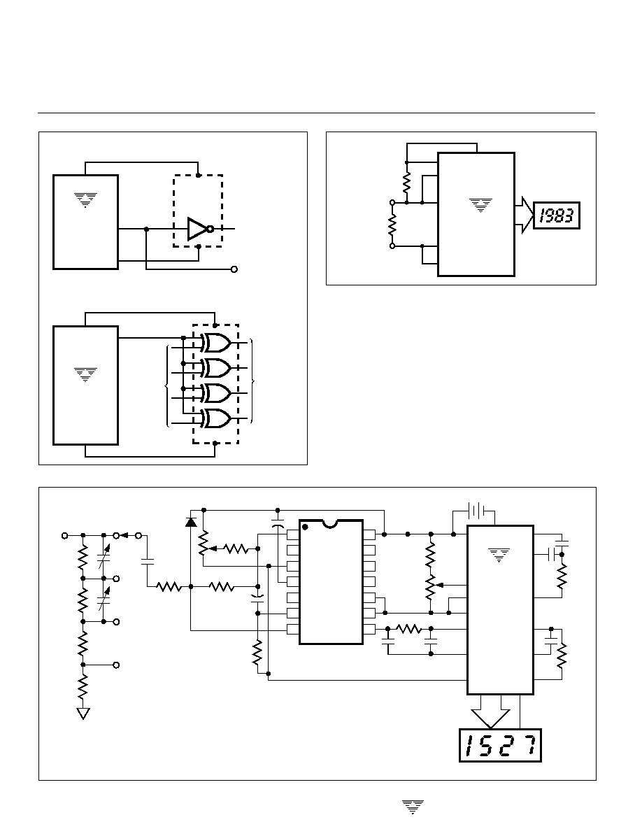
Decimal Point and Annunciator Drive
The TEST pin is connected to the internally-generated
digital logic supply ground through a 500
resistor. The
TEST pin may be used as the negative supply for external
CMOS gate segment drivers. LCD annunciators for decimal
points, low battery indication, or function indication may be
added without adding an additional supply. No more than 1
mA should be supplied by the TEST pin: its potential is
approximately 5V below V
+
.
Flat Package
The TC7126A is available in an epoxy 64-pin formed-
lead flat package. A test socket for the TC7126ACBQ device
is available:
Part No.
IC 51-42
Manufacturer: Yamaichi
Distribution:
Nepenthe Distribution
2471 East Bayshore
Suite 520
Palo Alto, CA 94043
(415) 856-9332
Ratiometric Resistance Measurements
The TC7126A's true differential input and differential
reference make ratiometric readings possible. In ratiometric
operation, an unknown resistance is measured with respect
to a known standard resistance. No accurately-defined
reference voltage is needed.
The unknown resistance is put in series with a known
standard and a current passed through the pair. The voltage
developed across the unknown is applied to the input and
the voltage across the known resistor applied to the refer-
ence input. If the unknown equals the standard, the display
will read 1000. The displayed reading can be determined
from the following expression:
Displayed reading =
1000.
The display will overrange for R
UNKNOWN
2
R
STANDARD
.
R
UNKNOWN
R
STANDARD
V
≠
ANALOG
COMMON
TC7126A
VREF
+
32
35
36
26
240 k
10 k
VREF
≠
VREF
1
+
9V
SET VREF = 1/2 VFULL SCALE
V
+
Representative
Manufacturer
Address/Phone
Part Numbers
*
Crystaloid
5282 Hudson Dr.,
C5335, H5535,
Electronics
Hudson, OH 44236
T5135, SX440
216-655-2429
AND
720 Palomar Avenue
FE 0801,
Sunnyvale, CA 94086
FE 0203
408-523-8200
VGI, Inc.
1800 Vernon St., Ste. 2
I1048, I1126
Roseville, CA 95678
916-783-7878
Hamlin, Inc.
612 E. Lake St.,
3902, 3933, 3903
Lake Mills, WI 53551
414-648-2361
*
NOTE: Contact LCD manufacturer for full product listing/specifications.
3-228
TELCOM SEMICONDUCTOR, INC.
3-1/2 DIGIT
ANALOG-TO-DIGITAL CONVERTERS
TC7126
TC7126A
8
14
7
13
12
11
10
9
1
2
3
4
5
6
TC7126A
9V
+
VIN
9 M
900 k
90 k
10 k
2V
20V
200V
200 mV
1N4148
10 M
1 M
0.02
µF
1 M
10%
47 k
1W
10%
20 k
10%
6.8 µF
1 µF
COM
C1 = 3 pF TO 10 pF, VARIABLE
C2 = 132 pF, VARIABLE
+
+
AD636
2.2
µF
0.01
µF
10 k
240 k
SEGMENT
DRIVE
LCD
39
40
28
27
38
29
26
1
35
32
31
30
26
36
BP
V
+
V
≠
V
+
REF
V
≠
REF
ANALOG
COMMON
V
+
IN
V
+
OUT
V
≠
C1
C2
Figure 9. Decimal Point and Annunciator Drives
Figure 11. 3-1/2 Digit True RMS AC DMM
V
REF
+
V
REF
≠
V
IN
+
V
IN
≠
ANALOG
COMMON
TC7126A
LCD
R
STANDARD
R
UNKNOWN
V
+
TC7126A
DECIMAL
POINT
SELECT
V
+
V
+
TEST
GND
4030
TO LCD
DECIMAL
POINTS
BP
TC7126A
BP
TEST
37
21
V+
V+
GND
TO LCD
DECIMAL
POINT
TO
BACKPLANE
4049
Multiple Decimal Point or
Annunciator Driver
Simple Inverter for Fixed Decimal Point
or Display Annunciator
Figure 10. Low Parts Count Ratiometric Resistance Measurement
3-229
TELCOM SEMICONDUCTOR, INC.
7
6
5
4
3
1
2
8
3-1/2 DIGIT
ANALOG-TO-DIGITAL CONVERTERS
TC7126
TC7126A
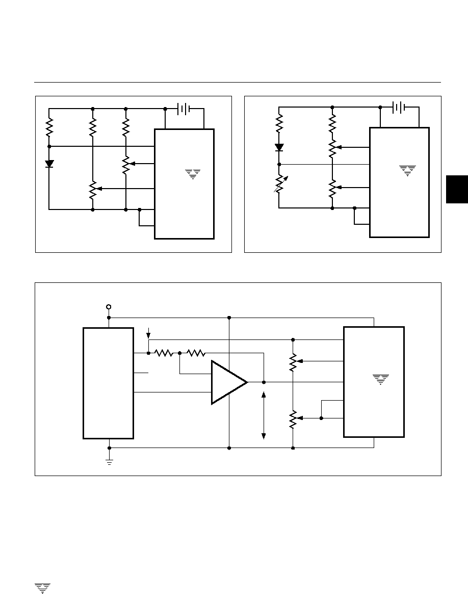
Figure 12. Temperature Sensor
Figure 13. Positive Temperature Coefficient Resistor
Temperature Sensor
Figure 14. Integrated Circuit Temperature Sensor
TC7126A
≠
+
9V
V
+
2
6
8
3
NC
GND
4
TEMPERATURE
DEPENDENT OUTPUT
3
5
4
1
2
REF02
ADJ
VOUT
TEMP
CONSTANT 5V
51 k
1/2
LM358
VOUT =
1.86V @
+25∞C
R1
50 k
50 k
R2
COMMON
VIN
≠
VIN
+
VREF
≠
VREF
+
V ≠
V
+
51 k
R4
R5
TC7126A
V
+
V
≠
VIN
≠
VIN
+
VREF
+
VREF
≠
COMMON
5.6 k
160 k
R2
20 k
1N4148
9V
R1
20 k
+
R3
0.7%/∞C
PTC
TC7126A
V
+
V
≠
VIN
≠
VIN
+
VREF
+
VREF
≠
COMMON
50 k
R2
160 k
300 k
300 k
R1
50 k
1N4148
SENSOR
9V
+