 | –≠–ª–µ–∫—Ç—Ä–æ–Ω–Ω—ã–π –∫–æ–º–ø–æ–Ω–µ–Ω—Ç: TC7211AM | –°–∫–∞—á–∞—Ç—å:  PDF PDF  ZIP ZIP |
Document Outline
- Return to Contents
- List of Figures
- 1. BUS Interface Timing Diagram
- 2. LCD Display Waveforms
- 3. TC7211AM Driving an 8-Digit LCD Display
- 4. Segment Assignment
- List of Tables
- 1. Binary Codes Versus Character Displayed
- Features
- Pin Configurations
- General Description
- Ordering Information
- Functional Block Diagram
- Absolute Maximum Ratings*
- Typical Characteristics
- Timing Diagrams
- Input Definitions
- Output Definitions
- Digit Assignment
- Typical Characteristics
- Basic Operation
- Input Configuration and Output Codes
- Special Order Decoder Option
6-7
TELCOM SEMICONDUCTOR, INC.
7
6
5
4
3
1
2
8
TC7211AM
BUS COMPATIBLE 4-DIGIT CMOS DECODER/DRIVER
FEATURES
s
4-Digit Non-Multiplexed 7-Segment LCD Outputs
With Backplane Driver
s
Input and Digit Select Data Latches
s
RC Oscillator On-Chip Generates Backplane
Drive Signal
s
Eliminates DC Bias Which Degrades LCD Life
s
Backplane Input/Output Pin Permits
Synchronization of Cascaded Slave Device to
a Master Backplane Signal
s
Binary and BCD Inputs Decoded to Code B
(0 to 9, --, E, H, L, P, Blank)
s
Pin Compatible and Functionally Equivalent to
ICM7211AM
GENERAL DESCRIPTION
The TC7211AM (LCD Decoder/driver) is a CMOS di-
rect drive, 4-digit, 7-segment display decoder and driver.
The TC7211AM drives conventional LCDs. An RC os-
cillator, divider chain, backplane driver, and 28-segment
outputs are provided on a single CMOS chip. The segment
drivers supply square waves of the same frequency as the
backplane, but in-phase for an OFF segment and out-of-
phase for an ON segment. The net DC voltage applied
between driver segment and backplane is near zero maxi-
mizing display lifetime.
The four bit binary input is decoded into the seven
segment alphanumeric code known as "Code B". The "Code
B" output format results in a 0 to 9,--, E, H, L, P or blank
display. True BCD or binary inputs will be correctly de-
coded to the seven segment display format.
ORDERING INFORMATION
Driver
Input
Output
Part No.
Type
Package Code
Config.
Data and
TC7211AMIPL
LCD
40-Pin
Code B
Digit Select
Plastic DIP
Latches
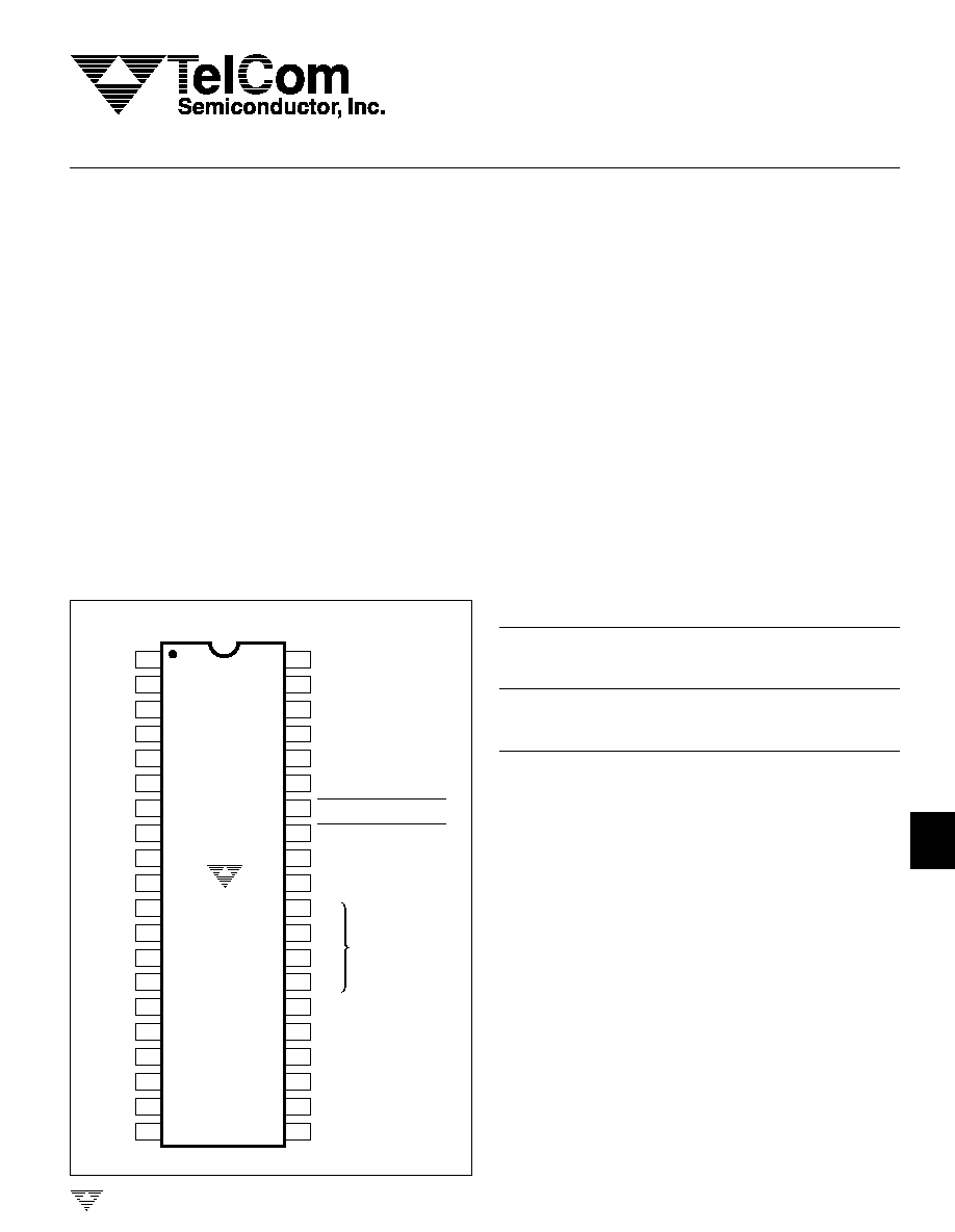
PIN CONFIGURATIONS
TC7211AM-4 11/14/96
TC7211AM (LCD)
1
2
3
4
D1
5
6
7
8
9
10
11
12
A1
OSCILLATOR
B2
V
+
E1
D2
13
14
15
16
17
18
19
20
40
39
38
37
36
35
34
33
32
31
30
29
28
27
26
25
24
23
22
21
G1
F1
BP
A2
B2
C2
E2
G2
F2
A3
B3
C3
D3
E3
G3
F3
C1
B1
GND
B3
B1
B0
F4
G4
E4
D4
C4
B4
A4
DATA
INPUTS
CHIP SELECT 2 (CS2)
CHIP SELECT 1 (CS1)
DIGIT SELECT 2 (DS2
DIGIT SELECT 1 (DS1

6-8
TELCOM SEMICONDUCTOR, INC.
BUS COMPATIBLE, 4-DIGIT
CMOS DECODER/DRIVER
TC7211AM
FUNCTIONAL BLOCK DIAGRAM
D4
SEGMENT
OUTPUTS
D3
SEGMENT
OUTPUTS
D2
SEGMENT
OUTPUTS
D1
SEGMENT
OUTPUTS
ENABLE
DETECTOR
OSCILLATOR
(16 kHz
FREE-
RUNNING)
˜
128
BACK≠
PLANE
DRIVER
ENABLE
BACKPLANE
(INPUT/OUTPUT)
V+
GND
DATA
INPUTS
DIGIT
SELECT
INPUTS
TC7211AM
PROGRAMMABLE
4-TO-7 DECODER
PROGRAMMABLE
4-TO-7 DECODER
PROGRAMMABLE
4-TO-7 DECODER
PROGRAMMABLE
4-TO-7 DECODER
7 WIDE
DRIVER
7 WIDE
DRIVER
7 WIDE
DRIVER
7 WIDE
DRIVER
7 WIDE
LATCH ENABLE
7 WIDE
LATCH ENABLE
7 WIDE
LATCH ENABLE
7 WIDE
LATCH ENABLE
OSCILLATOR
INPUT
1
35
B0
27
28
29
30
4-BIT
LATCH
B1
B2
B3
2-BIT
LATCH
2-TO-4
DECODER
DS1
DS2
31
32
33
34
CS1
CS2
ONE SHOT
ENABLE
ENABLE
ENABLE
36
g
a

6-9
TELCOM SEMICONDUCTOR, INC.
7
6
5
4
3
1
2
8
Symbol
Parameter
Test Conditions
Min
Typ
Max
Unit
V
SUP
Operating Voltage Range
3
5
6
V
I
OP
Operating Current
Display Blank
--
10
50
µ
A
I
OSCI
Oscillator Input Current
Pin 36
--
±
2
±
10
µ
A
t
RFS
Segment Rise/Fall Time
C
L
= 200 pF
--
0.5
--
µ
sec
t
RFB
Backplane Rise/Fall Time
C
L
= 5000 pF
--
1.5
--
µ
sec
f
OSC
Oscillator Frequency
Pin 36 Floating
--
16
--
kHz
f
BP
Backplane Frequency
Pin 36 Floating
--
125
--
Hz
Input Characteristics
V
IH
Logic "1" High Input Voltage
3
--
--
V
V
IL
Logic "0" Low Input Voltage
--
--
1
V
I
ILK
Input Leakage Current
Pins 27≠34
--
±
0.01
±
1
µ
A
C
IN
Input Capacitance
Pins 27≠34
--
5
--
pF
I
BPLK
BP Input Current
Measured at Pin 5 With
--
±
0.01
±
1
µ
A
Leakage
Pin 36 at GND
C
BPI
BP Input Capacitance
All Devices
--
200
--
pF
AC Characteristics
Symbol
Parameter
Test Conditions
t
CSA
Chip Select Active Pulse Width
(Note 1)
200
--
--
nsec
t
DS
Data Setup Time
100
--
--
nsec
t
DH
Data Hold Time
10
0
--
nsec
t
ICS
Inter-Chip Select Time
2
--
--
µ
sec
NOTE: 1. Other chip select (CS) is either held at logic zero or both CS1 and CS2 driven together.
*Stresses above those listed under "Absolute Maximum Ratings" may
cause permanent damage to the device. These are stress ratings only, and
functional operation of the device at these or any other conditions above
those indicated in the operational sections of the specifications is not
implied. Exposure to absolute maximum rating conditions for extended
periods may affect device reliability.
NOTES: 1. This limit refers to that of the package and will not be realized
during normal operation.
2. Due to the SCR structure inherent in the CMOS process,
connecting any terminal to voltages greater than V
+
or less
than GND may cause destructive latch-up. For this reason, it
is recommended that inputs from external sources not oper-
ating on the same power supply not be applied to the device
before its supply is established, and, in multiple supply
systems, the supply to the TC7211AM be turned on first.
ABSOLUTE MAXIMUM RATINGS*
Supply Voltage ........................................................ +6.5V
Input Voltage, Any Terminal
(Note 2) .................................... V
+
+0.3V, GND ≠0.3V
Power Dissipation T
A
70
∞
C (Note 1) ................... 1.23W
Operating Temperature Range ................ ≠20
∞
C to +85
∞
C
Storage Temperature Range ................. ≠65
∞
C to +150
∞
C
Lead Temperature (Soldering, 10 sec) ................. +300
∞
C
TYPICAL CHARACTERISTICS:
All parameters measured with V+ = 5V, T
A
= 25
∞
C
BUS COMPATIBLE, 4-DIGIT
CMOS DECODER/DRIVER
TC7211AM

6-10
TELCOM SEMICONDUCTOR, INC.
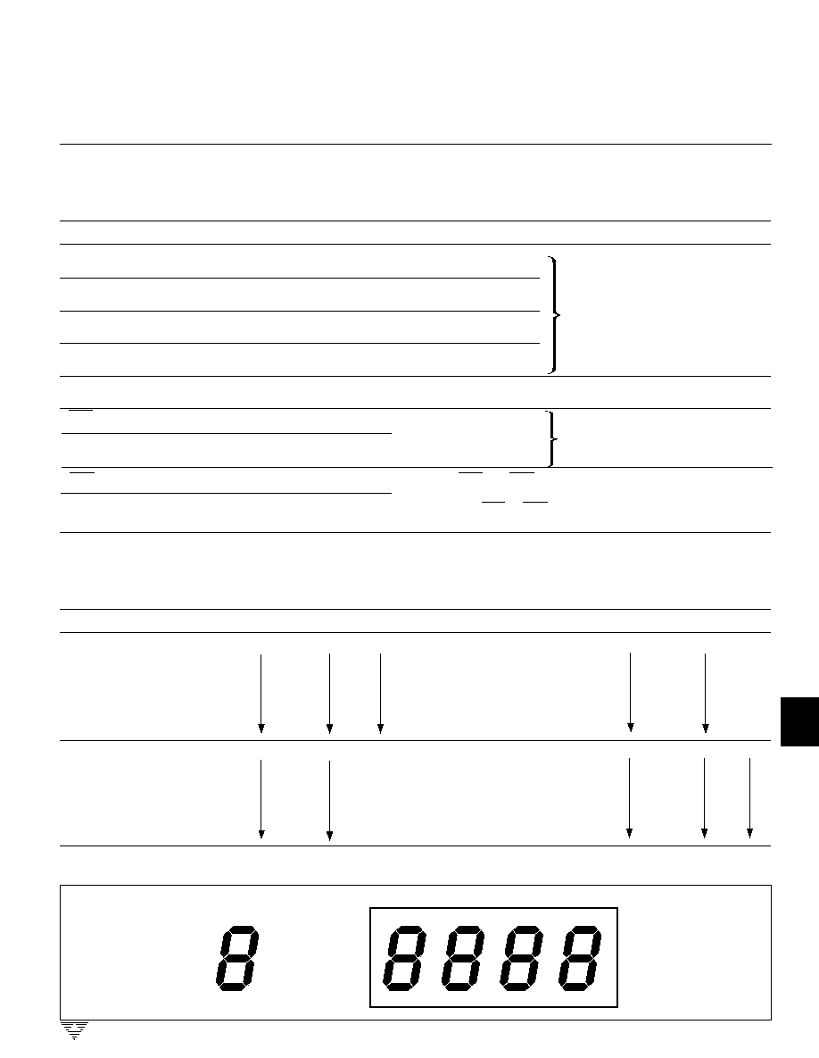
TIMING DIAGRAMS
Figure 2: LCD Display Waveforms
128 CYCLES
64
CYCLES
64
CYCLES
OSCILLATOR
FREQUENCY
BACKPLANE
INPUT/OUTPUT
OFF SEGMENTS
ON SEGMENTS
tCSA
tICS
tDS
tDH
,
,
,
,
,
CS1
(CS2)
CS2
(CS1)
DATA AND
DIGIT
SELECT
CODE
DON'T CARE
Figure 1: BUS Interface Timing Diagram
BUS COMPATIBLE, 4-DIGIT
CMOS DECODER/DRIVER
TC7211AM
6-11
TELCOM SEMICONDUCTOR, INC.
7
6
5
4
3
1
2
8
INPUT DEFINITIONS
In this table, V
+
and GND are considered to be normal operating input logic levels. For lowest power consumption, input
signals should swing over the full supply.
Input
Pin No.
Condition
Function
B0
27
V
+
= Logic "1"
GND = Logic "0"
Ones (Least Significant)
B1
28
V
+
= Logic "1"
GND = Logic "0"
Twos
B2
29
V
+
= Logic "1"
GND = Logic "0"
Fours
B3
30
V
+
= Logic "1"
GND = Logic "0"
Eights (Most Significant)
OSC
36
Floating or with
Oscillator input. Disables BP output devices, allowing segments to be
external capacitor GND
synchronized to an external signal input at the BP terminal (pin 5)
DS1
31
V
+
= Logical One
DS2, DS1 = 00 Selects D4
DS2, DS1 = 01 Selects D3
DS2
32
GND = Logical Zero
DS2, DS1 = 10 Selects D2
DS2, DS1 = 11 Selects D1
CS1
33
V
+
= Inactive
When both CS1 and CS2 are LOW, the data and digit select input
latches are open or enabled.
CS2
34
GND = Active
On the rising of CS1 or CS2, data is latched, decoded and stored in
the output drive latches.
BUS COMPATIBLE, 4-DIGIT
CMOS DECODER/DRIVER
TC7211AM
Digit Select Inputs
DIGIT ASSIGNMENT
OUTPUT DEFINITIONS
Output pins are defined by the alphabetical segment assignment and numerical digital assignment.
Output
Pin No.
Function
Output
Pin No.
Function
A1
37
A
Segment Drive
Digit 1
(LSD)
A3
13
A
Segment Drive
Digit 3
B1
38
B
B3
14
B
C1
39
C
C3
15
C
D1
40
D
D3
16
D
E1
2
E
E3
17
E
F1
4
F
F3
19
F
G1
3
G
G3
18
G
A2
6
A
Segment Drive
Digit 2
A4
20
A
Segment Drive
Digit 4
(MSD)
B2
7
B
B4
21
B
C2
8
C
C4
22
C
D2
9
D
D4
23
D
E2
10
E
E4
24
E
F2
12
F
F4
26
F
G2
11
G
G4
25
G
Data Input Bits
G
A
B
C
F
E
D
D4
D3
D2
D1

6-12
TELCOM SEMICONDUCTOR, INC.
BUS COMPATIBLE, 4-DIGIT
CMOS DECODER/DRIVER
TC7211AM
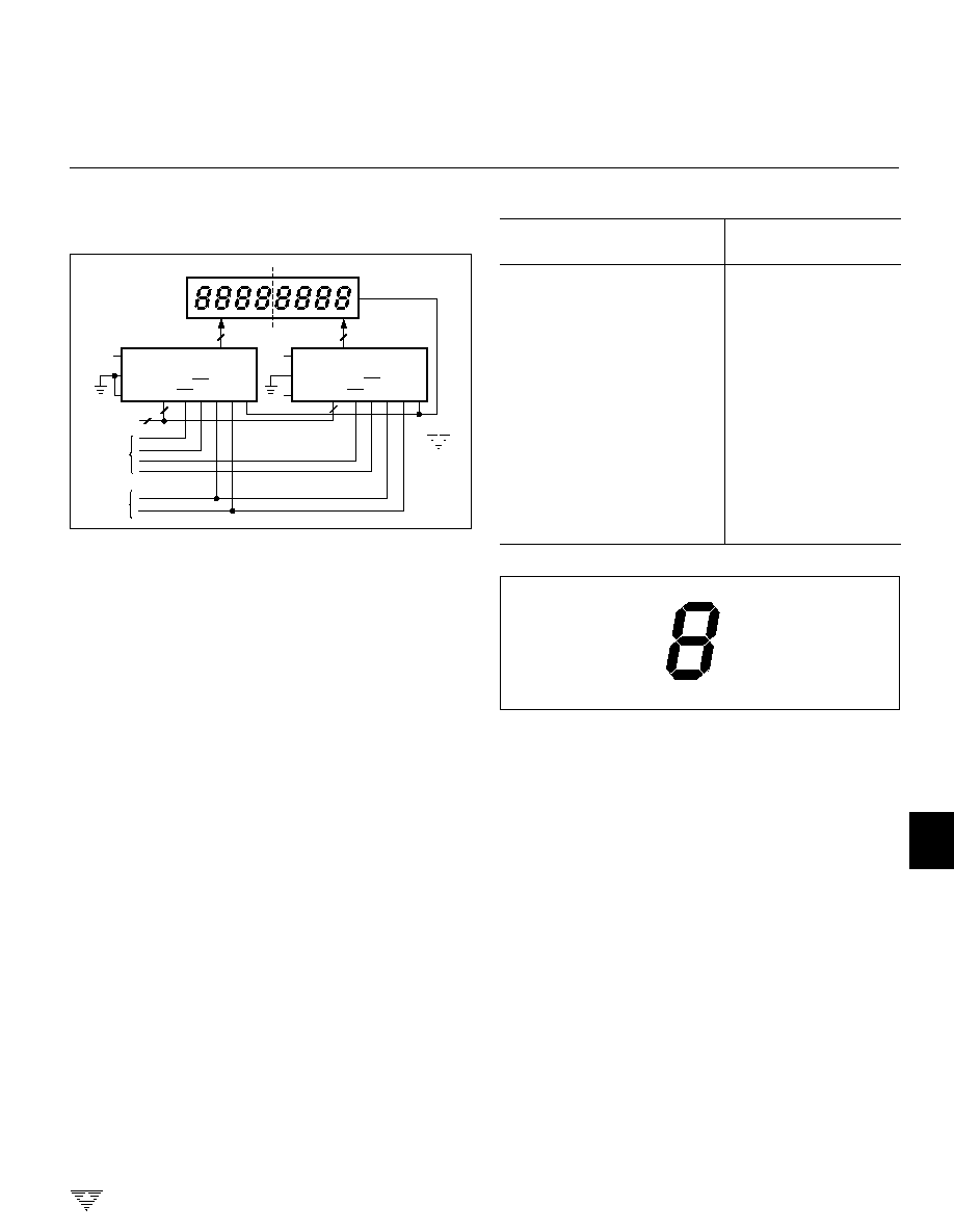
If more than four devices are slaved together, the
backplane signal should be derived externally and all
TC7211AM devices slaved to it. The external drive signal
must drive a high capacitive load with 1
µ
sec to 2
µ
sec rise
and fall times. The backplane frequency is normally 125
Hz. At lower display ambient temperatures, the frequency
may be reduced to compensate for display response time.
The on-chip RC oscillator free-runs at approximately
16 kHz. A divide-by 128 circuit provides the 125 Hz backplane
frequency. The oscillator frequency may be reduced by
connecting an external capacitor between the oscillator
terminal and V
+
. (See typical operating characteristics
curves.)
The free-running oscillator may be overridden (if de-
sired) by an external clock. The backplane driver, however,
must not be disabled during the external clock's negative or
lOW portion, as this will result in a DC drive component
being applied to the LCD, limiting the LCD's life. To
prevent backplane driver disabling, the oscillator input
should be driven from the positive supply to no less than
one-fifth the supply voltage above ground. A backplane
disable signal will not be sensed if the driving signal remains
above ground by one-fifth the supply voltage. An alternate
method for externally driving the oscillator permits the
oscillator input to swing the full supply voltage range. The
oscillator input signal duty cycle is skewed so the LOW
BASIC OPERATION
The TC7211AM drives 4-digit, 7-segment LCDs. This
device contains 28 individual segment drivers, a backplane
driver, a self-contained oscillator, and a divider chain to
generate the backplane signal.
The 28 CMOS segment drivers and backplane driver
contain ratioed N- and P-channel transistors for identical ON
resistance. The equal resistances eliminate the DC output
driver component resulting from unequal rise and fall times.
This ensures maximum LCD life.
The backplane output driver can be disabled by ground-
ing the OSCILLATOR input (pin 36). The 28 output segment
drivers can therefore be synchronized directly to an input
signal at the backplane (BP) terminal (pin 5). Several slave
devices may be cascaded to the backplane output of a
master device. The backplane signal may also be derived
from an external source. These features permit interfacing to
single backplane LCDs with characters in multiples of four.
Each slave's backplane input represents a 200pF
capacitive load to the master backplane driver (comparable
to one additional segment). The number of slave devices
drivable by a master device is therefore set by the larger
display backplane capacitive load. The master backplane
output will drive the display backplane of 16 one-half-inch
characters with rise and fall times under 5
µ
sec. This
represents a system with three slave devices and a fourth
master device driving the backplane.
TYPICAL CHARACTERISTICS
30
25
20
15
10
5
1
2
3
4
5
6
7
Operating Supply Current
vs Supply Voltage
TA= ≠20
∞
C
TA= +70
∞
C
TA= +25
∞
C
V+ VOLTS
I OP
(
µ
A)
0
LCD DEVICES
DISPLAY BLANK
PIN 36 OPEN
180
150
120
90
60
30
0
Backplane Frequency
vs Supply Voltage
COSC = 0 pF
V+ VOLTS
BP (Hz)
1
2
3
4
5
6
7
COSC = 22 pF
COSC = 220 pF
(PIN 36 OPEN)
TA = +25
∞
C
6-13
TELCOM SEMICONDUCTOR, INC.
7
6
5
4
3
1
2
8
Binary Input
Character Displayed
B3
B2
B1
B0
(Code B)
0
0
0
0
0
0
0
0
1
1
0
0
1
0
2
0
0
1
1
3
0
1
0
0
4
0
1
0
1
5
0
1
1
0
6
0
1
1
1
7
1
0
0
0
8
1
0
0
1
9
1
0
1
0
--
1
0
1
1
E
1
1
0
0
H
1
1
0
1
L
1
1
1
0
P
1
1
1
1
Blank
portion duration is less than 1
µ
sec. The backplane disable
sensing circuit will not respond to such a short signal.
Input Configuration and Output Codes
The TC7211AM accepts a 4-bit, true binary (positive
level = logic "1") input at pin 27 (LSB) through pin 30 (MSB).
The binary input is decoded to the 7-segment output known
as Code B. The output display format is 0 to 9, --, E, H, L,
P and blank display (see Table 1). Segment assignments
are shown in Figure 4. The TC7211AM will correctly decode
binary and BCD true codes to a 7-segment output.
The TC7211AM is designed to interface with a data bus
and display data under microprocessor control. Four data
inputs (pins 27≠30) and two digit select input bits (pins 31
and 32) are written into input buffer latches. The rising edge
of either chip select causes data to be latched, decoded and
stored in the selected digit output data latch. The 2-bit digit
code selects the appropriate output digit latch. The 4-bit
display data word is decoded to the "Code B" 7-segment
output format.
For applications where bus compatibility is not required,
refer to the TC7211AM (LCD) 4-digit decoder driver data
sheet. This device is designed to accept multiplexed BCD/
binary input data for display under the control of four sepa-
rate digit select control signals.
Figure 3. TC7211AM Driving an 8-Digit LCD Display
in Master/Slave Configuration
Figure 4. Segment Assignment
Special Order Decoder Option
The TC7211AM is mask programmed to give the 16
combinations of 7-segment output codes. For large volume
orders (50K pieces minimum), custom decoder options are
available. Contact TelCom Semiconductor for details.
D8 D7 D6 D5 D4
D3 D2 D1
8-DIGIT
LCD
BACKPLANE
SLAVE
BCD/BINARY
DATA
BACKPLANE
MASTER
BACKPLANE
28
+5V
4
4
4
V+
GND
OSC
SEGMENTS
HIGH ORDER
B3≠
B0 CS1
BP
+5V
V+
GND
OSC
SEGMENTS
HIGH ORDER
B3≠
B0
BP
TC7211AM
28
DS1
CS2
DS2
CS1
DS1
CS2
DS2
CHIP
SELECT
DIGIT
SELECT
G
A
B
C
F
E
D
Table 1. Binary Codes Versus Character Displayed
BUS COMPATIBLE, 4-DIGIT
CMOS DECODER/DRIVER
TC7211AM