 | –≠–ª–µ–∫—Ç—Ä–æ–Ω–Ω—ã–π –∫–æ–º–ø–æ–Ω–µ–Ω—Ç: TC7650 | –°–∫–∞—á–∞—Ç—å:  PDF PDF  ZIP ZIP |
Document Outline
- Return to Contents
- List of Figures
- 1. TC7650 Contains a Nulling and Main Amplifier. Offset Correction Voltages Are Stored on Two External Capacitors.
- 2. Nulling Capacitor Connection
- 3. Internal Clamp Circuit
- 4. Noninverting Amplifier With Optional Clamp
- 5. Inverting Amplifier with Optional Clamp
- 6. Input Guard Connection
- Features
- Ordering Information
- Functional Block Diagram
- General Description
- Pin Configurations
- Absolute Maximum Ratings
- Electrical Characteristics
- Electrical Characteristics
- Theory of Operation
- Output Stage/Loading
- Intermodulation
- Nulling Capacitor Connection
- Clock Operation
- Output Clamp
- Latch-Up Avoidance
- Thermoelectric Potentials
- Pin Compatibility
- Input Guarding
- Component Selection
- Typical Characteristics

3-273
TELCOM SEMICONDUCTOR, INC.
7
6
5
4
3
1
2
8
CHOPPER-STABILIZED OPERATIONAL AMPLIFIER
TC7650
GENERAL DESCRIPTION
The TC7650 CMOS chopper-stabilized operational
amplifier practically removes offset voltage error terms
from system error calculations. The 5
µ
V maximum V
OS
specification, for example, represents a 15 times improve-
ment over the industry-standard OP07E. The 50nV/
∞
C off-
set drift specification is over 25 times lower than the OP07E.
The increased performance eliminates V
OS
trim proce-
dures, periodic potentiometer adjustment and the reliability
problems caused by damaged trimmers.
The TC7650 performance advantages are achieved
without the additional manufacturing complexity and cost
incurred with laser or "zener zap" V
OS
trim techniques.
The TC7650 nulling scheme corrects both DC V
OS
errors and V
OS
drift errors with temperature. A nulling
amplifier alternately corrects its own V
OS
errors and the main
amplifier V
OS
error. Offset nulling voltages are stored on two
user-supplied external capacitors. The capacitors connect
to the internal amplifier V
OS
null points. The main amplifier
input signal is never switched. Switching spikes are not
present at the TC7650 output.
The 14-pin dual-in-line package (DIP has an external
oscillator input to drive the nulling circuitry for optimum noise
performance. Both the 8 and 14-pin DIPs have an output
voltage clamp circuit to minimize overload recovery time.
PIN CONFIGURATIONS
FEATURES
s
Low Input Offset Voltage ......................... 0.7
µ
V Typ
s
Low Input Offset Voltage Drift ......... 0.05
µ
V/
∞
C Max
s
Low Input Bias Current ............................ 10pA Max
s
High Impedance Differential CMOS Inputs .... 10
12
s
High Open-Loop Voltage Gain ................ 120dB Min
s
Low Input Noise Voltage ............................ 2.0
µ
Vp-p
s
High Slew Rate .......................................... 2.5V/
µ
sec
s
Low-Power Operation ..................................... 20mW
s
Output Clamp Speeds Recovery Time
s
Compensated Internally for Stable Unity Gain
Operation
s
Direct Replacement for ICL7650
s
Available in 8-Pin Dip and 14-Pin Dip
FUNCTIONAL BLOCK DIAGRAM
ORDERING INFORMATION
Temperature
Max
Part No.
Package
Range
V
OS
TC7650CPA
8-Pin Plastic DIP
0
∞
C to +70
∞
C
5
µ
V
TC7650CPD
14-Pin Plastic DIP
0
∞
C to +70
∞
C
5
µ
V
TC7650
NULL
NULL
INPUTS
OUTPUT
CLAMP
OUTPUT
B
B
A
CEXT
CEXT
FOR 8-PIN DIP, CONNECT TO VSS.
NULL
AMPLIFIER
MAIN
AMPLIFIER
OUTPUT CLAMP
CIRCUIT
INTERMOD
COMPENSATION
OSCILLATOR
A
B
INT/EXT
EXT CLK IN
CLK OUT
14-PIN DIP ONLY
B
A
CRET
*
*
TC7650-5 9/11/96
1
2
3
4
5
6
7
14
13
12
11
10
9
8
C
NC
(GUARD)
8-Pin DIP
V
SS
V
SS
INT/EXT
EXT CLK
INPUT
INT CLK
OUTPUT
OUTPUT
OUTPUT
CLAMP
RETN
B
C
A
C
V
DD
TC7650CPD
1
2
3
4
8
7
6
5
C
OUTPUT
A
V
DD
TC7650CPA
INPUT
INPUT
C
B
(+)
(≠)
CLAMP
INPUT
(≠)
INPUT
(+)
NC
(GUARD)
14-Pin DIP
NC = NO INTERNAL CONNECTION

3-274
TELCOM SEMICONDUCTOR, INC.
TC7650
CHOPPER-STABILIZED
OPERATIONAL AMPLIFIER
ELECTRICAL CHARACTERISTICS:
V
DD
= +5V, V
SS
= ≠5V, C
A
= C
B
= 0.1
µ
F, T
A
= 25
∞
C, unless otherwise
indicated.
Symbol
Parameter
Test Conditions
Min
Typ
Max
Units
Input
V
OS
Input Offset Voltage
T
A
= +25
∞
C
--
±
0.7
±
5
--
Over Operating Temp Range
--
±
1.0
--
µ
V
V
OS
/
T
Input Offset Voltage
Operating Temperature Range
--
0.01
0.05
µ
V/
∞
C
Average Temperature
Coefficient
Offset Voltage vs. Time
--
100
--
nV/
month
I
BIAS
Input Bias Current
T
A
= +25
∞
C
--
1.5
10
pA
0
∞
C
T
A
+70
∞
C
--
35
150
pA
≠25
∞
C
T
A
+85
∞
C
--
100
400
pA
I
OS
Input Offset Current
--
0.5
--
pA
e
NP-P
Input Noise Voltage
R
S
= 100
, 0 to 10Hz
--
2
--
µ
V
P-P
I
N
Input Noise Current
f = 10 Hz
--
0.01
--
pA/
Hz
R
IN
Input Resistance
--
10
12
CMVR
Common-Mode
≠ 5
≠ 5.2
+1.6
V
Voltage Range
to +2
CMRR
Common-Mode
CMVR = ≠5V to +1.5V
120
130
--
dB
Rejection Ratio
Output
A
Large Signal Voltage
R
L
= 10k
120
130
--
dB
Gain
V
OUT
Output Voltage Swing (Note 2)
R
L
= 10k
±
4.7
±
4.85
--
V
R
L
= 100k
--
±
4.95
--
V
Clamp ON Current
R
L
= 100k
25
70
200
µ
A
(Note 1)
Clamp OFF Current
≠ 4V < V
OUT
<
+4V
--
1
--
pA
(Note 1)
Dynamic
B
W
Unity-Gain Bandwidth
Unity Gain (+1)
--
2.0
--
MHz
S
R
Slew Rate
C
L
= 50 pF, R
L
= 10k
--
2.5
--
V/
µ
sec
t
R
Rise Time
--
0.2
--
µ
sec
Overshoot
--
20
--
%
f
CH
Internal Chopping
Pins 12≠14 Open (DIP)
120
200
375
Hz
Frequency
Package Power Dissipation (T
A
70
∞
C)
8-Pin Plastic DIP ............................................. 730mW
14-Pin Plastic DIP ........................................... 800mW
*Static-sensitive device. Unused devices must be stored in conductive
material. Protect devices from static discharge and static fields. Stresses
above those listed under Absolute Maximum Ratings may cause perma-
nent damage to the device. These are stress ratings only and functional
operation of the device at these or any other conditions above those
indicated in the operational sections of the specifications is not implied.
Exposure to Absolute Maximum Rating Conditions for extended periods
may affect device reliability.
ABSOLUTE MAXIMUM RATINGS*
Total Supply Voltage (V
DD
to V
SS
) .............................. 18V
Input Voltage ........................ (V
DD
+ 0.3V) to (V
SS
≠ 0.3V)
Storage Temperature Range ................ ≠ 65
∞
C to +150
∞
C
Lead Temperature (Soldering, 10 sec) ................... 300
∞
C
Voltage on Oscillator Control Pins ................... V
DD
to V
SS
Output Short Circuit Duration ............................. Indefinite
Current Into Any Pin ................................................. 10mA
While Operating (Note 3) .................................. 100
µ
A
Operating Temperature Range
C Device ................................................ 0
∞
C to +70
∞
C
3-275
TELCOM SEMICONDUCTOR, INC.
7
6
5
4
3
1
2
8
ELECTRICAL CHARACTERISTICS:
V
DD
= +5V, V
SS
= ≠ 5V, C
A
= C
B
= 0.1
µ
F, T
A
= 25
∞
C, unless otherwise
specified.
Symbol
Parameter
Test Conditions
Min
Typ
Max
Units
Supply
V
DD
, V
SS
Operating Supply Range
4.5
--
16
V
I
S
Supply Current
No Load
--
2
3.5
mA
PSRR
Power Supply
V
S
=
±
3V to
±
8V
120
130
dB
Rejection Ratio
NOTES: 1. See "Output Clamp" discussion.
2. Output clamp not connected. See typical characteristics curves for output swing versus clamp current characteristics.
3. Limiting input current to 100
µ
A is recommended to avoid latch-up problems.
CHOPPER-STABILIZED
OPERATIONAL AMPLIFIER
TC7650
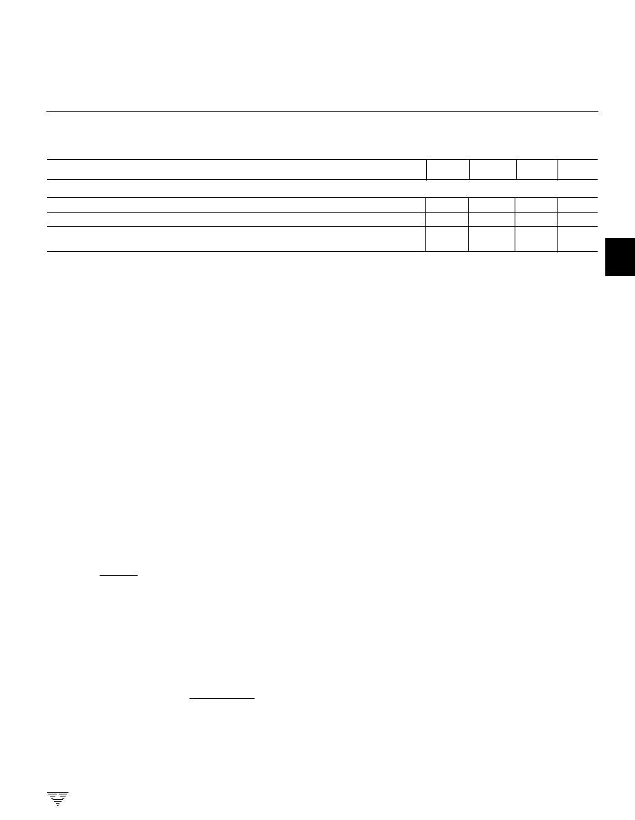
Theory of Operation
Figure 1 shows the major elements of the TC7650.
There are two amplifiers (the main amplifier and the nulling
amplifier), and both have offset-null capability. The main
amplifier is connected full-time from the input to the output.
The nulling amplifier, under the control of the chopping
frequency oscillator and clock circuit, alternately nulls itself
and the main amplifier. Two external capacitors provide the
required storage of the nulling potentials and the necessary
nulling-loop time constants. The nulling arrangement oper-
ates over the full common-mode and power-supply ranges,
and is also independent of the output level, thus giving
exceptionally high CMRR, PSRR, and A
VOL
.
Careful balancing of the input switches minimizes chop-
per frequency charge injection at the input terminals, and the
feed-forward-type injection into the compensation capacitor
that can cause output spikes in this type of circuit.
The circuit's offset voltage compensation is easily shown.
With the nulling inputs shorted, a voltage almost identical to
the nulling amplifier offset voltage is stored on C
A
. The
effective offset voltage at the null amplifier input is:
V
OSE
= V
OSN
(1)
After the nulling amplifier is zeroed, the main amplifier is
zeroed; the A switches open and B switches close.
The output voltage equation is:
V
OUT
= A
M
[V
OSM
+ (V
+
≠ V
≠
) + A
N
(V
+
≠ V
≠
) + A
N
V
OSE
](2)
(3)
As desired, the device offset voltages are reduced by
the high open-loop gain of the nulling amplifier.
Output Stage/Loading
The output circuit is a high-impedance stage (approxi-
mately 18k
). With loads less than this, the chopper ampli-
fier behaves in some ways like a transconductance amplifier
whose open-loop gain is proportional to load resistance. For
example, the open-loop gain will be 17dB lower with a 1k
load than with a 10k
load. If the amplifier is used strictly for
DC, the lower gain is of little consequence, since the DC gain
is typically greater than 120dB, even with a 1k
load. In
wideband applications, the best frequency response will be
achieved with a load resistor of 10k
or higher. This results
in a smooth 6 dB/octave response from 0.1Hz to 2 MHz, with
phase shifts of less than 10
∞
in the transition region, where
the main amplifier takes over from the null amplifier. The
clock frequency sets the transition region.
Intermodulation
Previous chopper-stabilized amplifiers have suffered
from intermodulation effects between the chopper frequency
and input signals. These arise because the finite AC gain of
the amplifier results in a small AC signal at the input. This is
seen by the zeroing circuit as an error signal, which is
chopped and fed back, thus injecting sum and difference
frequencies, and causing disturbances to the gain and
phase versus frequency characteristics near the chopping
frequency. These effects are substantially reduced in the
TC7650 by feeding the nulling circuit with a dynamic current
corresponding to the compensation capacitor current in
such a way as to cancel that portion of the input signal due
to a finite AC gain. The intermodulation and gain/phase
disturbances are held to very low values, and can generally
be ignored.
1
A
N
+ 1
Substituting (1)
(2) and assuming A
N
>>
1:
V
OUT
= A
M
A
N
(V
+
≠ V
≠
) +
]
[
V
OSM
+ V
OSN
A
N
3-276
TELCOM SEMICONDUCTOR, INC.
Clock Operation
The internal oscillator is set for a 200Hz nominal chop-
ping frequency on both the 8- and 14-pin DIPs. With the
14-pin DIP TC7650, the 200Hz internal chopping frequency
is available at the internal clock output (pin 12). A 400Hz
nominal signal will be present at the external clock input pin
(pin 13) with INT/EXT high or open. This is the internal clock
signal before a divide-by-two operation.
Figure 1. TC7650 Contains a Nulling and Main Amplifier. Offset Correction Voltages Are Stored on Two External Capacitors.
The 14-pin DIP device can be driven by an external
clock. The INT/EXT input (pin 14) has an internal pull-up and
may be left open for internal clock operation. If an external
clock is used, INT/EXT must be tied to V
SS
(pin 7) to disable
the internal clock. The external clock signal is applied to the
external clock input (pin 13).
The external clock amplitude should swing between
V
DD
and ground for power supplies up to
±
6V and between
V
+
and V
+
≠ 6V for higher supply voltages.
At low frequencies the external clock duty cycle is not
critical, since an internal divide-by-two gives the desired
50% switching duty cycle. The offset storage correction
capacitors are charged only when the external clock input is
high. A 50% to 80% external clock positive duty cycle is
desired for frequencies above 500Hz to guarantee tran-
sients settle before the internal switches open.
The external clock input can also be used as a strobe
input. If a strobe signal is connected at the external clock
input so that it is LOW during the time an overload signal is
applied, neither capacitor will be charged. The leakage
currents at the capacitors pins are very low. At 25
∞
C a typical
TC7650 will drift less than 10
µ
V/sec.
Output Clamp
Chopper-stabilized systems can show long recovery
times from overloads. If the output is driven to either supply
rail, output saturation occurs. The inputs are no longer held
at a "virtual ground." The V
OS
null circuit treats the differen-
tial signal as an offset and tries to correct it by charging the
external capacitors. The nulling circuit also saturates. Once
the input signal returns to normal, the response time is
lengthened by the long recovery time of the nulling amplifier
and external capacitors.
Through an external clamp connection, the TC7650
Figure 2. Nulling Capacitor Connection
Nulling Capacitor Connection
The offset voltage correction capacitors are connected
to C
A
and C
B
. The common capacitor connection is made to
V
SS
(pin 4) on the 8-pin packages and to capacitor return
(C
R
, pin 8) on the 14-pin packages. The common connec-
tion should be made through a separate PC trace or wire to
avoid voltage drops. The capacitors outside foil, if possible,
should be connected to C
R
or V
SS
.
NULL
MAIN
AMPLIFIER
NULL
AMPLIFIER
GAIN = A
B
A
B
A
≠
+
CB
CA
TC7650
NULL
≠
+
V
≠
V
+
GAIN = A , OFFSET = V
N
OSN
VOUT
ANALOG INPUT
M
VDD
VSS
6
4
8
1
3
2
7
CA
CB
+
≠
VDD
TC7650
10
1
8
2
5
4
11
CA CB
+
≠
7
VSS
14-PIN PACKAGE
8-PIN PACKAGE
TC7650
TC7650
CHOPPER-STABILIZED
OPERATIONAL AMPLIFIER
3-277
TELCOM SEMICONDUCTOR, INC.
7
6
5
4
3
1
2
8
Figure 4. Noninverting Amplifier With Optional Clamp
Figure 3. Internal Clamp Circuit
INTERNAL
POSITIVE CLAMP BIAS V ≠V V ≠ 0.7V
+
+
T
P-CHANNEL
OUTPUT
CLAMP PIN
N-CHANNEL
INTERNAL
NEGATIVE CLAMP BIAS V + V
≠
T
V + 0.7V
≠
TC7650
OUTPUT PIN
TC7650
+
≠
C
R
C
OUTPUT
INPUT
FOR FULL CLAMP EFFECT.
R2
R1
+ ( / )
R2
R1
100k
R3
0.1µF
CONNECT TO V
ON 8-PIN DIP.
*
SS
*
R
CLAMP
3
eliminates the overload recovery problem by reducing the
feedback network gain before the output voltage reaches
either supply rail.
The output clamp circuit is shown in Figure 3, with typical
inverting and noninverting circuit connections shown in
Figures 4 and 5. Output voltage versus clamp circuit current
characteristics are shown in the typical operating curves.
For the clamp to be fully effective, the impedance across the
clamp output should be greater than 100k
.
Latch-Up Avoidance
Junction-isolated CMOS circuits inherently include a
parasitic 4-layer (p-n-p-n) structure which has characteris-
tics similar to an SCR. Under certain circumstances this
junction may be triggered into a low-impedance state, result-
ing in excessive supply current. To avoid this condition, no
voltage greater than 0.3V beyond the supply rails should be
applied to any pin. In general, the amplifier supplies must be
established either at the same time or before any input
signals are applied. If this is not possible, the drive circuits
must limit input current flow to under 0.1mA to avoid latch-
up.
Thermoelectric Potentials
Precision DC measurements are ultimately limited by
thermoelectric potentials developed in thermocouple junc-
tions of dissimilar metals, alloys, silicon, etc. Unless all
junctions are at the same temperature, thermoelectric volt-
ages, typically around 0.1
µ
V/
∞
C, but up to tens of
µ
V/
∞
C for
some materials, will be generated. In order to realize the
benefits extremely-low offset voltages provide, it is essential
to take special precautions to avoid temperature gradients.
All components should be enclosed to eliminate air move-
ment, especially those caused by power-dissipating ele-
ments in the system. Low thermoelectric-coefficient con-
nections should be used where possible and power supply
voltages and power dissipation should be kept to a mini-
mum. High-impedance loads are preferable, and separation
from surrounding heat-dissipating elements is advised.
Pin Compatibility
On the 8-pin mini-DIP TC7650, the external null storage
capacitors are connected to pins 1 and 8. On most other
operational amplifiers these are left open or are used for
offset potentiometer or compensation capacitor connec-
tions.
For OP05 and OP07 operational amplifiers, the replace-
ment of the offset null potentiometer between pins 1 and 8
by two capacitors from the pins to V
SS
will convert the OP05/
07 pin configurations for TC7650 operation. For LM108
devices, the compensation capacitor is replaced by the
external nulling capacitors. The LM101/748/709 pinouts
are modified similarly by removing any circuit connections to
pin 5. On the TC7650, pin 5 is the output clamp connection.
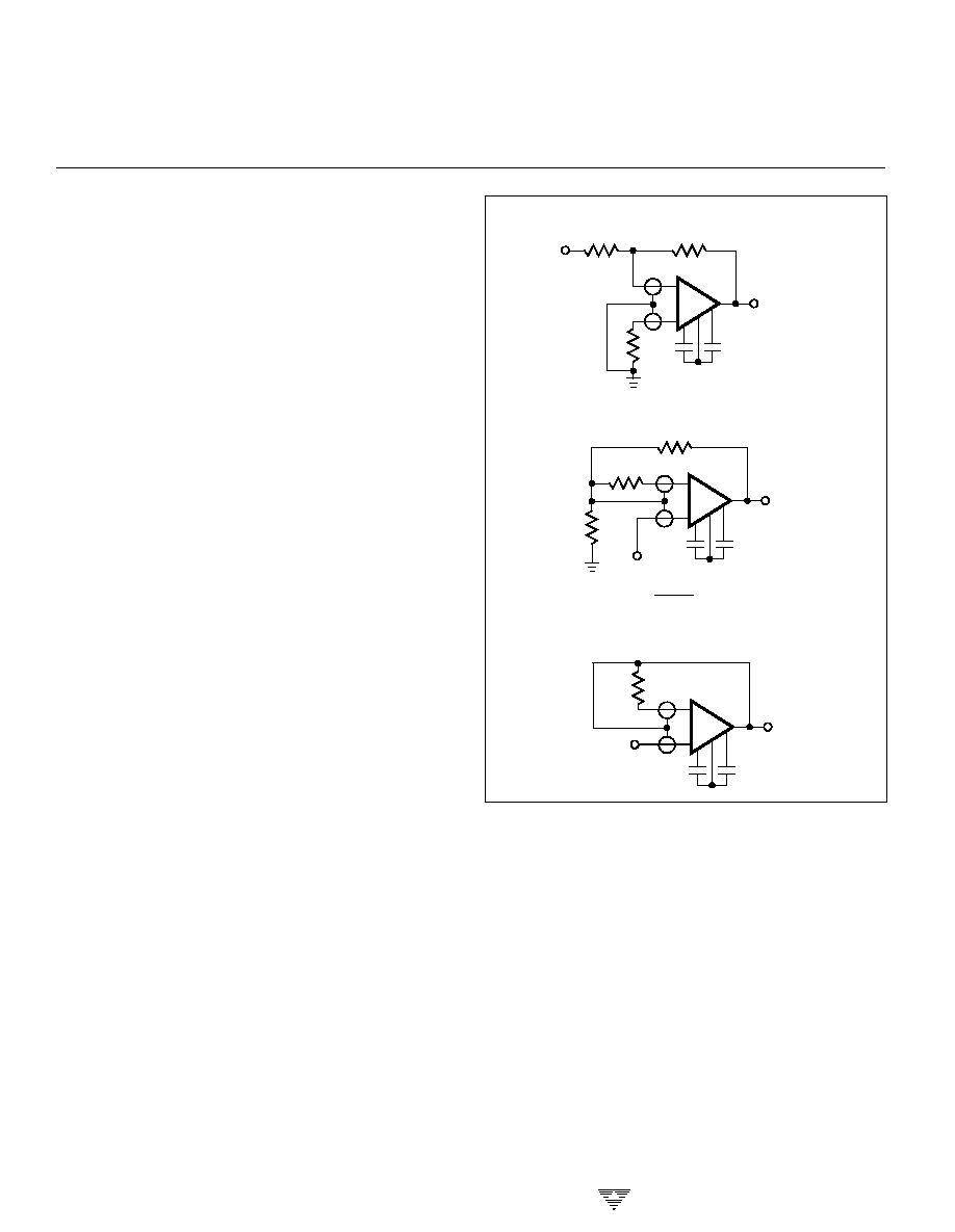
Figure 5. Inverting Amplifier with Optional Clamp
TC7650
CLAMP
+
≠
C
R
C
R1
OUTPUT
0.1 F
µ
0.1 F
µ
INPUT
R2
FOR FULL CLAMP
EFFECT.
( )
R2
R1
100k
*
CONNECT TO V
ON 8-PIN DIP.
*
R
≠
CHOPPER-STABILIZED
OPERATIONAL AMPLIFIER
TC7650
3-278
TELCOM SEMICONDUCTOR, INC.
TC7650
CHOPPER-STABILIZED
OPERATIONAL AMPLIFIER
Figure 6. Input Guard Connection
INPUT
+
≠
OUTPUT
R2
Inverting Amplifier
INPUT
+
≠
OUTPUT
Follower
INPUT
+
≠
OUTPUT
R2
R1
Noninverting Amplifier
R3*
R3*
SHOULD BE LOW
IMPEDANCE FOR
OPTIMUM GUARDING.
NOTE: R =
3
R1 R2
R1 R2
+
R3*
R1
Other operational amplifiers may use this pin as an offset
or compensation point.
The minor modifications needed to retrofit a TC7650
into existing sockets operating at reduced power supply
voltages make prototyping and circuit verification straight-
forward.
Input Guarding
High impedance, low leakage CMOS inputs allow the
TC7650 to make measurements of high-impedance sources.
Stray leakage paths can increase input currents and de-
crease input resistance unless inputs are guarded. A guard
is a conductive PC trace surrounding the input terminals.
The ring connects to a low-impedance point at the same
potential as the inputs. Stray leakages are absorbed by the
low-impedance ring. The equal potential between ring and
inputs prevents input leakage currents. Typical guard con-
nections are shown in Figure 6.
The 14-pin DIP configuration has been specifically
designed to ease input guarding. The pins adjacent to the
inputs are unused.
In applications requiring low leakage currents, boards
should be cleaned thoroughly and blown dry after soldering.
Protective coatings will prevent future board contamination.
Component Selection
The two required capacitors, C
A
and C
B
, have optimum
values, depending on the clock or chopping frequency. For
the preset internal clock, the correct value is 0.1
µ
F. To
maintain the same relationship between the chopping fre-
quency and the nulling time constant, the capacitor values
should be scaled in proportion to the external clock, if used.
High-quality film-type capacitors (such as Mylar) are pre-
ferred; ceramic or other lower-grade capacitors may be
suitable in some applications. For fast settling on initial turn-
on, low dielectric absorption capacitors (such as polypro-
pylene) should be used. With ceramic capacitors, several
seconds may be required to settle to 1
µ
V.
3-279
TELCOM SEMICONDUCTOR, INC.
7
6
5
4
3
1
2
8
CHOPPER-STABILIZED
OPERATIONAL AMPLIFIER
TC7650
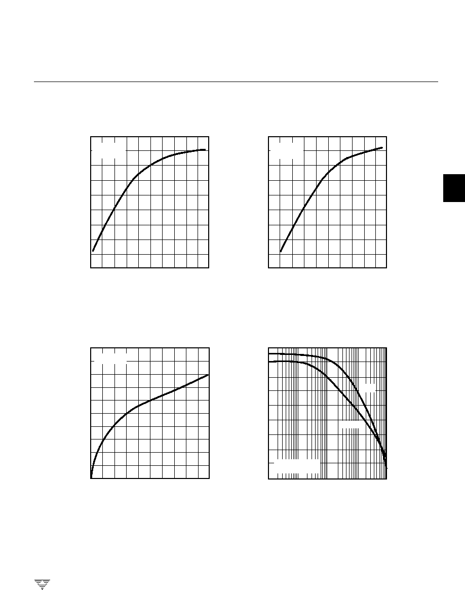
TYPICAL CHARACTERISTICS
4.0 4.1 4.2 4.3 4.4 4.5 4.6 4.7 4.8 4.9 5.0
OUTPUT VOLTAGE (V)
Positive Clamp Current
vs. Output Voltage
CLAMP CURRENT
1 mA
0.1 mA
0.01 mA
1 A
µ
0.1 A
0.01 A
µ
1 nA
1 pA
0.01 nA
0.1 nA
µ
≠4.0 ≠4.1 ≠4.2 ≠4.3 ≠4.4 ≠4.5 ≠4.6 ≠4.7 ≠4.8 ≠4.9 ≠5.0
OUTPUT VOLTAGE (V)
Negative Clamp Current
vs. Output Voltage
CLAMP CURRENT
3.0
2.6
2.2
1.8
1 0
1.4
Supply Current vs.
Supply Voltage
SUPPLY CURRENT (mA)
Gain/Phase vs. Frequency
30
20
10
0
≠10
≠20
≠30
≠40
≠50
≠60
GAIN (dB)
225
180
135
90
45
0
≠45
≠90
≠135
≠180
PHASE (deg)
1 mA
0.1 mA
0.01 mA
1 A
µ
0.1 A
0.01 A
µ
1 nA
1 pA
0.01 nA
0.1 nA
µ
CLOSED-LOOP
GAIN = 20
PHASE
GAIN
T
A
= +25∞C
V
S
= ±5V
T
A
= +25∞C
V
S
= ±5V
T
A
= +25∞C