 | –≠–ª–µ–∫—Ç—Ä–æ–Ω–Ω—ã–π –∫–æ–º–ø–æ–Ω–µ–Ω—Ç: TC7652 | –°–∫–∞—á–∞—Ç—å:  PDF PDF  ZIP ZIP |
Document Outline
- Return to Contents
- List of Figures
- 1. Noninverting Amplifier With Optional Clamp
- 2. Inverting Amplifier With Optional Clamp
- 3. Using 741 to Boost Output Drive Capability
- 4. Low Offset Comparator
- 5. 1437 Offset-Nulled by TC7652
- 6. Splitting +15V With the 7660 at >95% Efficiency
- Features
- Pin Configurations
- Functional Block Diagram
- General Description
- Ordering Information
- Absolute Maximum Ratings
- Electrical Characteristics
- Capacitor Connection
- Output Clamp
- Clock
- Test Circuit
- Application Notes
- Component Selection
- Static Protection
- Latch-Up
- Output Stage/Load Driving
- Thermoelectric Effects
- Guarding
- Pin Compatibility
- Some Applications
- Connection of Input Guards
- Typical Characteristics

3-281
TELCOM SEMICONDUCTOR, INC.
7
6
5
4
3
1
2
8
TC7652
LOW NOISE, CHOPPER-STABILIZED OPERATIONAL AMPLIFIER
FUNCTIONAL BLOCK DIAGRAM
1
2
3
4
8
7
6
5
C
A
OUTPUT
TC7652CPA
≠INPUT
+INPUT
V
SS
V
SS
V
DD
V
DD
C
B
CLAMP
1
2
3
4
5
6
7
14
13
12
11
10
9
8
NC
NC = NO INTERNAL CONNECTION
(MAY BE USED AS INPUT GUARD)
INT/EXT
EXT CLK
IN
INT CLK
OUT
OUTPUT
OUTPUT
CLAMP
RET
C
≠INPUT
+INPUT
NC
TC7652CPD
C
B
C
A
TC7652
NULL
NULL
OUTPUT
B
B
A
C
EXT
C
EXT
C
RET
(NOTE 1)
NULL
AMPLIFIER
MAIN
AMPLIFIER
OUTPUT CLAMP
CIRCUIT
INTERMOD
COMPARATOR
OSCILLATOR
B
A
INT/EXT
EXT CLK IN
CLK OUT
14-PIN DIP ONLY
B
A
INPUTS
OUTPUT CLAMP
(NOT ON "Z" PINOUT)
NOTE: 1. For 8-pin DIP connect to V
SS
, or to C
RET
on "Z" pinout.
V
SS
TC7652-7 9/11/96
FEATURES
s
Low Offset Over Temperature Range ............ 10
µ
V
s
Ultra-Low Long-Term Drift ................. 150nV/Month
s
Low Temperature Drift ............................. 100nV/
∞
C
s
Low DC Input Bias Current ............................. 15pA
s
High Gain, CMRR and PSRR ................. 110dB Min
s
Low Input Noise Voltage ......... 0.2
µ
V
P-P
; DC to 1Hz
s
Internally-Compensated for Unity-Gain Operation
s
Clamp Circuit for Fast Overload Recovery
GENERAL DESCRIPTION
The TC7652 is a lower noise version of the TC7650,
sacrificing some input specifications (bias current and band-
width) to achieve a 10x reduction in noise. All the other
benefits of the chopper technique are present, i.e. freedom
from offset adjust, drift, and reliability problems from exter-
nal trim components. Like the TC7650, the TC7652 re-
quires only two noncritical external caps for storing the
chopped null potentials. There are no significant chopping
spikes, internal effects or overrange lockup problems.
PIN CONFIGURATIONS
ORDERING INFORMATION
Temperature
Part No.
Package Range
TC7652CPA
8-Pin Plastic DIP
0
∞
C to +70
∞
C
TC7652CPD
14-Pin Plastic DIP
0
∞
C to +70
∞
C
3-282
TELCOM SEMICONDUCTOR, INC.
TC7652
LOW NOISE, CHOPPER-STABILIZED
OPERATIONAL AMPLIFIER
ABSOLUTE MAXIMUM RATINGS
*
Total Supply Voltage (V
DD
to V
SS
) ........................... +18V
Input Voltage ........................ (V
DD
+ 0.3V) to (V
SS
≠ 0.3V)
Voltage on Oscillator Control Pins ................... V
DD
to V
SS
Duration of Output Short Circuit ......................... Indefinite
Current Into Any Pin ................................................. 10mA
While Operating (Note 1) ..................................100
µ
A
Package Power Dissipation (T
A
70
∞
C)
8-Pin Plastic DIP ............................................. 730mW
14-Pin Plastic DIP ........................................... 800mW
Storage Temperature Range ................ ≠ 65
∞
C to +150
∞
C
Operating Temperature Range
C Device ................................................ 0
∞
C to +70
∞
C
I Device ............................................. ≠ 25
∞
C to +85
∞
C
Lead Temperature (Soldering, 10 sec) ................. +300
∞
C
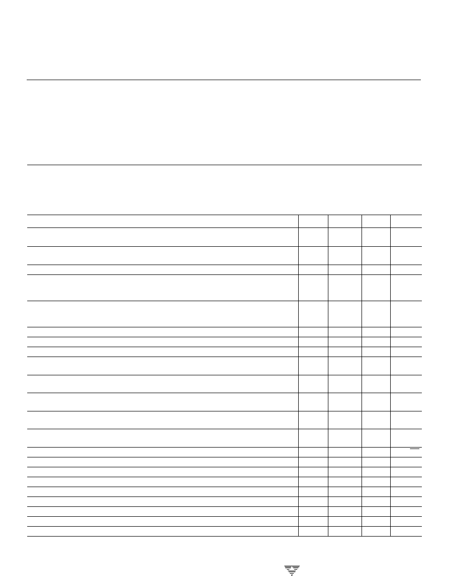
ELECTRICAL CHARACTERISTICS:
V
DD
= +5V, V
SS
= ≠ 5V, T
A
= +25
∞
C, unless otherwise indicated.
Symbol
Parameter
Test Conditions
Min
Typ
Max
Unit
V
OS
Input Offset Voltage
T
A
= +25
∞
C
--
±
2
±
5
µ
V
0
∞
C < T
A
< +70
∞
C
--
±
10
--
TCV
OS
Average Temperature Coefficient of
0
∞
C < T
A
< +70
∞
C
--
0.01
0.05
µ
V/
∞
C
Input Offset Voltage
V
OS
/DT
Offset Voltage vs Time
--
150
--
nV/mo
I
BIAS
Input Bias Current
T
A
= +25
∞
C
--
30
100
pA
(CLK On)
0
∞
C < T
A
< +70
∞
C
--
100
--
≠ 25
∞
C < T
A
< +85
∞
C
--
250
1000
I
BIAS
Input Bias Current
T
A
= +25
∞
C
--
15
30
pA
(CLK Off)
0
∞
C < T
A
< +70
∞
C
--
35
--
≠ 25
∞
C < T
A
< +85
∞
C
--
100
--
I
OS
Input Offset Current
--
25
150
pA
R
IN
Input Resistance
--
10
12
--
W
OL
Large Signal Voltage Gain
R
L
= 10kW, V
OUT
=
±
4V
120
150
--
dB
V
OUT
Output Voltage Swing
R
L
= 10kW
±
4.7
±
4.85
--
V
(Note 2)
R
L
= 100kW
--
±
4.95
--
CMVR
Common-Mode
≠ 4.3
--
+3.5
V
Voltage Range
MRR
Common-Mode
CMVR = ≠ 4.3V to +3.5V
120
140
--
dB
Rejection Ratio
PSRR
Power Supply
±
3V to
±
8V
120
140
--
dB
Rejection Ratio
e
N
Input Noise Voltage
R
S
= 100W, DC to 1Hz
--
0.2
1.5
µ
V
P-P
DC to 10Hz
--
0.7
5
µ
V
P-P
I
N
Input Noise Current
f = 10Hz
--
0.01
--
pA/
Hz
GBW
Unity-Gain Bandwidth
--
0.4
--
MHz
SR
Slew Rate
C
L
= 50 pF, R
L
= 10kW
--
1
--
V/
µ
sec
Overshoot
--
15
--
%
V
DD
, V
SS
Operating Supply Range
5
--
16
V
I
S
Supply Current
No Load
--
1
3
mA
f
CH
Internal Chopping Frequency
Pins 12 ≠ 14 Open (DIP)
100
275
--
Hz
Clamp ON Current (Note 3)
R
L
= 100kW
25
100
--
µ
A
Clamp OFF Current (Note 3)
≠ 4V
V
OUT
< +10V
--
1
--
pA
NOTES: 1. Limiting input current to 100
µ
A is recommended to avoid latch-up problems. Typically, 1mA is safe; however, this is not guaranteed.
2. Output clamp not connected. See typical characteristics curves for output swing versus clamp current characteristics.
*Static-sensitive device. Unused devices must be stored in conductive material. Protect devices from static discharge and static fields. Stresses above
those listed under Absolute Maximum Ratings may cause permanent damage to the device. These are stress ratings only and functional operation of
the device at these or any other conditions above those indicated in the operational sections of the specifications is not implied. Exposure to Absolute
Maximum Rating Conditions for extended periods may affect device reliability.
3-283
TELCOM SEMICONDUCTOR, INC.
7
6
5
4
3
1
2
8
Capacitor Connection
Connect the null-storage capacitors to the C
A
and C
B
pins with a common connection to the C
RET
pin (14-pin
TC7652) or to V
SS
(8-pin TC7652). When connecting to V
SS
,
avoid injecting load current IR drops into the capacitive
circuitry by making this connection directly via a separate
wire or PC trace.
Output Clamp
In chopper-stabilized amplifiers, the output clamp pin
reduces overload recovery time. When a connection is
made to the inverting input pin (summing junction), a current
path is created between that point and the output pin, just
before the device output saturates. This prevents uncon-
trolled differential input voltages and charge buildup on
correction-storage capacitors. Output swing is reduced.
Clock
The TC7652 has a 550Hz internal oscillator, which is
divided by two before clocking the input chopper switches.
The 275Hz chopping frequency is available at INT CLK OUT
(pin 12) on 14-pin devices. In normal operation, INT/EXT
(pin 14), which has an internal pull-up, can be left open.
An external clock can also be used. To disable the
internal clock and use an external one, the INT/EXT pin must
be tied to V
SS
. The external clock signal is then applied to the
EXT CLK IN input (pin 13). An internal divide-by-two pro-
vides a 50% switching duty cycle. The capacitors are only
charged when EXT CLK IN is high, so a 50% to 80% positive
duty cycle is recommended for higher clock frequencies.
The external clock can swing between V
DD
and V
SS
, with the
logic threshold about 2.5V below V
DD
.
The output of the internal oscillator, before the divide-
by-two circuit, is available at EXT CLK IN when INT/EXT is
high or unconnected. This output can serve as the clock
input for a second TC7652 (operating in a master/slave
mode), so that both op amps will clock at the same fre-
quency. This prevents clock intermodulation effects when
two TC7652's are used in a differential amplifier configura-
tion.
If the TC7652's output saturates, error voltages on the
external capacitors will slow overload recovery. This condi-
tion can be avoided if a strobe signal is available. The strobe
signal is applied to EXT CLK IN and the overload signal is
applied to the amplifier while the strobe is LOW. In this case,
neither capacitor will be charged. The low leakage of the
capacitor pins allow long measurements to be made with
negligible errors (typical capacitor drift is 10
µ
V/sec).
APPLICATION NOTES
Component Selection
C
A
and C
B
(external capacitors) should be in the 0.1
µ
F
to 1
µ
F range. For minimum clock ripple noise, use a 1
µ
F
capacitor in broad bandwidth circuits. For limited bandwidth
applications where clock ripple is filtered out, use a 0.1
µ
F
capacitor for slightly lower offset voltage. High-quality film-
type capacitors (polyester or polypropylene) are recom-
mended, although a lower grade (ceramic) may work in
some applications. For quickest settling after initial turn-on,
use low dielectric absorption capacitors (e.g., polypropy-
lene). With ceramic capacitors, settling to 1
µ
V takes
several seconds.
Static Protection
Although input diodes static-protect all device pins,
avoid strong electrostatic fields and discharges that can
cause degraded diode junction characteristics and produce
increased input-leakage currents.
Latch-Up
Junction-isolated CMOS circuits have a 4-layer (p-n-
p-n) structure similar to an SCR. Sometimes this junction
can be triggered into a low-impedance state and produce
excessive supply current. Therefore, avoid applying voltage
greater than 0.3V beyond the supply rails to any pin. Estab-
lish the amplifier supplies at the same time or before any
input signals are applied. If this is not possible, drive circuits
must limit input current flow to under 1mA to avoid latch-up,
even under fault conditions.
Output Stage/Load Driving
The output circuit is high impedance (about 18k
). With
lesser loads, the chopper amplifier behaves somewhat like
a transconductance amplifier with an open-loop gain propor-
tional to load resistance. (For example, the open-loop gain
is 17dB lower with a 1k
load than with a 10k
load.) If the
amp is used only for DC, the DC gain is typically greater than
120dB (even with a 1k
load), and this lower gain is
inconsequential. For wideband, the best frequency response
occurs with a load resistor of at least 10k
. This produces
+
≠
OUTPUT
R2
R1
0.1 µF
0.1 µF
TC7652
C
R
C
1 k
1 M
TEST CIRCUIT
LOW NOISE, CHOPPER-STABILIZED
OPERATIONAL AMPLIFIER
TC7652
3-284
TELCOM SEMICONDUCTOR, INC.
a 6dB/octave response from 0.1Hz to 2MHz, with phase
shifts of less than 2 degrees in the transition region, where
the main amplifier takes over from the null amplifier.
Thermoelectric Effects
The thermoelectric (Seebeck) effects in thermocouple
junctions of dissimilar metals, alloys, silicon, etc. limit ultra-
high-precision DC amplifiers. Unless all junctions are at the
same temperature, thermoelectric voltages around 0.1
µ
V/
∞
C (up to tens of
µ
V/
∞
C for some materials) are generated.
To realize the low offset voltages of the chopper, avoid
temperature gradients. Enclose components to eliminate air
movement, especially from power-dissipating elements in
the system. Where possible, use low thermoelectric-coeffi-
cient connections. Keep power supply voltages and power
dissipation to a minimum. Use high-impedance loads and
seek maximum separation from surrounding heat-dissipat-
ing elements.
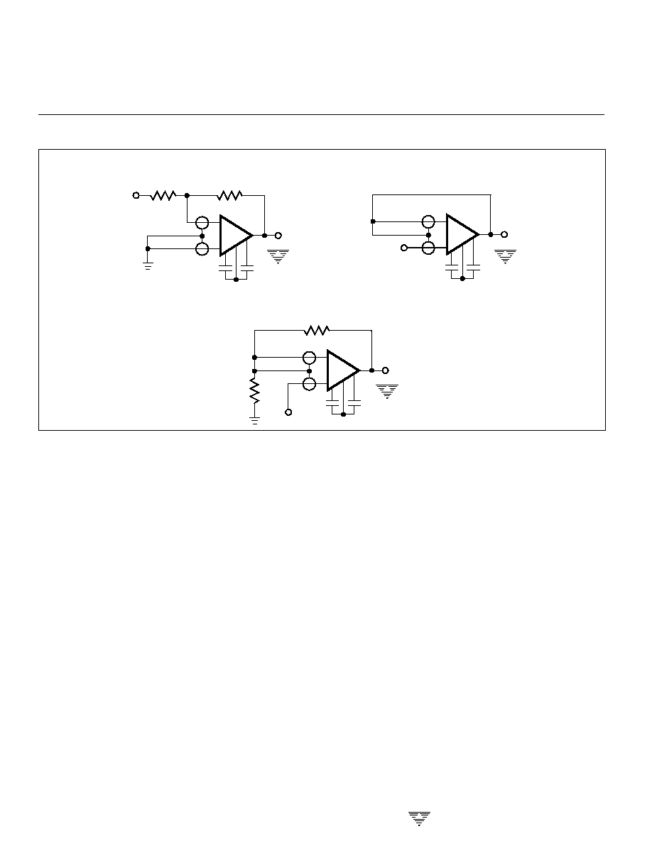
Guarding
To benefit from TC7652 low-input currents, take care
assembling printed circuit boards. Clean boards with alco-
hol or TCE, and blow dry with compressed air. To prevent
contamination, coat boards with epoxy or silicone rubber.
Even if boards are cleaned and coated, leakage cur-
rents may occur because input pins are next to pins at supply
potentials. To reduce this leakage, use guarding to lower the
voltage difference between the inputs and adjacent metal
runs. The guard (a conductive ring surrounding inputs) is
connected to a low-impedance point at about the same
voltage as inputs. The guard absorbs leakage currents from
high-voltage pins.
The 14-pin dual-in-line arrangement simplifies guard-
ing. Like the LM108 pin configuration (but unlike the 101A
and 741), pins next to inputs are not used.
Pin Compatibility
Where possible, the 8-pin device pinout conforms to
such industry standards as the LM101 and LM741. Null-
storing external capacitors connect to pins 1 and 8, which
are usually for offset-null or compensation capacitors. Output
clamp (pin 5) is similarly used. For OP05 and OP07 devices,
replacement of the offset-null potentiometer (connected
between pins 1 and 8 and V
DD
by two capacitors from
those pins to V
SS
) provides compatibility. Replacing the
compensation capacitor between pins 1 and 8 by two
capacitors to V
SS
is required. The same operation (with the
removal of any connection to pin 5) works for LM101,
µ
A748, and similar parts.
Because NC pins provide guarding between input and
other pins, the 14-pin device pinout conforms closely to the
LM108. Because this device does not use any extra pins and
does not provide offset-nulling (but requires a compensation
capacitor), some layout changes are necessary to convert to
the TC7652.
CONNECTION OF INPUT GUARDS
INPUT
+
≠
OUTPUT
R2
R1
Inverting Amplifier
INPUT
+
≠
OUTPUT
Follower
INPUT
+
≠
OUTPUT
R2
R1
Noninverting Amplifier
TC7652
TC7652
TC7652
TC7652
LOW NOISE, CHOPPER-STABILIZED
OPERATIONAL AMPLIFIER

3-285
TELCOM SEMICONDUCTOR, INC.
7
6
5
4
3
1
2
8
Figure 4 shows the clamp circuit of a zero-offset com-
parator. Because the clamp circuit requires the inverting
input to follow the input signal, problems with a chopper-
stabilized op amp are avoided. The threshold input must
tolerate the output clamp current
V
IN
/R without disrupting
other parts of the system.
Figure 5 shows how the TC7652 can offset-null high
slew-rate and wideband amplifiers.
Mixing the TC7652 with circuits operating at
±
15V
requires a lower supply voltage divider with the TC7660
voltage converter circuit operated "backwards." Figure 6
shows an approximate connection.
Figure 6. Splitting +15V With the 7660 at >95% Efficiency
Figure 1. Noninverting Amplifier With Optional Clamp
Figure 2. Inverting Amplifier With Optional Clamp
Figure 5. 1437 Offset-Nulled by TC7652
2
4
5
3
8
TC
7660
6
10 µF
1 M
10 µF
+15V
+7.5V
0V
TC7652
+
≠
OUTPUT
CLAMP
INPUT
0.1 µF
R2
R1
R3
0.1 µF
+
≠
OUTPUT
INPUT
R2
R1
CLAMP
0.1 µF
0.1 µF
TC7652
+
≠
+
≠
+15V
≠15V
≠7.5V
0.1
µF
IN
OUT
≠7.5V
0.1
µF
10 k
TC7652
741
Some Applications
Figures 1 and 2 show basic inverting and noninverting
amplifier circuits using the output clamping circuit to enhance
overload recovery performance. The only limitations on
replacing other op amps with the TC7652 are supply voltage
(
±
8V maximum) and output drive capability (10k
load for
full swing). Overcome these limitations with a booster circuit
(Figure 3) to combine output capabilities of the LM741 (or
other standard device) with input capabilities of the TC7652.
These two form a composite device; therefore, when adding
the feedback network, monitor loop gain stability.
Figure 3. Using 741 to Boost Output Drive Capability
+
≠
TC7652
OUT
IN
+
≠
22 k
22 k
FAST
AMPLIFIER
Figure 4. Low Offset Comparator
TC7652
+
≠
VOUT
CLAMP
VIN
0.1 µF
0.1 µF
200 k
to 2 M
VTH
LOW NOISE, CHOPPER-STABILIZED
OPERATIONAL AMPLIFIER
TC7652

3-286
TELCOM SEMICONDUCTOR, INC.
TYPICAL CHARACTERISTICS
2
3
4
5
6
7
8
±
SUPPLY VOLTAGE (V)
1400
1200
1000
800
600
400
200
0
SUPPLY CURRENT (
µ
A)
Supply Current vs
±
Supply Voltage
1 sec/DIV
2
µ
V/DIV
Noise at 0.1 Hz to 10 Hz
OUTPUT VOLTAGE (V)
4.0 4.1 4.2 4.3 4.4 4.5 4.6 4.7 4.8 4.9 5.0
1 mA
0.1 mA
0.01 mA
1
µ
A
0.1
µ
A
0.01
µ
A
1 nA
0.1 nA
0.01 nA
1 pA
CLAMP CURRENT
Positive Clamp Current
1 sec/DIV
1
µ
V/DIV
Noise at 0.1 Hz to 1 Hz
OUTPUT VOLTAGE (V)
4.0 4.1 4.2 4.3 4.4 4.5 4.6 4.7 4.8 4.9 5.0
1 mA
0.1 mA
0.01 mA
1
µ
A
0.1
µ
A
0.01
µ
A
1 nA
0.1 nA
0.01 nA
1 pA
CLAMP CURRENT
Negative Clamp Current
1
10
100
1k
10k
100k
1M
FREQUENCY (Hz)
GAIN
≠20
≠10
0
10
20
30
40
60
GAIN (dB)
Phase-Gain (Bode Plot)*
*NOTE:
±
5V,
±
2.5V supplies; no load to 10k load.
≠180
≠120
≠60
+60
+120
+180
+240
50
PHASE (deg)
0
1 sec/DIV
1
µ
V/DIV
Noise at 0.1 Hz to 100 Hz
5
µ
sec/DIV
0.5V/DIV
Slew Rate
SOURCE
SINK
Output Resistance
vs Output Voltage
100
OUTPUT RESISTANCE (
)
≠3.0
OUTPUT VOLTAGE (V)
1k
10k
100k
1M
≠5.0
≠4.0
≠6
≠4
≠2
0
2
4
COMMON-MODE VOLTAGE (V)
Input Offset Voltage vs Common-Mode Voltage
4.0
3.5
3.0
2.5
2.0
1.5
1.0
0.5
INPUT OFFSET
VOLTAGE (
µ
V)
PHASE
TC7652
LOW NOISE, CHOPPER-STABILIZED
OPERATIONAL AMPLIFIER