 | –≠–ª–µ–∫—Ç—Ä–æ–Ω–Ω—ã–π –∫–æ–º–ø–æ–Ω–µ–Ω—Ç: TC911A | –°–∫–∞—á–∞—Ç—å:  PDF PDF  ZIP ZIP |
Document Outline
- Return to Contents
- List of Figures
- 1. Unwanted Thermocouple Errors Eliminated by Reducing Thermal Gradients and Balancing Junctions
- Features
- Ordering Information
- Functional Block Diagram
- General Description
- Pin Configuration
- Absolute Maximum Ratings
- Electrical Characteristics
- Typical Characteristics
- Pin Compatibility
- Thermocouple Errors
- Avoiding Latch-Up
- Overload Recovery
- Typical Applications
3-263
TELCOM SEMICONDUCTOR, INC.
7
6
5
4
3
1
2
8
AUTO-ZEROED OPERATIONAL AMPLIFIERS
FEATURES
s
First Monolithic Chopper-Stabilized Amplifier
With On-Chip Nulling Capacitors
s
Offset Voltage .................................................... 5
µ
V
s
Offset Voltage Drift .................................. 0.05
µ
V/
∞
C
s
Low Supply Current ...................................... 350
µ
A
s
High Common-Mode Rejection .................... 116dB
s
Single Supply Operation ....................... 4.5V to 16V
s
High Slew Rate ............................................. 2.5V/
µ
s
s
Wide Bandwidth ............................................ 1.5MHz
s
High Open-Loop Voltage Gain
(R
L
= 10 k
) .................................................... 120dB
s
Low Input Voltage Noise
(0.1 Hz to 1 Hz) .......................................... 0.65
µ
V
P-P
s
Pin Compatible With ICL7650
s
Lower System Parts Count
GENERAL DESCRIPTION
The TC911 CMOS auto-zeroed operational amplifier is
the first complete monolithic chopper-stabilized amplifier.
Chopper operational amplifiers like the ICL7650/7652 and
LTC1052 require user-supplied, external offset compensa-
tion storage capacitors. External capacitors are not re-
quired with the TC911. Just as easy to use as the conven-
tional OP07 type amplifier, the TC911 significantly reduces
offset voltage errors. Pinout matches the OP07/741/7650
8-pin mini-DIP configuration.
Several system benefits arise by eliminating the exter-
nal chopper capacitors: lower system parts count, reduced
assembly time and cost, greater system reliability, reduced
PC board layout effort and greater board area utilization.
Space savings can be significant in multiple-amplifier de-
signs.
Electrical specifications include 15
µ
V maximum offset
voltage, 0.15
µ
V/
∞
C maximum offset voltage temperature
coefficient. Offset voltage error is five times lower than the
premium OP07E bipolar device. The TC911 improves off-
set drift performance by eight times.
The TC911 operates from dual or single power sup-
plies. Supply current is typically 350
µ
A. Single 4.5V to 16V
supply operation is possible, making single 9V battery
operation possible. The TC911 is available in 2 package
types: 8-pin plastic DIP and SOIC.
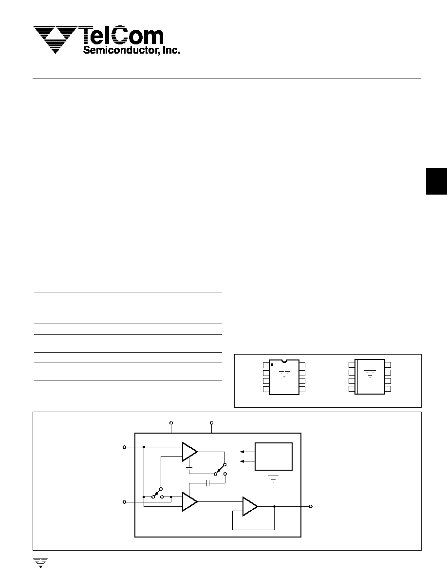
PIN CONFIGURATION (SOIC and DIP)
+
≠
+
≠
VDD
VSS
TC911
≠INPUT
+INPUT
A
2
3
4
7
B
*
*
A
B
6
*
NOTE: Internal capacitors. No external capacitors required.
MAIN
AMPLIFIER
LOW IMPEDANCE
OUTPUT BUFFER
INTERNAL
OSCILLATOR
(f 200 Hz)
OSC
V CORRECTION AMPLIFIER
OS
+
≠
OUTPUT
1
2
3
4
8
7
6
5
OUTPUT
NC
+ INPUT
TC911ACPA
TC911BCPA
≠ INPUT
NC
NC
V
SS
V
SS
V
DD
V
DD
NC = NO INTERNAL CONNECTION
1
2
3
4
8
7
6
5
OUTPUT
NC
+ INPUT
TC911ACOA
TC911BCOA
≠ INPUT
NC
NC
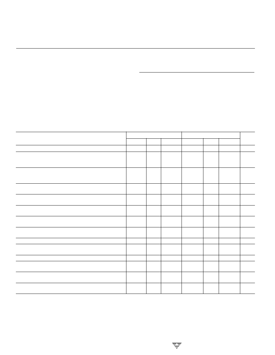
ORDERING INFORMATION
Maximum
Temperature
Offset
Part No.
Package
Range
Voltage
TC911ACOA
8-Pin SOIC
0
∞
C to +70
∞
C
15
µ
V
TC911ACPA
8-Pin
0
∞
C to +70
∞
C
15
µ
V
Plastic DIP
TC911BCOA
8-Pin SOIC
0
∞
C to +70
∞
C
30
µ
V
TC911BCPA
8-Pin
0
∞
C to +70
∞
C
30
µ
V
Plastic DIP
FUNCTIONAL BLOCK DIAGRAM
TC911/A/B-7 9/11/96
TC911A
TC911B
3-264
TELCOM SEMICONDUCTOR, INC.
AUTO-ZEROED MONOLITHIC
OPERATIONAL AMPLIFIERS
TC911A
TC911B
ABSOLUTE MAXIMUM RATINGS*
Total Supply Voltage (V
DD
to V
SS
) ........................... +18V
Input Voltage ........................ (V
DD
+ 0.3V) to (V
SS
≠ 0.3V)
Current into Any Pin ................................................. 10mA
While Operating ................................................ 100
µ
A
Storage Temperature Range ................ ≠ 65
∞
C to +150
∞
C
Lead Temperature (Soldering, 10 sec) ................. +300
∞
C
Operating Temperature Range
C Device ................................................ 0
∞
C to +70
∞
C
Package Power Dissipation (T
A
=
70
∞
C)
Plastic DIP ...................................................... 730mW
Plastic SOIC ................................................... 470mW
*Static-sensitive device. Unused devices should be stored in conductive
material. Stresses above those listed under "Absolute Maximum Ratings"
may cause permanent damage to the device. These are stress ratings only
and functional operation of the device at these or any other conditions
above those indicated in the operational sections of the specifications is not
implied.
ELECTRICAL CHARACTERISTICS:
V
S
=
±
5V, T
A
= +25
∞
C, unless otherwise indicated.
TC911A
TC911B
Symbol Parameter
Test Conditions
Min
Typ
Max
Min
Typ
Max
Unit
V
OS
Input Offset Voltage
T
A
= +25
∞
C
--
5
15
--
15
30
µ
V
TCV
OS
Average Temperature
0
∞
C
T
A
+70
∞
C
--
0.05
0.15
--
0.1
0.25
µ
V/
∞
C
Coefficient of Input
≠25
∞
C
T
A
+85
∞
C
--
0.05
0.15
--
0.1
0.25
µ
V/
∞
C
Offset Voltage
(Note 1)
I
B
Average Input Bias
T
A
= +25
∞
C
--
--
70
--
--
120
pA
Current
0
∞
C
T
A
+70
∞
C
--
--
3
--
--
4
nA
≠25
∞
C
T
A
+85
∞
C
--
--
4
--
--
6
nA
I
OS
Average Input
T
A
= +25
∞
C
--
5
20
--
10
40
pA
Offset Current
T
A
= +85
∞
C
--
--
1
--
--
1
nA
e
N
Input Voltage Noise
0.1 to 1 Hz, R
S
100
--
0.65
--
--
0.65
--
µ
V
P-P
0.1 to 10 Hz, R
S
100
--
11
--
--
11
--
µ
V
P-P
CMRR
Common-Mode
V
SS
V
CM
V
DD
≠ 2.2
110
116
--
105
110
--
dB
Rejection Ratio
CMVR
Common-Mode
V
SS
--
V
DD
≠ 2
V
SS
--
V
DD
≠ 2
V
Voltage Range
A
OL
Open-Loop Voltage
R
L
= 10 k
, V
OUT
=
±
4V
115
120
--
110
120
--
dB
Gain
V
OUT
Output Voltage Swing
R
L
= 10 k
V
SS
+ 0.3
--
V
DD
≠ 0.9
V
SS
+ 0.3
--
V
DD
≠ 0.9
V
BW
Closed Loop
Closed Loop Gain = +1
--
1.5
--
--
1.5
--
MHz
Bandwidth
SR
Slew Rate
R
L
= 10 k
, C
L
= 50 pF
--
2.5
--
--
2.5
--
V/
µ
s
PSRR
Power Supply
±
3.3V to
±
5.5V
112
--
--
105
--
--
dB
Rejection Ratio
V
S
Operating Supply
Split Supply
±
3.3
--
±
8
±
3.3
--
±
8
V
Voltage Range
Single Supply
6.5
--
16
6.5
--
16
V
I
S
Quiescent Supply
V
S
=
±
5V
--
350
600
--
--
800
µ
A
Current
NOTES: 1. Characterized; not 100% tested.
3-265
TELCOM SEMICONDUCTOR, INC.
7
6
5
4
3
1
2
8
AUTO-ZEROED MONOLITHIC
OPERATIONAL AMPLIFIERS
TC911A
TC911B
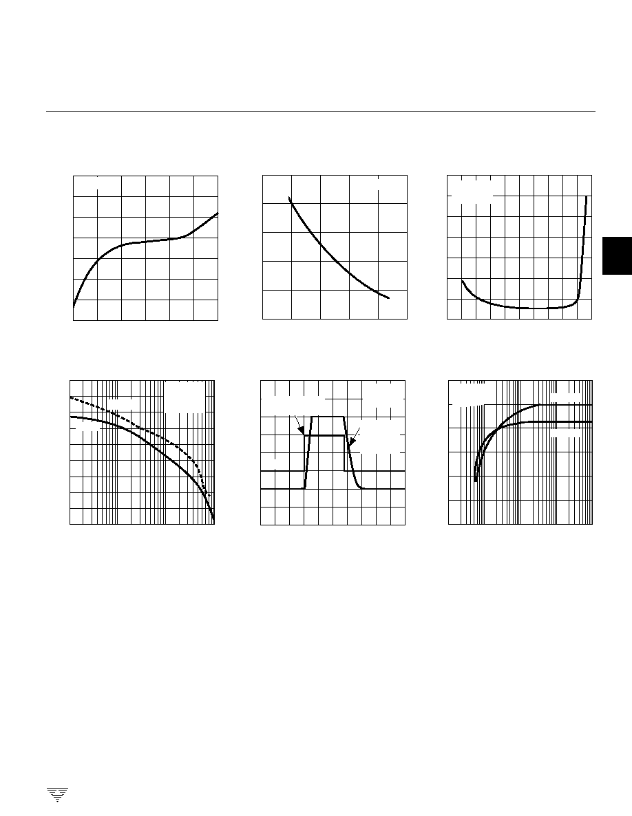
TYPICAL CHARACTERISTICS
450
SUPPLY CURRENT (
µ
A)
≠100
AMBIENT TEMPERATURE (
∞
C)
400
350
300
250
200
≠50
0
50
100
150
Supply Current vs. Temperature
V
S
=
±
5V
HORIZONTAL SCALE = 2
µ
s/DIV
Large Signal Output
Switching Waveform
R
L
= 10 k
T
A
= +25
∞
C
0V
INPUT VERTICAL
SCALE = 2 V/DIV
OUTPUT
VERTICAL
SCALE
= 1 V/DIV
35
INPUT OFFSET VOLTAGE (
µ
V)
≠6
INPUT COMMON-MODE VOLTAGE (V)
Input Offset Voltage vs.
Common-Mode Voltage
30
25
20
15
10
5
0
≠5 ≠4 ≠3 ≠2 ≠1
0
1
2
3
4
V
S
=
±
5V
T
A
= +25
∞
C
700
600
500
400
300
200
100
0
SUPPLY CURRENT (
µ
A)
2
3
4
5
6
7
8
±
SUPPLY VOLTAGE (V)
T
A
= +25
∞
C
Supply Current vs.
±
Supply Voltage
50
CLOSED-LOOP GAIN (dB)
10k
FREQUENCY (Hz)
Gain and Phase vs. Frequency
40
30
20
10
0
≠10
≠20
≠30
≠40
100k
1M
10M
PHASE
GAIN
V
S
=
±
5V
T
A
= +25
∞
C
R
L
= 10 k
225
PHASE (deg)
180
135
90
45
0
≠45
≠90
≠135
≠180
±
OUTPUT VOLTAGE (V)
100
LOAD RESISTANCE (
)
Output Voltage Swing vs.
Load Resistance
5.0
V
S
=
±
5V
T
A
= +25
∞
C
≠SWING
+SWING
4.2
3.4
2.6
1.8
1.0
1k
10k
100k
1M
5.8

3-266
TELCOM SEMICONDUCTOR, INC.
AUTO-ZEROED MONOLITHIC
OPERATIONAL AMPLIFIERS
TC911A
TC911B
Pin Compatibility
The CMOS TC911 is pin compatible with the industry
standard ICL7650 chopper-stabilized amplifier. The ICL7650
must use external 0.1
µ
F capacitors connected at pins 1 and
8. With the TC911, external offset voltage error cancel-
ing capacitors are not required. On the TC911 pins 1, 8
and 5 are not connected internally. The ICL7650 uses pin 5
as an optional output clamp connection. External chopper
capacitors and clamp connections are not necessary with
the TC911. External circuits connected to pins 1, 8 and 5 will
have no effect. The TC911 can be quickly evaluated in
existing ICL7650 designs. Since external capacitors are not
required, system part count, assembly time, and total sys-
tem cost are reduced. Reliability is increased and PC board
layout eased by having the error storage capacitors inte-
grated on the TC911 chip.
The TC911 pinout matches many existing op amps:
741, LM101, LM108, OP05≠OP08, OP-20, OP-21, ICL7650
and ICL7652. In many applications operating from +5V
supplies the TC911 offers superior electrical performance
and can be a functional pin-compatible replacement. Offset
voltage correction potentiometers, compensation capaci-
tors, and chopper-stabilization capacitors can be removed
when retrofitting existing equipment designs.
Thermocouple Errors
Heating one joint of a loop made from two different
metallic wires causes current flow. This is known as the
Seebeck effect. By breaking the loop, an open circuit voltage
(Seebeck voltage) can be measured. Junction temperature
and metal type determine the magnitude. Typical values are
0.1
µ
V/
∞
C to 10
µ
V/
∞
C. Thermal-induced voltages can be
many times larger than the TC911 offset voltage drift. Unless
unwanted thermocouple potentials can be controlled, sys-
tem performance will be less than optimum.
Unwanted thermocouple junctions are created when
leads are soldered or sockets/connectors are used. Low
thermo-electric coefficient solder can reduce errors. A 60%
Sn/36% Pb solder has 1/10 the thermal voltage of common
64% Sn/36% Pb solder at a copper junction.
The number and type of dissimilar metallic junctions in
the input circuit loop should be balanced. If the junctions are
kept at the same temperature, their summation will add to
zero-canceling errors (Figure 1).
Shielding precision analog circuits from air currents --
especially those caused by power dissipating components
and fans -- will minimize temperature gradients and ther-
mocouple-induced errors.
Avoiding Latch-Up
Junction-isolated CMOS circuits inherently contain a
parasitic p-n-p-n transistor circuit. Voltages exceeding the
supplies by 0.3V should not be applied to the device pins.
Larger voltages can turn the p-n-p-n device on, causing
excessive device power supply current and excessive power
dissipation. TC911 power supplies should be established at
the same time or before input signals are applied. If this is not
possible input current should be limited to 0.1mA to avoid
triggering the p-n-p-n structure.
Overload Recovery
The TC911 recovers quickly from the output saturation.
Typical recovery time from positive output saturation is
20msec. Negative output saturation recovery time is typi-
cally 5msec.
Figure 1. Unwanted Thermocouple Errors Eliminated by
Reducing Thermal Gradients and Balancing Junctions
J3
J4
J5
J2
J1
J6
PACKAGE
PIN
J = J
J = J
J = J
3
2
1
4
5
6
NO TEMPERATURE DIFFERENTIAL
AND SAME METALLIC CONNECTION
+
≠
≠
+
+
≠
+
≠
+
≠
+
≠
V2
V1
V5
V6
V4
V3
J4
J3
J2
J1
J5
J6
V = 0
T
V = V + V + V ≠ V ≠ V ≠ V = 0
T
1
2
3
4
5
6

3-267
TELCOM SEMICONDUCTOR, INC.
7
6
5
4
3
1
2
8
AUTO-ZEROED MONOLITHIC
OPERATIONAL AMPLIFIERS
TC911A
TC911B
TYPICAL APPLICATIONS
Thermometer Circuit
10-Volt Precision Reference
+
≠
TC911
18 k
6.4 k
3.6 k
6.4V
4
6
7
3
2
0.1 µF
+15V
V = 10V
OUT
+9V
TC911
REF02
≠
+
VOUT
R
2
R
3
R
1
ADJ
TEMP
OUT
V
REF
V = V
OUT
1 + R
2
[
(
)
V
REF
≠
] [
R
2
]
1 + R
2
[
R + R
1
1
(
)]
d (V )
d V
OUT
=
K (2.1 mV/
∞
C)
K = 1 +
R
2
dT
R X R
TEMP
TEMP
3
3
dT
R + R
1
3
R
1
1
R X R
3
1
R X R
3
Programmable Gain Amplifier With Input Multiplexer
+
≠
IN1
TC911
IN2
IN3
A1 A2 A3 A4WR
+5V
≠5V
GND
+5V ≠5V
+5V
≠5V
1
VOUT
2 k
18 k
INPUT
CHANNEL
SELECT
68HC11
GAIN
SELECT
A1 A2 A3 A4
WR
LATCH
GND
10
X
100
1000
X
X
X
99 k
999 k
1 k
1 k
IN4
IC1b
IC1b
IC1a, b, = Quad Analog Switch