 | –≠–ª–µ–∫—Ç—Ä–æ–Ω–Ω—ã–π –∫–æ–º–ø–æ–Ω–µ–Ω—Ç: TC913ACPA | –°–∫–∞—á–∞—Ç—å:  PDF PDF  ZIP ZIP |
Document Outline
- Return to Contents
- Features
- Ordering Information
- Pin Configuration
- General Description
- Functional Block Diagram
- Absolute Maximum Ratings
- Electrical Characteristics
- Theory of Operation
- Pin Compatibility
- Overload Recovery
- Avoiding Latch-Up
- Typical Characteristics

3-269
TELCOM SEMICONDUCTOR, INC.
7
6
5
4
3
1
2
8
DUAL AUTO-ZEROED OPERATIONAL AMPLIFIERS
FEATURES
s
First Monolithic Dual Auto-Zeroed Operational
Amplifier
s
Chopper Amplifier Performance Without External
Capacitors
-- V
OS
........................................................ 15
µ
V Max
-- V
OS
Drift ....................................... 0.15
µ
V/
∞
C Max
-- Saves Cost/Assembly of Four "Chopper"
Capacitors
s
SOIC Packages Available
s
High DC Gain ................................................. 120dB
s
Low Supply Current ...................................... 650
µ
A
s
Low Input Voltage Noise
(0.1 Hz to 10 Hz) ........................................ 0.65
µ
V
P-P
s
Wide Common-Mode
Voltage Range ................................. V
SS
to V
DD
≠ 2V
s
High Common-Mode Rejection .................... 116dB
s
Dual or Single Supply Operation ....
±
3.3V to
±
8.3V
+6.5V to +16V
s
Excellent AC Operating Characteristics
-- Slew Rate ............................................. 2.5V/
µ
sec
-- Unity-Gain Bandwidth ............................. 1.5MHz
s
Pin Compatible With LM358, OP-14, MC1458,
ICL7621, TL082, TLC322
GENERAL DESCRIPTION
The TC913 is the world's first complete monolithic,
dual auto-zeroed operational amplifier. The TC913 sets a
new standard for low-power, precision dual-operational
amplifiers. Chopper-stabilized or auto-zeroed amplifiers
offer low offset voltage errors by periodically sampling
offset error, and storing correction voltages on capacitors.
Previous single amplifier designs required two user-sup-
plied, external 0.1
µ
F error storage correction capacitors --
much too large for on-chip integration. The unique TC913
architecture requires smaller capacitors, making on-chip
integration possible. Microvolt offset levels are achieved
and external capacitors are not required.
The TC913 system benefits are apparent when con-
trasted with a TC7650 chopper amplifier circuit implemen-
tation. A single TC913 replaces two TC7650's and four
capacitors. Five components and assembly steps are elimi-
nated.
The TC913 pinout matches many popular dual-
operational amplifiers: OP-04, TLC322, LM358, and
ICL7621 are typical examples. In many applications,
operating from dual 5V power supplies or single supplies,
the TC913 offers superior electrical performance, and can
be a functional drop-in replacement; printed circuit board
rework is not necessary. The TC913's low offset voltage
error eliminates offset voltage trim potentiometers often
needed with bipolar and low-accuracy CMOS operational
amplifiers.
The TC913 takes full advantage of TelCom's propri-
etary CMOS technology. Unity gain bandwidth is 1.5 MHz
and slew rate is 2.5 V/
µ
sec.
≠
+
+
≠
VDD
VSS
TC913
A
4
8
B
*
A
B
*NOTE: Internal capacitors. No external capacitors required.
MAIN
AMPLIFIER
LOW IMPEDANCE
OUTPUT BUFFER
INTERNAL
OSCILLATOR
(f 200 Hz)
OSC
V CORRECTION AMPLIFIER
OS
+
≠
≠INPUT A
≠INPUT B
1 OF 2 AMPLIFIERS SHOWN
OUTPUT A
2
6
≠INPUT A
≠INPUT B
3
5
OUTPUT B
7
1
*
FUNCTIONAL BLOCK DIAGRAM
ORDERING INFORMATION
Maximum
Temp.
Offset
Part No.
Package
Range
Voltage
TC913ACOA
8-Pin SOIC
0
∞
C to +70
∞
C
15
µ
V
TC913ACPA
8-Pin Plastic DIP
0
∞
C to +70
∞
C
15
µ
V
TC913BCOA
8-Pin SOIC
0
∞
C to +70
∞
C
30
µ
V
TC913BCPA
8-Pin Plastic DIP
0
∞
C to +70
∞
C
30
µ
V
PIN CONFIGURATION (SOIC and DIP)
1
2
3
4
6
5
≠IN B
7
8
OUT A
≠IN A
+IN A
V
SS
V
SS
VDD
VDD
+IN B
TC913ACPA
TC913BCPA
TC913ACOA
TC913BCOA
OUT B
+
≠
≠
+
A
B
1
2
3
4
6
5
≠IN B
7
8
OUT A
≠IN A
+IN A
+IN B
OUT B
+
≠
≠
+
A
B
TC913A/B-8 9/3/96
TC913A
TC913B

3-270
TELCOM SEMICONDUCTOR, INC.
DUAL AUTO-ZEROED
OPERATIONAL AMPLIFIERS
TC913A
TC913B
ABSOLUTE MAXIMUM RATINGS*
Total Supply Voltage (V
DD
to V
SS
) .......................... +18V
Input Voltage ........................ (V
DD
+ 0.3V) to (V
SS
≠ 0.3V)
Current into Any Pin ................................................. 10mA
While Operating ................................................ 100
µ
A
Storage Temperature Range ................ ≠ 65
∞
C to +150
∞
C
Lead Temperature (Soldering, 10 sec) ................. +300
∞
C
Operating Temperature Range
C Device ................................................ 0
∞
C to +70
∞
C
Package Power Dissipation (T
A
=
70
∞
C)
Plastic SOIC ................................................... 470mW
Plastic DIP ...................................................... 730mW
*Static-sensitive device. Unused devices should be stored in conductive
material. Stresses above those listed under "Absolute Maximum Ratings"
may cause permanent damage to the device. These are stress ratings only
and functional operation of the device at these or any other conditions
above those indicated in the operational sections of the specifications is not
implied.
ELECTRICAL CHARACTERISTICS:
V
S
=
±
5V, T
A
= +25
∞
C, unless otherwise indicated.
TC913A
TC913B
Symbol Parameter
Test Conditions
Min
Typ
Max
Min
Typ
Max
Unit
V
OS
Input Offset Voltage
T
A
= +25
∞
C
--
5
15
--
15
30
µ
V
TCV
OS
Average Temperature 0
∞
C
T
A
+70
∞
C
--
0.05
0.15
--
0.1
0.25
µ
V/
∞
C
Coefficient of Input
≠25
∞
C
T
A
+85
∞
C
--
0.05
0.15
--
0.1
0.25
µ
V/
∞
C
Offset Voltage
(Note 1)
I
B
Average Input Bias
T
A
= +25
∞
C
--
--
90
--
--
120
pA
Current
0
∞
C
T
A
+70
∞
C
--
--
3
--
--
4
nA
≠25
∞
C
T
A
+85
∞
C
--
--
4
--
--
6
nA
I
OS
Average Input
T
A
= +25
∞
C
--
5
20
--
10
40
pA
Offset Current
T
A
= +85
∞
C
--
--
1
--
--
1
nA
e
N
Input Voltage Noise
0.1 to 1 Hz, R
S
100
--
0.6
--
--
0.6
--
µ
V
P-P
0.1 to 10 Hz, R
S
100
--
11
--
--
11
--
µ
V
P-P
CMRR
Common-Mode
V
SS
V
CM
V
DD
≠ 2.2V
110
116
--
100
110
--
dB
Rejection Ratio
CMVR
Common-Mode
V
SS
--
V
DD
≠ 2
V
SS
--
V
DD
≠ 2
V
Voltage Range
A
OL
Open-Loop Voltage
R
L
= 10 k
, V
O
=
±
4V
115
120
--
110
120
--
dB
Gain
V
OUT
Output Voltage Swing R
L
= 10 k
V
SS
+ 0.3
--
V
DD
≠ 0.9
V
SS
+ 0.3
--
V
DD
≠ 0.9
V
BW
Closed-Loop
Closed Loop Gain = +1
--
1.5
--
--
1.5
--
MHz
Bandwidth
SR
Slew Rate
R
L
= 10 k
, C
L
= 50 pF
--
2.5
--
--
2.5
--
V/
µ
s
PSRR
Power Supply
±
3.3V
V
S
±
5.5V
110
--
--
100
--
--
dB
Rejection Ratio
V
S
Operating Supply
Split Supply
±
3.3
--
±
8.3
±
3.3
--
±
8.3
V
Voltage Range
Single Supply
6.5
--
16
6.5
--
16
V
I
S
Quiescent Supply
V
S
=
±
5V
--
0.65
0.85
--
--
1.1
mA
Current
NOTE:
1. Characterized; not 100% tested.

3-271
TELCOM SEMICONDUCTOR, INC.
7
6
5
4
3
1
2
8
DUAL AUTO-ZEROED
OPERATIONAL AMPLIFIERS
TC913A
TC913B
Theory of Operation
Each of the TC913's two op-amps actually consists of
two amplifiers. A main amplifier is always connected from
the input to the output. A separate nulling amplifier alter-
nately nulls its own offset and then the offset of the amplifier.
Since each amplifier is continuously being nulled, offset
voltage drift with time, temperature, and power supply
variations is greatly reduced.
All nulling circuitry is internal and the nulling operation is
transparent to the user. Offset nulling voltages are stored on
two internal capacitors. An internal oscillator and control
logic, shared by the TC913's two amplifiers, control the
nulling process.
Pin Compatibility
The TC913 pinout is compatible with OP-14, LM358,
MC1458, LT1013, TLC322, and similar dual op amps. In
many circuits operating from single or
±
5V supplies, the
TC913 is a drop-in replacement offering DC performance
rivaling that of the best single op amps.
The TC913's amplifiers include a low-impedance class
AB output buffer. Some previous CMOS chopper amplifiers
used a high-impedance output stage which made open-loop
gain dependent on load resistance. The TC913's open-loop
gain is not dependent on load resistance.
Overload Recovery
The TC913 recovers quickly from output saturation.
Typical recovery time from positive output saturation is
20msec. Negative output saturation recovery time is typi-
cally 5msec.
Avoiding Latch-Up
Junction-isolated CMOS circuits inherently contain a
parasitic p-n-p-n transistor circuit. Voltages exceeding the
supplies by 0.3V should not be applied to the device pins.
Larger voltages can turn the p-n-p-n device on, causing
excessive device power supply current and power dissipa-
tion. The TC913's power supplies should be established at
the same time or before input signals are applied. If this is
not possible, input current should be limited to 0.1mA to
avoid triggering the p-n-p-n structure.
3-272
TELCOM SEMICONDUCTOR, INC.
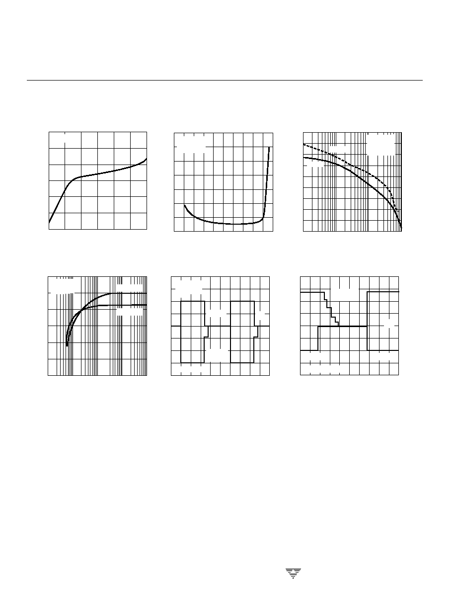
HORIZONTAL SCALE = 20 msec/DIV
Positive Overload Recovery Time
0V
OUTPUT =
2 V/DIV
INPUT
INPUT
GAIN = ≠20
35
INPUT OFFSET VOLTAGE (
µ
V)
≠6
INPUT COMMON-MODE VOLTAGE (V)
Input Offset Voltage vs.
Common-Mode Voltage
30
25
20
15
10
5
0
≠5 ≠4 ≠3 ≠2 ≠1
0
1
2
3
4
V =
±
5V
T = +25
∞
C
S
A
SUPPLY CURRENT (
µ
A)
±
SUPPLY VOLTAGE (V)
Supply Current vs.
±
Supply Voltage
HORIZONTAL SCALE = 20 msec/DIV
Negative Overload Recovery Time
R = 10 k
T = +25
∞
C
INPUT
0V
L
A
OUTPUT
= 2 V/DIV
50
CLOSED-LOOP GAIN (dB)
10k
FREQUENCY (Hz)
Gain and Phase vs. Frequency
40
30
20
10
0
≠10
≠20
≠30
≠40
100k
1M
10M
PHASE
GAIN
V =
±
5V
T = +25
∞
C
R = 10 k
225
PHASE (deg)
180
135
90
45
0
≠45
≠90
≠135
≠180
±
OUTPUT VOLTAGE (V)
100
LOAD RESISTANCE (
)
Output Voltage Swing vs.
Load Resistance
5.0
V =
±
5V
T = +25
∞
C
≠SWING
+SWING
4.2
3.4
2.6
1.8
1.0
1k
10k
100k
1M
A
S
S
A
L
1200
1000
800
600
400
200
0
2
3
5
4
6
7
8
T = +25
∞
C
A
GAIN = ≠20
TYPICAL CHARACTERISTICS
TC913A
TC913B
DUAL AUTO-ZEROED
OPERATIONAL AMPLIFIERS