 | –≠–ª–µ–∫—Ç—Ä–æ–Ω–Ω—ã–π –∫–æ–º–ø–æ–Ω–µ–Ω—Ç: TC9401CPD | –°–∫–∞—á–∞—Ç—å:  PDF PDF  ZIP ZIP |
Document Outline
- Return to Contents
- List of Figures
- 1. 10 Hz to 10 kHz V/F Converter
- 2 . Output Waveforms
- 3. Recommended CREF vs VREF
- 4 . Fixed Voltage Ñ Single Supply Operation
- 5. Voltage to Frequency
- 6. Frequency Input Level Shifter
- 7. DC Ñ 10 kHz F/V Converter
- 8 . F/V Digital Outputs
- 9. F/V Single Supply F/V Converter
- 10. Ripple Filter
- 11. Power-On Operation/Reset
- Features
- Applications
- Functional Block Diagram
- General Description
- Ordering Information
- Absolute Maximum Ratings
- Electrical Characteristics
- Pin Configurations
- Pin Descriptions
- Voltage-to-Frequency (V/F) Circuit Description
- Voltage-to-Time Measurements
- Pin Functions
- Threshold Detector Input
- Pulse Freq Out
- Freq/2 Out
- Output Common
- RBIAS
- Amplifier Out
- Zero Adjust
- IIN
- VREF
- VREF Out
- V/F Converter Design Information
- Input/Output Relationships
- External Component Selection
- Adjustment Procedure
- C REF +12pF Operation
- Frequency-to-Voltage (F/V) Circuit Description
- F/V Converter Design Information
- Input/Output Relationships
- Input Voltage Levels
- Input Buffer
- Output Filtering
- F/V Power-On Reset
3-287
TELCOM SEMICONDUCTOR, INC.
7
6
5
4
3
1
2
8
TC9400
TC9401
TC9402
VOLTAGE-TO-FREQUENCY/FREQUENCY-TO-VOLTAGE CONVERTERS
FEATURES
Voltage-to-Frequency
s
Choice of Guaranteed Linearity:
TC9401 ......................................................... 0.01%
TC9400 ......................................................... 0.05%
TC9402 ......................................................... 0.25%
s
DC to 100 kHz (F/V) or 1Hz to 100kHz (V/F)
s
Low Power Dissipation .......................... 27mW Typ
s
Single/Dual Supply Operation .................................
+ 8V to + 15V or
±
4V to
±
7.5V
s
Gain Temperature Stability ..........
±
25 ppm/
∞
C Typ
s
Programmable Scale Factor
Frequency-to-Voltage
s
Operation ........................................... DC to 100 kHz
s
Choice of Guaranteed Linearity:
TC9401 ......................................................... 0.02%
TC9400 ......................................................... 0.05%
TC9402 ......................................................... 0.25%
s
Programmable Scale Factor
APPLICATIONS
s
µ
P Data Acquisition
s
13-Bit Analog-to-Digital Converters
s
Analog Data Transmission and Recording
s
Phase-Locked Loops
s
Frequency Meters/Tachometer
s
Motor Control
s
FM Demodulation
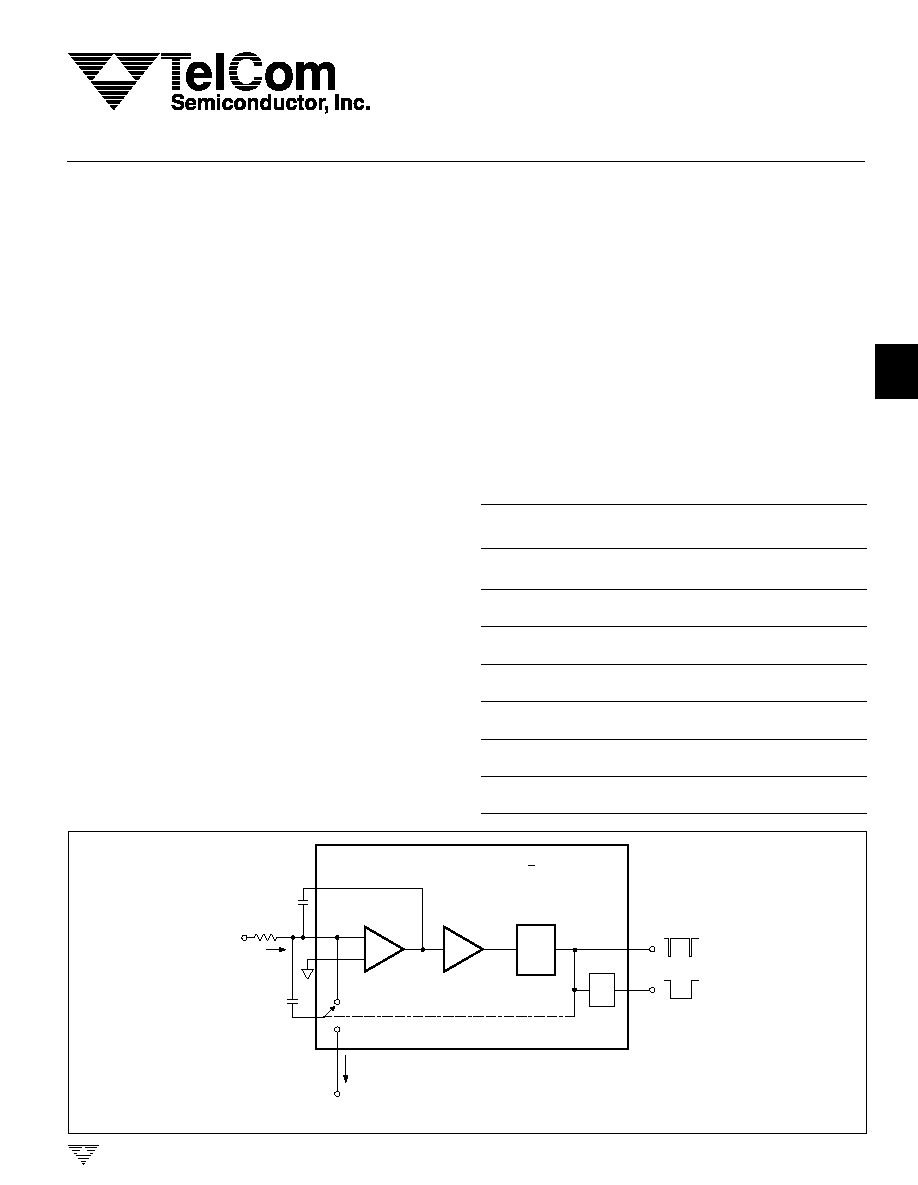
GENERAL DESCRIPTION
The TC9400/TC9401/TC9402 are low-cost voltage-to-
frequency (V/F) converters utilizing low power CMOS
technology. The converters accept a variable analog input
signal and generate an output pulse train whose frequency
is linearly proportional to the input voltage.
The devices can also be used as highly-accurate fre-
quency-to-voltage (F/V) converters, accepting virtually any
input frequency waveform and providing a linearly-propor-
tional voltage output.
A complete V/F or F/V system only requires the addition
of two capacitors, three resistors, and reference voltage.
I
IN
I
REF
TC9400
R
IN
Integrator
OpAmp
Integrator
Capacitor
Threshold
Detector
One
Shot
Pulse Output
Pulse/2 Output
˜
2
Input
Voltage
Reference
Capacitor
Reference
Voltage
ORDERING INFORMATION
Linearity
Temperature
Part No.
(V/F)
Package
Range
TC9400COD
0.05%
14-Pin
0
∞
C to +70
∞
C
SOIC (Narrow)
TC9400CPD
0.05%
14-Pin
0
∞
C to +70
∞
C
Plastic DIP
TC9400EJD
0.05%
14-Pin
≠ 40
∞
C to +85
∞
C
CerDIP
TC9401CPD
0.01%
14-Pin
0
∞
C to +70
∞
C
Plastic DIP
TC9401EJD
0.01%
14-Pin
≠ 40
∞
C to +85
∞
C
CerDIP
TC9402CPD
0.25%
14-Pin
0
∞
C to +70
∞
C
Plastic DIP
TC9402EJD
0.25%
14-Pin
≠ 40
∞
C to +85
∞
C
CerDIP
FUNCTIONAL BLOCK DIAGRAM
TC9400/1/2-5 11/6/96

3-288
TELCOM SEMICONDUCTOR, INC.
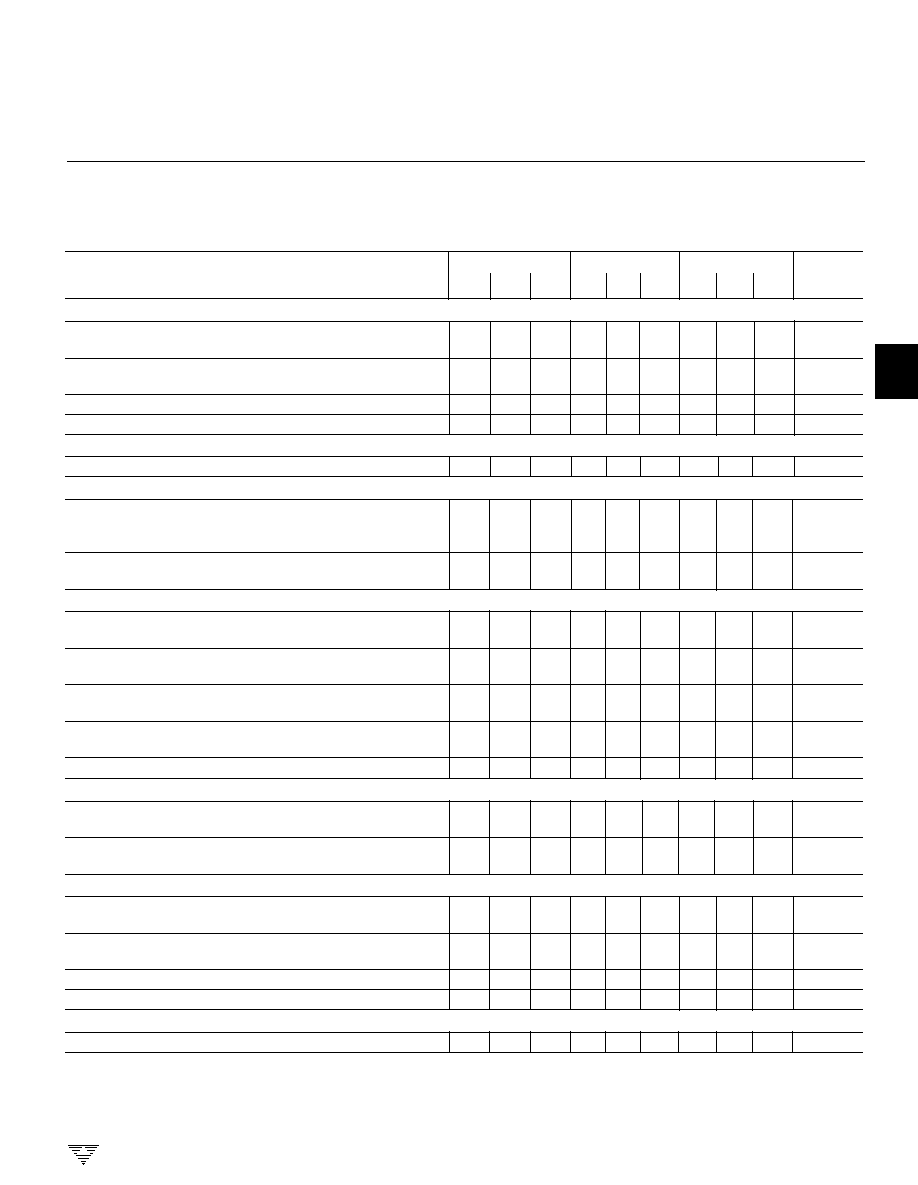
ELECTRICAL CHARACTERISTICS:
V
DD
= +5V, V
SS
= ≠ 5V, V
GND
= 0V, V
REF
= ≠ 5V, R
BIAS
= 100k
,
Full Scale = 10kHz, unless otherwise specified. T
A
= +25
∞
C, unless temperature range is specified (≠ 40
∞
C to +85
∞
C
for E device, 0
∞
C to +70
∞
C for C device).
VOLTAGE-TO-FREQUENCY
TC9401
TC9400
TC9402
Parameter
Definition
Min Typ Max Min Typ Max Min Typ Max
Unit
Accuracy
Linearity 10 kHz
Output Deviation From Straight
--
0.004 0.01
--
0.01 0.05
-- 0.05
0.25
% Full
Line Between Normalized Zero
Scale
and Full-Scale Input
Linearity 100 kHz
Output Deviation From Straight
--
0.04
0.08
--
0.1
0.25
-- 0.25
0.5
% Full
Line Between Normalized Zero
Scale
Reading and Full-Scale Input
Gain Temperature
Variation in Gain A Due to
--
±
25
±
40
--
±
25
±
40
--
±
50
±
100
ppm/
∞
C
Drift (Note 1)
Temperature Change
Full Scale
Gain Variance
Variation From Ideal Accuracy
--
±
10
≠
--
±
10
--
--
±
10
≠
% of
Nominal
Zero Offset (Note 2)
Correction at Zero Adjust for Zero
--
±
10
±
50
--
±
10
±
50
--
±
20
±
100
mV
Output When Input is Zero
Zero Temperature
Variation in Zero Offset Due to
--
±
25
±
50
--
±
25
±
50
--
±
50
±
100
µ
V/
∞
C
Drift (Note 1)
Temperature Change
Analog Input
I
IN
Full Scale
Full-Scale Analog Input Current to
--
10
--
--
10
--
10
--
µ
A
Achieve Specified Accuracy
I
IN
Overrange
Overrange Current
--
--
50
--
--
50
--
--
50
µ
A
Response Time
Settling Time to 0.1% Full Scale
--
2
--
--
2
--
--
2
--
Cycle
Digital Section
V
SAT
@ I
OL
= 10mA
Logic "0" Output Voltage (Note 3)
--
0.2
0.4
--
0.2
0.4
--
0.2
0.4
V
V
OUT
Max ≠ V
OUT
Voltage Range Between Output
--
--
18
--
--
18
--
--
18
V
Common (Note 4)
and Common
Pulse Frequency
--
3
--
--
3
--
--
3
--
µ
sec
Output Width
ABSOLUTE MAXIMUM RATINGS*
V
DD
≠ V
SS
................................................................. +18V
I
IN
...........................................................................10mA
V
OUT
Max ≠V
OUT
Common .......................................... 23V
V
REF
≠ V
SS
.............................................................. ≠ 1.5V
Storage Temperature Range ................ ≠ 65
∞
C to +150
∞
C
Operating Temperature Range
C Device ................................................ 0
∞
C to +70
∞
C
E Device ........................................... ≠ 40
∞
C to +85
∞
C
Package Dissipation (T
A
70
∞
C)
8-Pin CerDIP .................................................. 800mW
8-Pin Plastic DIP ............................................. 730mW
8-Pin SOIC ..................................................... 470mW
Lead Temperature (Soldering, 10 sec) ................. +300
∞
C
*Static-sensitive device. Unused devices must be stored in conductive
material. Protect devices from static discharge and static fields. Stresses
above those listed under Absolute Maximum Ratings may cause perma-
nent damage to the device. These are stress ratings only and functional
operation of the device at these or any other conditions above those
indicated in the operational sections of the specifications is not implied.
Exposure to Absolute Maximum Rating Conditions for extended periods
may affect device reliability.
VOLTAGE-TO-FREQUENCY/
FREQUENCY-TO-VOLTAGE CONVERTERS
TC9400
TC9401
TC9402
3-289
TELCOM SEMICONDUCTOR, INC.
7
6
5
4
3
1
2
8
NOTES: 1. Full temperature range. Guaranteed, Not Tested.
2. I
IN
= 0.
3. Full temperature range, I
OUT
= 10mA.
4. I
OUT
= 10
µ
A.
5. Threshold Detect = 5V, Amp Out = 0V, Full Temperature
Range
ELECTRICAL CHARACTERISTICS: (Cont.)
V
DD
= +5V, V
SS
= ≠ 5V, V
GND
= 0, V
REF
= ≠ 5V, R
BIAS
= 100k
,
Full Scale = 10kHz, unless otherwise specified. T
A
= +25
∞
C, unless temperature range is specified ≠ 40
∞
C to +85
∞
C for
E device, 0
∞
C to +70
∞
C for C device.
FREQUENCY-TO-VOLTAGE
TC9401
TC9400
TC9402
Parameter
Definition
Min
Typ Max Min Typ Max Min Typ Max
Unit
Supply Current
I
DD
Quiescent
Current Required From Positive
(Note 5)
Supply During Operation
--
1.5
6
--
1.5
6
--
3
10
mA
I
SS
Quiescent
Current Required From Negative
(Note 5)
Supply During Operation
--
≠ 1.5
≠ 6
--
≠ 1.5
≠ 6
≠ 3
≠ 10
mA
V
DD
Supply
Operating Range of Positive Supply
4
--
7.5
4
--
7.5
4
--
7.5
V
V
SS
Supply
Operating Range of Negative Supply
≠ 4
--
≠ 7.5 ≠ 4
--
≠ 7.5
≠ 4
--
≠ 7.5
V
Reference Voltage
V
REF
≠V
SS
Range of Voltage Reference Input
≠ 2.5
--
--
≠ 2.5
--
--
≠ 2.5 --
--
V
Accuracy
Nonlinearity (Note 10)
Deviation From Ideal Transfer
--
0.01
0.02
--
0.02 0.05
-- 0.05
0.25
% Full
Function as a Percentage
Scale
Full-Scale Voltage
Input Frequency
Frequency Range for Specified
10
--
100k
10
--
100k
10
--
100k
Hz
Range (Note 7 and 8)
Nonlinearity
Frequency Input
Positive Excursion
Voltage Required to Turn
0.4
--
V
DD
0.4
--
V
DD
0.4
--
V
DD
V
Threshold Detector On
Negative Excursion
Voltage Required to Turn
≠ 0.4
≠ 2 ≠ 0.4
--
≠ 2
≠ 0.4 --
≠ 2
V
Threshold Detector Off
Minimum Positive
Time Between Threshold
--
5
--
--
5
--
--
5
--
µ
sec
Pulse Width (Note 8)
Crossings
Minimum Negative
Time Between Threshold
--
0.5
--
--
0.5
--
--
0.5
µ
sec
Pulse Width (Note 8)
Crossings
Input Impedance
--
10
--
--
10
--
--
10
--
M
Analog Outputs
Output Voltage
Voltage Range of Op Amp Output
--
V
DD
≠ 1
--
--
V
DD
≠ 1
--
-- V
DD
≠ 1
--
V
(Note 9)
for Specified Nonlinearity
Output Loading
Resistive Loading at Output of
2
--
--
2
--
--
2
--
--
k
Op Amp
Supply Current
I
DD
Quiescent
Current Required From Positive
(Note 10)
Supply During Operation
--
1.5
6
--
1.5
6
--
3
10
mA
I
SS
Quiescent
Current Required From Negative
(Note 10)
Supply During Operation
--
≠ 1.5
≠ 6
≠ 1.5 ≠ 6
≠ 3
≠ 10
mA
V
DD
Supply
Operating Range of Positive Supply
4
--
7.5
4
--
7.5
4
--
7.5
V
V
SS
Supply
Operating Range of Negative Supply
≠ 4
--
≠ 7.5 ≠ 4
--
≠ 7.5
≠ 4
--
≠ 7.5
V
Reference Voltage
V
REF
≠V
SS
Range of Voltage Reference Input
≠ 2.5
--
--
≠ 2.5
--
--
≠ 2.5 --
--
V
6. 10Hz to 100kHz.; Guaranteed, Not Tested
7. 5
µ
sec minimum positive pulse width and 0.5
µ
sec minimum
negative pulse width.
8. t
R
= t
F
= 20 nsec.
9. R
L
2k
.; Tested @ 10k
10. Full temperature range, V
IN
= ≠ 0.1V.
VOLTAGE-TO-FREQUENCY/
FREQUENCY-TO-VOLTAGE CONVERTERS
TC9400
TC9401
TC9402

3-290
TELCOM SEMICONDUCTOR, INC.
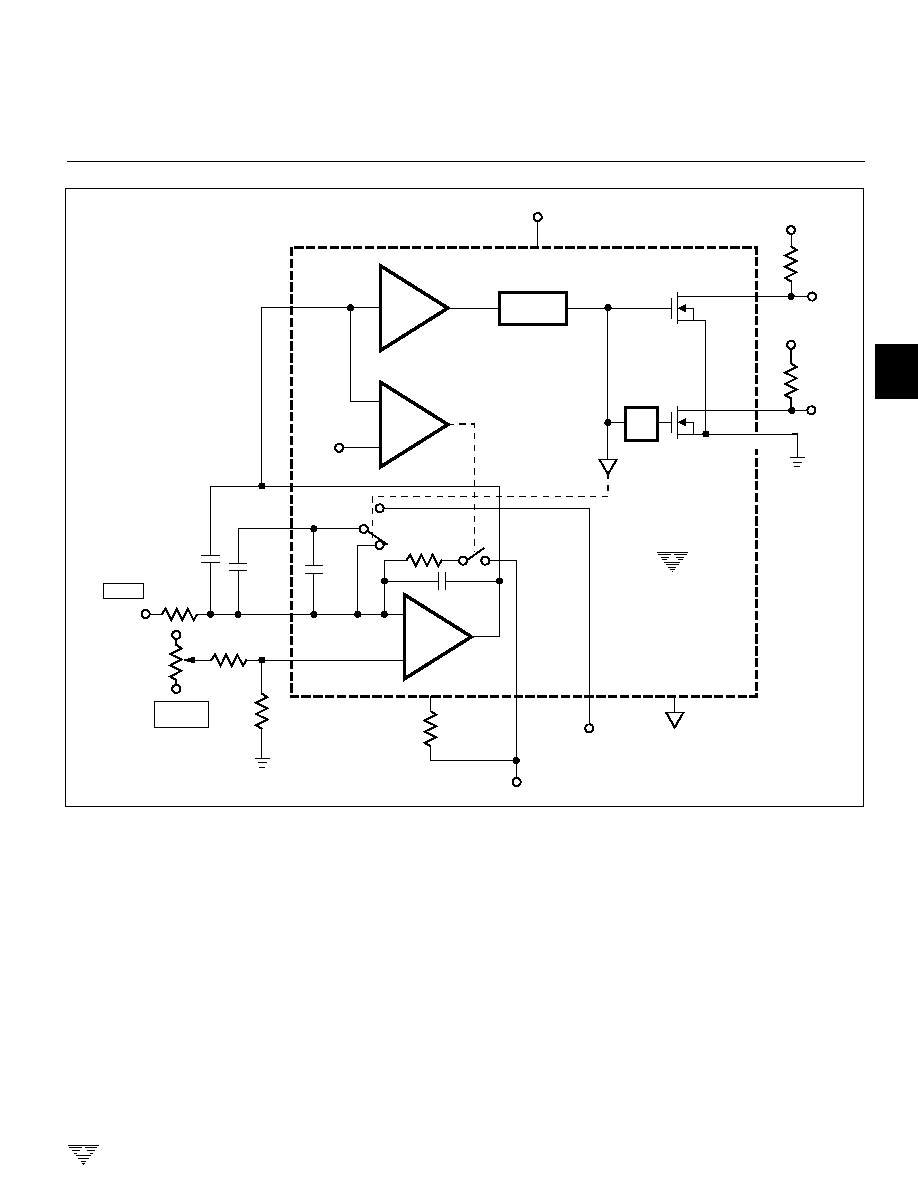
Pin No.
Symbol
Description
1
I
BIAS
This pin sets bias current in the TC9400. Connect to V
SS
through a 100 k
resistor.
See text.
2
Zero Adj
Low frequency adjustment input. See text.
3
I
IN
Input current connection for the V/F converter.
4
V
SS
Negative power supply voltage connection, typically ≠ 5V.
5
V
REF
OUT
Reference capacitor connection.
6
GND
Analog ground.
7
V
REF
Voltage reference input, typically ≠ 5V.
8
Pulse Freq Out
Frequency output. This open drain output will pulse LOW each time the Freq
threshold detector limit is reached. The pulse rate is proportional to input voltage.
9
Output Common
Source connection for the open drain output FETs. See text.
10
Freq/2 Out
This open drain output is a square wave at one half the frequency of the pulse
output (pin 8). Output transitions of this pin occur on the rising edge of pin 8.
11
Threshold Detect
Input to the threshold detector. This pin is the frequency input during F/V operation.
12
Amplifier Out
Output of the integrator amplifier.
13
NC
No internal connection
14
V
DD
Positive power supply connection, typically +5V.
PIN DESCRIPTIONS
PIN CONFIGURATIONS
1
2
3
4
5
6
7
14
13
12
11
10
9
8
VDD
NC
AMPLIFIER OUT
THRESHOLD DETECTOR
FREQ/2 OUT
OUTPUT COMMON
PULSE FREQ OUT
IBIAS
ZERO ADJ
IIN
VSS
VREF OUT
GND
VREF
1
2
3
4
5
6
7
14
13
12
11
10
9
8
VDD
NC
AMPLIFIER OUT
THRESHOLD DETECTOR
FREQ/2 OUT
OUTPUT COMMON
PULSE FREQ OUT
IBIAS
ZERO ADJ
I
IN
V
SS
V
REF
OUT
GND
V
REF
TC9400
TC9401
TC9402
TC9400
TC9401
TC9402
NC = NO INTERNAL CONNECTION
14-Pin Plastic DIP/CerDIP
14-Pin SOIC (Narrow)
VOLTAGE-TO-FREQUENCY/
FREQUENCY-TO-VOLTAGE CONVERTERS
TC9400
TC9401
TC9402
3-291
TELCOM SEMICONDUCTOR, INC.
7
6
5
4
3
1
2
8
Figure 1. 10 Hz to 10 kHz V/F Converter
≠
+
+5V
+5V
14
V
DD
+5V
RL
10k
RL
10k
8
10
9
fOUT
fOUT/2
11
3
µ
sec
DELAY
SELF-
START
12
5
20k
60pF
OpAmp
CINT
820pF
CREF
180pF
12pF
RIN
1M
VIN
INPUT
+5V
≠5V
50k
510k
10k
3
1
OFFSET
ADJUST
IIN
ZERO
ADJUST
0V ≠10V
IBIAS
VSS
4
≠5V
2
OUTPUT
COMMON
VREF OUT
RBIAS
100k
AMP OUT
TC9400
TC9401
TC9402
GND
6
THRESHOLD
DETECTOR
THRESHOLD
DETECT
REFERENCE
VOLTAGE
(TYPICALLY ≠5V)
˜
2
VREF
7
≠3V
At the end of the charging period, C
REF
is shorted out.
This dissipates the charge stored on the reference capaci-
tor, so that when the output again crosses zero the system
is ready to recycle. In this manner, the continued discharg-
ing of the integrating capacitor by the input is balanced out
by fixed charges from the reference voltage. As the input
voltage is increased, the number of reference pulses re-
quired to maintain balance increases, which causes the
output frequency to also increase. Since each charge in-
crement is fixed, the increase in frequency with voltage is
linear. In addition, the accuracy of the output pulse width
does not directly affect the linearity of the V/F. The pulse
must simply be long enough for full charge transfer to take
place.
VOLTAGE-TO-FREQUENCY (V/F)
CIRCUIT DESCRIPTION
The TC9400 V/F converter operates on the principal
of charge balancing. The operation of the TC9400 is easily
understood by referring to Figure 1. The input voltage (V
IN
)
is converted to a current (I
IN
) by the input resistor. This
current is then converted to a charge on the integrating
capacitor and shows up as a linearly decreasing voltage at
the output of the op amp. The lower limit of the output
swing is set by the threshold detector, which causes the
reference voltage to be applied to the reference capacitor
for a time period long enough to charge the capacitor to
the reference voltage. This action reduces the charge on
the integrating capacitor by a fixed amount (q = C
REF
◊
V
REF
), causing the op amp output to step up a finite
amount.
VOLTAGE-TO-FREQUENCY/
FREQUENCY-TO-VOLTAGE CONVERTERS
TC9400
TC9401
TC9402