 | –≠–ª–µ–∫—Ç—Ä–æ–Ω–Ω—ã–π –∫–æ–º–ø–æ–Ω–µ–Ω—Ç: TCM680 | –°–∫–∞—á–∞—Ç—å:  PDF PDF  ZIP ZIP |
Document Outline
- Return to Contents
- List of Figures
- 1. Test Circuit
- 2. Charge Pump Ö Phase 1
- 3. Charge Pump Ö Phase 2
- 4. Charge Pump Ö Phase 3
- 5. Charge Pump Ö Phase 4
- 6. Positive and Negative Converter
- 7. Paralleling TCM680 for Lower Output Source Resistance
- 8. Split Supply Derived from 3V Battery
- List of Tables
- 1. ROUT vs. C1 ,C2
- 2. VRIPPLE (p-p) vs. C3, C4 (IOUT = 10mA)
- Features
- Applications
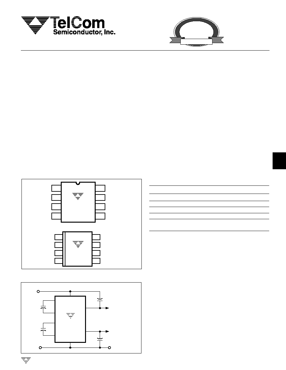
- Pin Configurations (DIP AND SOIC)
- Typical Operating Circuit
- General Description
- Ordering Information
- Absolute Maximum Ratings
- Electrical Characteristics: VIN = +5V, TA = +25∞C, test circuit Figure 1, unless otherwise indicated.
- Pin Description
- Detailed Description
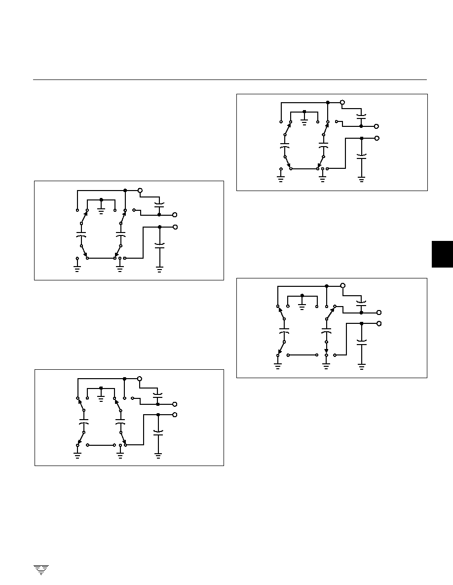
- Phase 1
- Phase 2
- Phase 3
- Phase 4
- Maximum Operating Limits
- Efficiency Considerations
- Applications
- Positive and Negative Converter
- Capacitor Selection
- Paralleling Devices
- ±5V Regulated Supplies From A Single 3V Battery
- Typical Characteristics
4-13
TELCOM SEMICONDUCTOR, INC.
7
6
5
4
3
1
2
8
FEATURES
s
99% Voltage Conversion Efficiency
s
85% Power Conversion Efficiency
s
Wide Voltage Range ......................... +2.0V to +5.5V
s
Only 4 External Capacitors Required
s
Space Saving 8-Pin SOIC Design
APPLICATIONS
s
±
10V From +5V Logic Supply
s
±
6V From a 3V Lithium Cell
s
Handheld Instruments
s
Portable Cellular Phones
s
LCD Display Bias Generator
s
Panel Meters
s
Operational Amplifier Power Supplies
GENERAL DESCRIPTION
The TCM680 is a dual charge pump voltage converter
that develops output voltages of +2V
IN
and ≠ 2V
IN
from a
single input voltage of +2.0V to +5.5V. Common applica-
tions include
±
10V from a single +5V logic supply, and
±
6V
from a +3V lithium battery.
The TCM680 is packaged in a space-saving 8-pin
SOIC package and requires only four inexpensive external
capacitors. The charge pumps are clocked by an on-board
8kHz oscillator. Low output source impedances (typically
150
) provides maximum output currents of 10mA for each
output. Typical power conversion efficiency is 85%.
High efficiency, small installed size and low cost make
the TCM680 suitable for a wide variety of applications that
need both positive and negative power supplies derived
from a single input voltage.
TYPICAL OPERATING CIRCUIT
PIN CONFIGURATIONS (DIP AND SOIC)
C
1
C
1
V
IN
V
OUT
V
OUT
= (≠ 2 x V
IN
)
V
OUT
V
OUT
= ( 2 x V
IN
)
GND
GND
GND
TCM680
4.7
µ
F
4.7
µ
F
C4
C3
C1
4.7
µ
F
2.0V<V
IN
< +5.5V
C2
4.7
µ
F
+5V
C
2
C
2
+
+
+
+
+
+
≠
≠
≠
≠
+
+
1
2
3
4
8
7
6
5
C
1
V
OUT
V
OUT
V
OUT
V
OUT
V
IN
GND
C
1
≠
V
IN
GND
TCM680CPA
TCM680EPA
1
8
2
7
3
6
4
5
TCM680COA
TCM680EOA
+
+
≠
≠
C
1
+
C
2
+
C
1
+
C
2
+
C
2
≠
≠
C
2
≠
ORDERING INFORMATION
Part No.
Package
Temperature
TCM680COA
8-Pin SOIC
0
∞
C to +70
∞
C
TCM680CPA
8-Pin Plastic DIP
0
∞
C to +70
∞
C
TCM680EOA
8-Pin SOIC
≠ 40
∞
C to +85
∞
C
TCM680EPA
8-Pin Plastic DIP
≠ 40
∞
C to +85
∞
C
TC7660EV
Charge Pump Family
Evaluation Kit
+5V TO
±
10V VOLTAGE CONVERTER
TCM680
EVALUATION
KIT
AVAILABLE
TC660-2 9/4/96
4-14
TELCOM SEMICONDUCTOR, INC.
TCM680
+5V TO
±
10V VOLTAGE CONVERTER
ABSOLUTE MAXIMUM RATINGS*
V
IN .....................................................................................................
+6.0V
V
+
OUT ..............................................................................................
+12.0V
V
≠
OUT .............................................................................................
≠ 12.0V
V
≠
OUT
Short-Circuit Duration ............................ Continuous
V
+
OUT
Current ............................................................ 75mA
V
IN
dV/dT .............................................................. 1V/
µ
sec
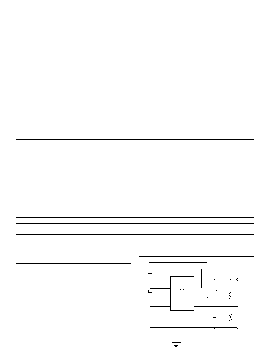
Figure 1. Test Circuit
ELECTRICAL CHARACTERISTICS:
V
IN
= +5V, T
A
= +25
∞
C, test circuit Figure 1, unless otherwise indicated.
Symbol
Parameter
Test Conditions
Min
Typ
Max
Unit
Supply Voltage Range
MIN.
T
A
MAX., R
L
= 2k
2.0
1.5 to 5.5
5.5
V
Supply Current
V
IN
= 3V, R
L
=
--
0.5
1
mA
V
IN
= 5V, R
L
=
--
1
2
V
IN
= 5V, 0
∞
C
T
A
+70
∞
C, R
L
=
--
--
2.5
V
IN
= 5V, ≠ 40
∞
C
T
A
+85
∞
C, R
L
=
--
--
3
Negative Charge Pump Output
I
L
≠
= 10mA, I
L
+
= 0mA, V
IN
= 5V
--
140
180
Source Resistance
I
L
≠
= 5mA, I
L
+
= 0mA, V
IN
= 2.8V
--
180
250
I
L
≠
= 10mA, I
L
+
= 0mA, V
IN
= 5V:
0
∞
C
T
A
+70
∞
C
--
--
220
≠ 40
∞
C
T
A
+85
∞
C
--
--
250
Positive Charge Pump Output
I
L
+
= 10mA, I
L
≠
= 0mA, V
IN
= 5V
--
140
180
Source Resistance
I
L
+
= 5mA, I
L
≠
= 0mA, V
IN
= 2.8V
--
180
250
I
L
+
= 10mA, I
L
≠
= 0mA, V
IN
= 5V:
0
∞
C
T
A
+70
∞
C
--
--
220
≠ 40
∞
C
T
A
+85
∞
C
--
--
250
F
OSC
Oscillator Frequency
--
21
--
kHz
P
EFF
Power Efficiency
R
L
= 2k
--
85
--
%
V
OUT
E
FF
Voltage Conversion Efficiency
V
+
OUT
, R
L
=
97
99
--
%
V
≠
OUT
, R
L
=
97
99
--
TelCom Semiconductor reserves the right to make changes in the circuitry or specifications detailed in this manual at any time without notice. Minimums
and maximums are guaranteed. All other specifications are intended as guidelines only. TelCom Semiconductor assumes no responsibility for the use of
any circuits described herein and makes no representations that they are free from patent infringement.
Power Dissipation (T
A
70
∞
C)
Plastic DIP ...................................................... 730mW
Small Outline .................................................. 470mW
Storage Temperature ............................ ≠ 65
∞
C to +150
∞
C
Lead Temperature (Soldering, 10 sec) ................. +300
∞
C
C
1
C
1
C
2
C
3
C
2
V
IN
V
IN
VOUT
VOUT
VOUT
GND
GND
TCM680
4.7
µ
F
4.7
µ
F
10
µ
F
C
4
10
µ
F
8
7
6
5
4
3
2
1
VOUT
C
2
R
L
R
L
C
1
≠
+
≠
≠
+
+
+
≠
+
≠
PIN DESCRIPTION
8-Pin
DIP/SOIC
Symbol
Description
1
C
1
≠
Input. Capacitor C1 negative terminal.
2
C
2
+
Input. Capacitor C2 positive terminal.
3
C
2
≠
Input. Capacitor C2 negative terminal.
4
V
≠
OUT
Output. Negative output voltage (≠2V
IN
).
5
GND
Input. Device ground.
6
V
IN
Input. Power supply voltage.
7
C
1
+
Input. Capacitor C1 positive terminal.
8
V
+
OUT
Output. Positive output voltage (+2V
IN
)
*Stresses above those listed in "Absolute Maximum Ratings" may cause
permanent damage to the device. These are stress ratings only and
functional operation of the device at these or other conditions above those
indicated in the operation section of the specification is not implied.
Exposure to the Absolute Maximum Ratings conditions for extended
periods of time may affect device reliability.
4-15
TELCOM SEMICONDUCTOR, INC.
7
6
5
4
3
1
2
8
TCM680
+5V TO
±
10V VOLTAGE CONVERTER
Figure 4. Charge Pump ≠ Phase 3
Phase 2
V
SS
transfer ≠ Phase two of the clock connects the
negative terminal of C
2
to the V
SS
storage capacitor C
3
and
the positive terminal of C
2
to ground, transferring the gener-
ated ≠10V to C
3
. Simultaneously, the positive side of capaci-
tor C
1
is switched to +5V and the negative side is connected
to ground.
Phase 3
V
DD
charge storage ≠ The third phase of the clock is
identical to the first phase ≠ the charge transferred in C
1
produces ≠5V in the negative terminal of C
1
, which is applied
to the negative side of capacitor C
2
. Since C
2
+
is at +5V, the
voltage potential across C
2
is 10V.
Figure 3. Charge Pump ≠ Phase 2
DETAILED DESCRIPTION
Phase 1
V
SS
charge storage ≠ The positive side of capacitors C
1
and C
2
are connected to +5V at the start of this phase. C
1
+
is
then switched to ground and the charge in C
1
≠
is transferred
to C
2
≠
. Since C
2
+
is connected to +5V, the voltage potential
across capacitor C
2
is now 10V.
Phase 4
V
DD
transfer ≠ The fourth phase of the clock connects
the negative terminal of C
2
to ground, and transfers the
generated 10V across C
2
to C
4
, the V
DD
storage capacitor.
Again, simultaneously with this, the positive side of capaci-
tor C
1
is switched to +5V and the negative side is connected
to ground, and the cycle begins again.
Figure 2. Charge Pump ≠ Phase 1
V
IN
= +5V
V
SS
V
DD
≠5V
SW4
SW1
SW2
SW3
C
2
C
4
C
3
C
1
+
≠
+
+
≠
≠
+
≠
+5V
V
SS
V
DD
≠10V
SW4
SW2
SW1
SW3
C
2
C
3
C
1
+
≠
+
+
≠
≠
C
4
+
≠
V
IN
= +5V
V
SS
V
DD
≠5V
SW4
SW1
SW2
SW3
C
2
C
4
C
3
C
1
+
≠
+
+
≠
≠
+
≠
Figure 5. Charge Pump ≠ Phase 4
+5V
V
SS
V
DD
≠10V
SW4
SW2
SW1
SW3
C
2
C
3
C
1
+
≠
+
+
≠
≠
C
4
+
≠
MAXIMUM OPERATING LIMITS
The TCM680 has on-chip zener diodes that clamp V
IN
to 5.8V, V
+
OUT
to 11.6V, and V
≠
OUT
to ≠11.6V. Never exceed
the maximum supply voltage or excessive current will be
shunted by these diodes, potentially damaging the chip. The
TCM680 will operate over the entire operating temperature
range with an input voltage of 2V to 5.5V.
4-16
TELCOM SEMICONDUCTOR, INC.
TCM680
+5V TO
±
10V VOLTAGE CONVERTER
EFFICIENCY CONSIDERATIONS
Theoretically a charge pump can approach 100% effi-
ciency under the following conditions:
∑ The charge Pump switches have virtually no offset
and extremely low on resistance
∑ Minimal power is consumed by the drive circuitry
∑ The impedances of the reservoir and pump capaci-
tors are negligible
For the TCM680, efficiency is as shown below:
Efficiency V
+
= V
DD
/(2V
IN
)
V
DD
= 2V
IN
≠ V
+
DROP
V
+
DROP
= (I
+
OUT
)(R
+
OUT
)
Efficiency V
≠
= V
SS
/(≠ 2V
IN
)
V
SS
= 2V
IN
≠ V
≠
DROP
V
≠
DROP
= (I
≠
OUT
)(R
≠
OUT
)
Power Loss
= (V
+
DROP
)(I
+
OUT
) + (V
≠
DROP
)(I
≠
OUT
)
There will be a substantial voltage difference between
(V
+
OUT
≠ V
IN
) and V
IN
for the positive pump and between
V
+
OUT
and V
≠
OUT
if the impedances of the pump capacitors C
1
and C
2
are high with respect to the output loads.
Larger values of reservoir capacitors C
3
and C
4
will
reduce output ripple. Larger values of both pump and
reservoir capacitors improve the efficiency. See "Capacitor
Selection" in Applications Section.
APPLICATIONS
Positive and negative Converter
The most common application of the TCM680 is as a
dual charge pump voltage converter which provides positive
and negative outputs of two times a positive input voltage.
The simple circuit of Figure 6 performs this same function
using the TCM680 and external capacitors, C
1
, C
2
, C
3
and C
4.
Figure 6. Positive and Negative Converter
C
1
C
1
C
2
C
3
C
2
V
IN
V
IN
V
OUT
V
OUT
V
OUT
GND
GND
TCM680
22
µ
F
22
µ
F
22
µ
F
C
4
22
µ
F
8
7
6
5
4
3
2
1
V
OUT
C
2
C
1
+
+
≠
+
≠
≠
+
≠
Capacitor Selection
The TCM680 requires only 4 external capacitors for
operation. These can be inexpensive polarized aluminum
electrolytic types. For the circuit in Figure 6 the output
characteristics are largely determined by the external
capacitors. An expression for R
OUT
can be derived as shown
below:
R
+
OUT
= 4(R
SW1
+ R
SW2
+ ESR
C1
+ R
SW3
+ R
SW4
+ ESR
C2
)
+4(R
SW1
+ R
SW2
+ ESR
C1
+ R
SW3
+ R
SW4
+ ESR
C2
)
+1/(f
PUMP
x C1) + 1/(f
PUMP
x C2) + ESR
C4
R
≠
OUT
= 4(R
SW1
+ R
SW2
+ ESR
C1
+ R
SW3
+ R
SW4
+ ESR
C2
)
+4(R
SW1
+ R
SW2
+ ESR
C1
+ R
SW3
+ R
SW4
+ ESR
C2
)
+1/(f
PUMP
x C1) + 1/(f
PUMP
x C2) + ESR
C3
Assuming all switch resistances are approximately
equal...
R
+
OUT
= 32R
SW
+ 8ESR
C1
+ 8ESR
C2
+ ESR
C4
+1/(f
PUMP
x C1) + 1/(f
PUMP
x C2)
R
≠
OUT
= 32R
SW
+ 8ESR
C1
+ 8ESR
C2
+ ESR
C3
+1/(f
PUMP
x C1) + 1/(f
PUMP
x C2)
R
OUT
is typically 140
at +25
∞
C with V
IN
= +5V and C1
and C2 as 4.7
µ
F low ESR capacitors. The fixed term
(32R
SW
) is about 130
. It can be seen easily that increasing
or decreasing values of C1 and C2 will affect efficiency by
changing R
OUT
. However, be careful about ESR. This term
can quickly become dominant with large electrolytic capaci-
tors. Table 1 shows R
OUT
for various values of C1 and C2
(assume 0.5
ESR). C1 and C4 must be rated at 6VDC or
greater while C2 and C3 must be rated at 12VDC or greater.
Output voltage ripple is affected by C3 and C4. Typically
the larger the value of C3 and C4 the less the ripple for a
given load current. The formula for V
RIPPLE(p-p)
is given
below:
V
+RIPPLE(p-p)
= {1/[2(f
PUMP
/3) x C4] + 2(ESR
C4
)}(I
+
OUT
)
V
≠RIPPLE(p-p)
= {1/[2(f
PUMP
/3) x C3] + 2(ESR
C3
)}(I
≠
OUT
)
For a 10
µ
F (0.5
ESR) capacitor for C3, C4,
f
PUMP
= 21kHz and I
OUT
= 10mA the peak-to-peak ripple
voltage at the output will be less than 100mV. In most
applications (I
OUT
< = 10mA) 10-20
µ
F output capacitors and
1-5
µ
F pump capacitors will suffice. Table 2 shows V
RIPPLE
for different values of C3 and C4 (assume 1
ESR).
4-17
TELCOM SEMICONDUCTOR, INC.
7
6
5
4
3
1
2
8
TCM680
+5V TO
±
10V VOLTAGE CONVERTER
Table 1. R
OUT
vs. C1 ,C2
C1, C2 (
µ
F)
R
OUT
(
)
0.1
1089
0.47
339
1
232
3.3
165
4.7
157
10
146
22
141
100
137
Table 2. V
RIPPLE (p-p)
vs. C3, C4 (I
OUT
= 10mA)
C3, C4 (
µ
F)
V
RIPPLE
(mV)
0.47
1540
1
734
3.3
236
4.7
172
10
91
22
52
100
27
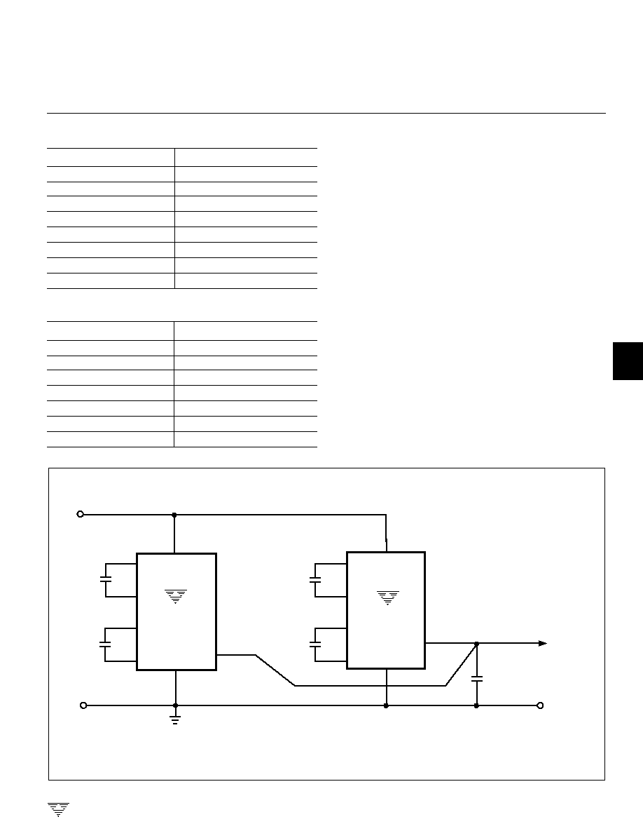
Paralleling Devices
Paralleling multiple TCM680s reduces the output resis-
tance of both the positive and negative converters. The
effective output resistance is the output resistance of a
single device divided by the number of devices. As illus-
trated in Figure 7, each requires separate pump capacitors
C
1
and C
2
, but all can share a single set of reservoir
capacitors.
±
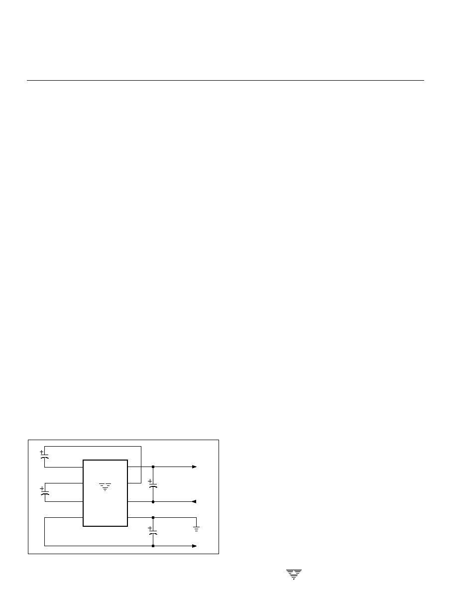
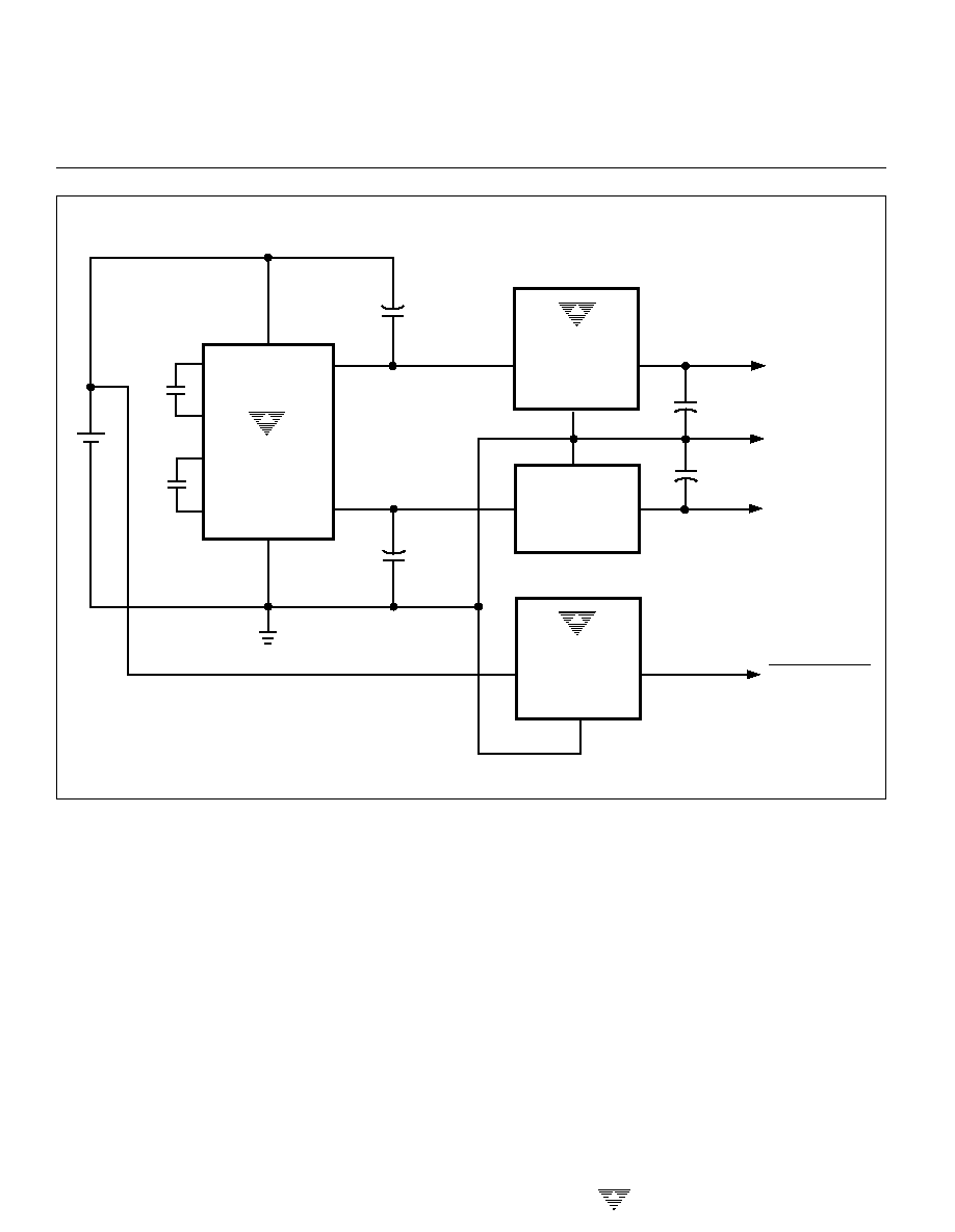
5V Regulated Supplies From A Single
3V Battery
Figure 8 shows a complete
±
5V power supply using one
3V battery. The TCM680 provides +6V at V
+
OUT
, which is
regulated to +5V by the TC55, and ≠5V by the negative LDO.
The input to the TCM680 can vary from 3V to 6V without
affecting regulation appreciably. With higher input voltage,
more current can be drawn from the outputs of the TCM680.
With 5V at V
IN
, 10mA can be drawn from both regulated
outputs simultaneously. Assuming 150
source resistance
for both converters, with (I
+
L
+ I
L
) = 20mA, the positive charge
pump will droop 3V, providing +7V for the negative charge
pump.
C
1
C
2
V
OUT
V
OUT
C
OUT
V
IN
V
IN
V
IN
GND
GND
10
µ
F
10
µ
F
22
µ
F
10
µ
F
10
µ
F
NEGATIVE
SUPPLY
TCM680
C
2
C
1
C
2
C
1
C
1
C
2
TCM680
GND
+
≠
+
≠
+
≠
+
≠
+
≠
+
+
≠
≠
+
≠
≠
≠
≠
+
≠
Figure 7. Paralleling TCM680 for Lower Output Source Resistance
4-18
TELCOM SEMICONDUCTOR, INC.
Figure 8. Split Supply Derived from 3V Battery
C
1
C
1
≠
V
IN
V
SS
V
IN
V
OUT
V
SS
V
IN
V
OUT
GND
TCM680
3V
C
2
C
2
≠
TC55RP5002Exx
V
SS
V
IN
V
OUT
GROUND
+5 SUPPLY
≠5 SUPPLY
LOW BATTERY
NEGATIVE LDO
TC54VC2702Exx
V
OUT
V
OUT
C
OUT
1
µ
F
+6V
≠6V
1
µ
F
C
OUT
+
+
≠
+
≠
+
≠
+
≠
≠
+
≠
+
≠
+
+
≠
+
+
≠
22
µ
F
22
µ
F
10
µ
F
10
µ
F
TCM680
+5V TO
±
10V VOLTAGE CONVERTER
4-19
TELCOM SEMICONDUCTOR, INC.
7
6
5
4
3
1
2
8
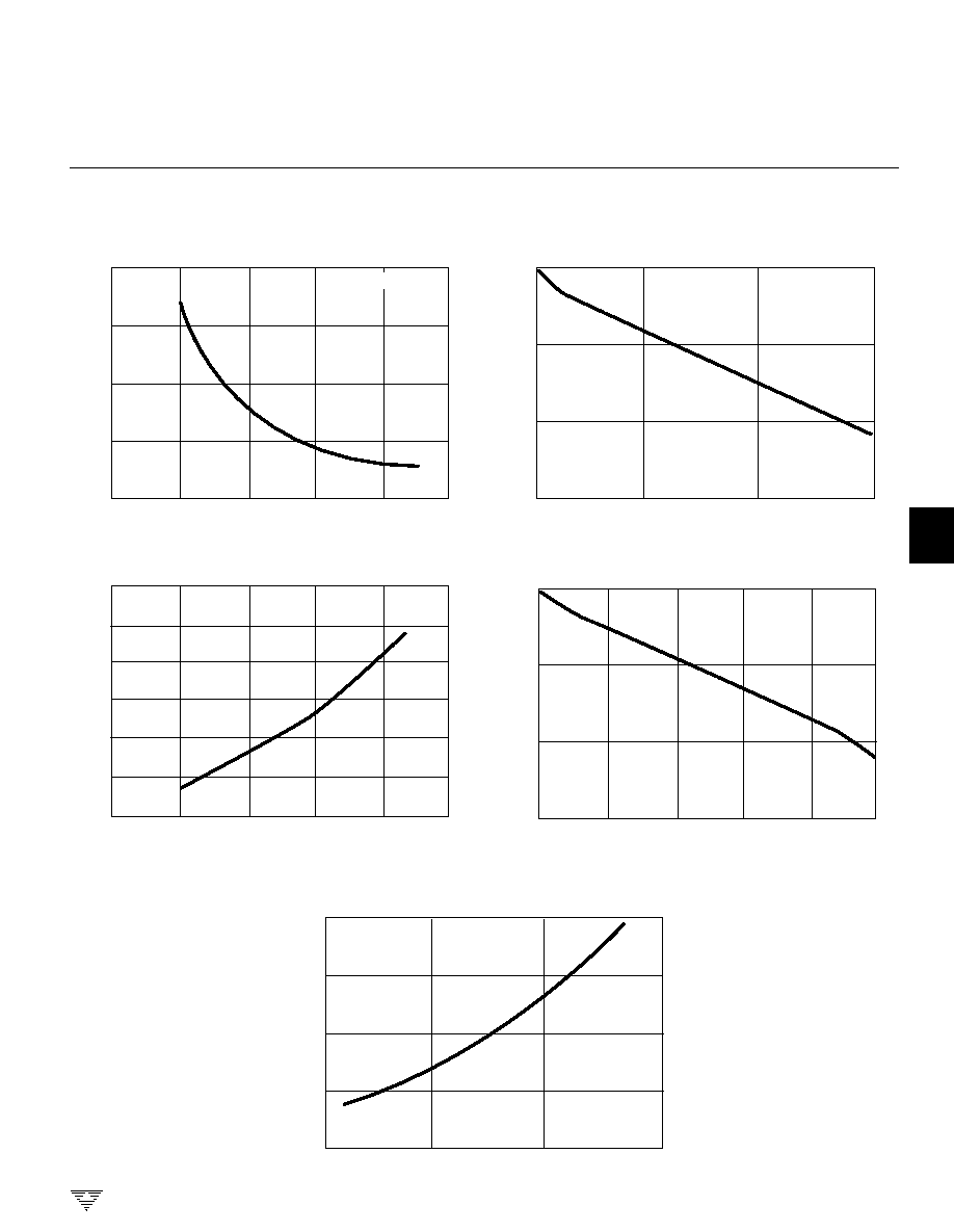
TYPICAL CHARACTERISTICS
1
2
3
4
5
6
VIN (V)
ROUT
ROUT
300
250
200
150
100
OUTPUT RESISTANCE (
)
V
+
OUT
or V
≠
OUT
Output Resistance vs. V
IN
C
1
≠ C
4
= 10
µ
F
-50
0
50
100
TEMPERATURE (
∞
C)
180
160
140
120
100
OUTPUT SOURCE RESISTANCE (
)
Output Source Resistance vs. Temperature
1
2
3
4
5
6
VIN (V)
1.4
1.2
1.0
0.8
0.6
0.4
0.2
SUPPLY CURRENT (mA)
Supply Current vs. V
IN
NO LOAD
0
5
10
15
LOAD CURRENT (mA)
10.0
9.0
8.0
7.0
10.0
9.0
8.0
7.0
V
OUT
(V)
V
OUT
(V)
V
OUT
or V
OUT
vs. Load Current
VIN = 5V
VIN = 5V
+
≠
0
2
4
6
8
10
OUTPUT CURRENT (mA) From VOUT TO VOUT
Output Voltage vs. Output Current From VOUT to VOUT
+
≠
+
≠
VIN = 5V
IOUT = 10mA
TCM680
+5V TO
±
10V VOLTAGE CONVERTER