
CNY21N
TELEFUNKEN Semiconductors
Rev. A1, 11-Jun-96
1 (10)
Optocoupler with Phototransistor Output
Description
The CNY21N consists of a phototransistor optically
coupled to a gallium arsenide infrared emitting diode in
a 4-lead plastic dual inline package.
The single components are mounted on one leadframe in
the opposite position, providing a fixed distance between
input and output for highest safety requirements of
> 3 mm.
Application
Circuits for safe protective separation against electrical
shock according to safety class II (reinforced isolation):
D For application class I - IV at mains voltage
300 V
D For application class I - IV at mains voltage
600 V
D For application class I - III at mains voltage
1000 V
according, to VDE 0884, table 2, suitable for:
Switch-mode power supplies, computer peripheral
interface, microprocessor system interface, line
receiver.
95 10533
These couplers perform safety functions according to the following equipment standards:
D VDE 0884
Optocoupler providing protective separation
D VDE 0804
Telecommunication apparatus and data processing
D VDE 0805/IEC 950/EN 60950
Office machines (applied for reinforced isolation for
mains voltage
400 V
RMS
)
D VDE 0860/lEC 65
Safety for mains operated electronic and related
household apparatus
D VDE 0700/IEC 335
Household equipment
D VDE 0160
Electronic equipment for electrical power installation
D VDE 0750/IEC 601
Medical equipment
Pin Connection
C
E
A (+)
C (�)
95 10850

CNY21N
TELEFUNKEN Semiconductors
Rev. A1, 11-Jun-96
2 (10)
Features
According to VDE 0884
D Rated impulse voltage (transient overvoltage)
V
IOTM
= 8 kV peak
D Isolation test voltage (partial discharge test voltage)
V
pd
= 2.8 kV peak
D Rated isolation voltage (RMS includes DC)
V
IOWM
= 1000 V
RMS
(1450 V peak)
D Rated recurring peak voltage (repetitive)
V
IORM
= 1000 V
RMS
D Creeping current resistance according to
VDE 0303/IEC 112
Comparative Tracking Index: CTI = 275
D Thickness through insulation > 3 mm
D Isolation materials according to UL 94
D Pollution degree 2 (DIN/VDE 0110)
D Climatic classification 55/085/21 (IEC 68 part 1)
D Further approvals: BS 415, BS 7002, SETI: IEC 950,
UL 1577: File no: E 76222
D Special construction: therefore extra low coupling
capacity of typical 0.3 pF, high Common Mode
Rejection
D Low temperature coefficient of CTR
D Current Transfer Ratio (CTR) of typical 60%
Absolute Maximum Ratings
Input (Emitter)
Parameters
Test Conditions
Symbol
Value
Unit
Reverse voltage
V
R
5
V
Forward current
I
F
50
mA
Forward surge current
t
p
10
ms
I
FSM
1.5
A
Power dissipation
T
amb
25
�
C
P
tot
120
mW
Junction temperature
T
j
100
�
C
Output (Detector)
Parameters
Test Conditions
Symbol
Value
Unit
Collector emitter voltage
V
CEO
32
V
Emitter collector voltage
V
ECO
5
V
Collector current
I
C
50
mA
Collector peak current
t
p
/T = 0.5, t
p
10 ms
I
CM
100
mA
Power dissipation
T
amb
25
�
C
P
tot
130
mW
Junction temperature
T
j
100
�
C
Coupler
Parameters
Test Conditions
Symbol
Value
Unit
AC isolation test voltage (RMS)
V
IO
8.2
kV
Total power dissipation
T
amb
25
�
C
P
tot
250
mW
Ambient temperature range
T
amb
�55 to +85
�
C
Storage temperature range
T
stg
�55 to +100
�
C
Soldering temperature
2 mm from case t
10 s
T
sd
260
�
C

CNY21N
TELEFUNKEN Semiconductors
Rev. A1, 11-Jun-96
3 (10)
Maximum Safety Ratings
1)
(according to VDE 0884)
Input (Emitter)
Parameters
Test Conditions
Symbol
Value
Unit
Forward current
I
si
120
mA
Output (Detector)
Parameters
Test Conditions
Symbol
Value
Unit
Power dissipation
T
amb
25
�
C
P
si
250
mW
Coupler
Parameters
Test Conditions
Symbol
Value
Unit
Rated impulse voltage
V
IOTM
8
kV
Safety temperature
T
si
180
�
C
1)
This device is used for protective separation against electrical shock only within the maximum safety ratings.
This must be ensured by using protective circuits in the applications.
Derating Diagram
0
25
50
75
100
125
150
175
200
225
250
0
25
50
75
100 125 150 175 200
mA
( mA
)
T
amb
(
�
C )
95 10888
P
si
(mW)
I
si
(mA)
CNY21N
TELEFUNKEN Semiconductors
Rev. A1, 11-Jun-96
4 (10)
Electrical Characteristics
T
amb
= 25
�
C
Input (Emitter)
Parameters
Test Conditions
Symbol
Min.
Typ.
Max.
Unit
Forward voltage
I
F
= 50 mA
V
F
1.25
1.6
V
Breakdown voltage
I
R
= 100
mA
V
(BR)
5
V
Junction capacitance
V
R
= 0, f = 1 MHz
C
j
50
pF
Output (Detector)
Parameters
Test Conditions
Symbol
Min.
Typ.
Max.
Unit
Collector emitter
breakdown voltage
I
C
= 1 mA
V
(BR)CEO
32
V
Emitter collector
breakdown voltage
I
E
= 100
mA
V
(BR)ECO
5
V
Collector emitter
cut-off current
V
CE
= 20 V, I
f
= 0
I
CEO
200
nA
Coupler
Parameters
Test Conditions
Symbol
Min.
Typ.
Max.
Unit
AC isolation test voltage
(RMS)
f = 50 Hz, t = 1 s
V
IO
8.2
kV
Collector emitter
saturation voltage
I
F
= 10 mA, I
C
= 1 mA
V
CEsat
0.3
V
Cut-off frequency
V
CE
= 5 V, I
F
= 5 mA,
R
L
= 100
W
f
c
170
kHZ
Coupling capacitance
f = 1 MHz
C
k
0.3
pF
I
C
/I
F
I
F
= 10 mA, V
CE
= 5 V
CTR
0.25
0.6
CNY21N
TELEFUNKEN Semiconductors
Rev. A1, 11-Jun-96
5 (10)
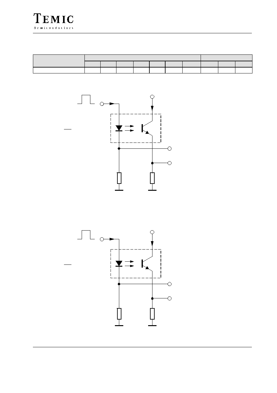
Switching Characteristics (Typical Values)
V
S
= 5 V
Type
R
L
= 100
W (see figure 1)
R
L
= 1 k
W (see figure 2)
yp
t
d
[
ms] t
r
[
ms] t
on
[
ms] t
s
[
ms] t
f
[
ms] t
off
[
ms] I
C
[mA]
t
on
[
ms] t
off
[
ms] I
F
[mA]
CNY21N
2.6
2.4
5.0
0.3
2.7
3.0
5
11
13.5
20
Channel I
Channel II
100
W
50
W
+ 5 V
Oscilloscope
R
L
w 1 MW
C
L
v 20 pF
IC = 5 mA;
IF
I
F
R
G
= 50
W
t
p
t
p
= 50 ms
T
= 0.01
0
95 10900
Adjusted through
input amplitude
Figure 1. Test circuit, non-saturated operation
Channel I
Channel II
1 k
W
50
W
+ 5 V
Oscilloscope
R
L
w 1 MW
C
L
v 20 pF
I
C
I
F
= 20 mA
I
F
R
G
= 50
W
t
p
t
p
= 50
ms
T
= 0.01
0
95 10901
Figure 2. Test circuit, saturated operation