TELEFUNKEN Semiconductors
TDA4481-D
Rev. A1: 23.02.1995
1 (10)
Multistandard quasi parallel-sound processor for
Mono-TV-Sets
Technology: Bipolar
Features
High signal sensitivity
High signal to noise ratio
Easy alignment of the multistandard filters
Converter for different intercarrier frequencies
AF output level matched to SIMAVELEC condition
Few external components
Alignment free AM demodulator for standard L
Standardized SCART interface
Standard-, SCART- and Mute-switch TTL compatible
AF attenuator
ESD protected
Case:
20-pin dual inline plastic
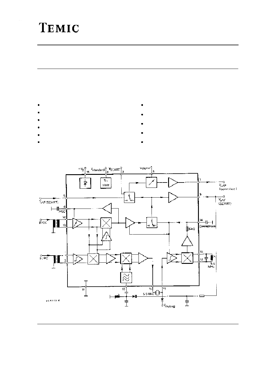
Figure 1 Block diagram
TELEFUNKEN Semiconductors
TDA4481-D
Rev. A1: 23.02.1995
2 (10)
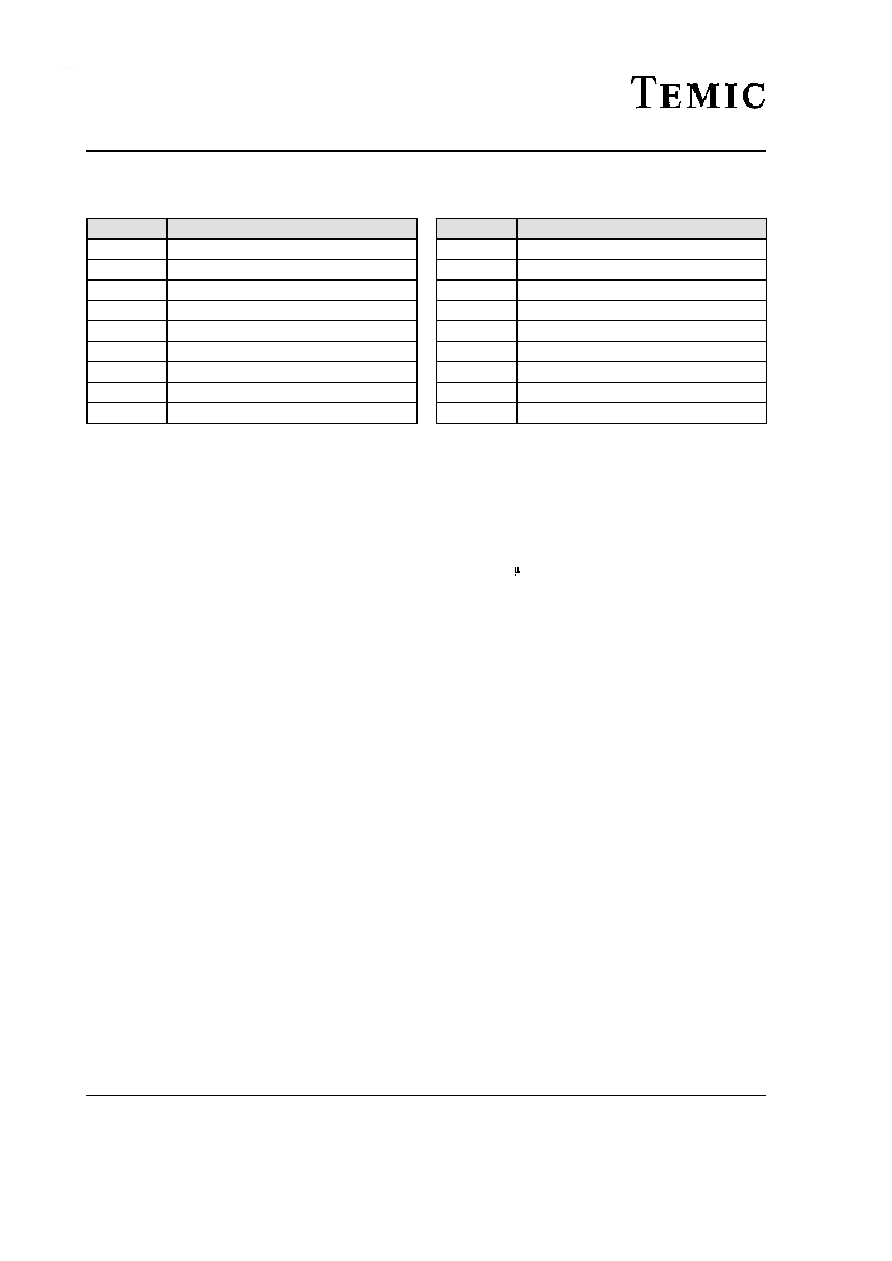
Pin Configuration
Pin
Function
1�2
Picture-IF-carrier input
3
SCART-switch
4
AGC storage capacitor
5
SCART-AF input
6
Standard switch
7
AF output (controlled)
8
Volume control voltage
9
SCART-AF output
10
VC0 tank circuit
Pin
Function
11
Ground
12�13
FM demod. circuit 5.5 MHz
14
FM deemphasis capacitor
15
Intercarrier output 5.5 MHz
16
Supply voltage
17
Intercarrier input 5.5 MHz
and muting
18�19
Sound-IF-carrier input
20
not connected
Description
This circuit configuration permits high-quality processing
of audio carriers for all standards, providing separate inputs
for the video and audio carriers. The audio carrier signal
(FM or AM) is passed to two multiplying mixer
arrangements via a 3-stage variable wide-band amplifier
with levelled output signals. One mixer demodulates AM
and generates the gain control signal. The second mixer
operates as an intercarrier demodulator and supplies the
intermediate AF carrier.
The video carrier signal required to form the intercarrier is
decoupled in a prelimited and selected form from the
demodulator tank of the intermediate video frequency
circuit (TDA 4453 or TDA 4439) and led to the intercarrier
mixer via a limiting amplifier. By virtue of the system, the
Nyquist range of the IF input filter in the video channel
affects the attainable AF signal-to-noise ratio.
The audio FM IF carrier reaches a quadrature demodulator
via an interconnected IF-filter and subsequent limiting
amplifier. The resulting AF signal is led via a low-pass
amplifier with increased level and the AF standard switch
to the SCART switch. It is available at both AF outputs,
regulated (pin
7)
and unregulated (pin 9).
Pin 14 is provided to connect a de-emphasis capacitor
(10 nF for 50 s). The de-emphasis is effective for both AF
outputs during FM operation, but deactivated for AM
operation.
A frequency converter is inserted to mix the different
possible sound frequency standards (4.5, 6.0, 6.5 MHz)
into a uniform intermediate audio frequency, e.g. 5.5 MHz.
The VCO frequency (pin 10) can be controlled from the
unlevelled AF output at pin 9 or the de-emphasis
connection at pin 14.
The intercarrier and converter circuits as well as the FM
demodulator are deactivated during AM modulation. FM
muting is also possible if a switching voltage is applied to
pin 17.
All switching functions (standard, SCART, mute) can take
place with TTL-equivalent level.
TELEFUNKEN Semiconductors
TDA4481-D
Rev. A1: 23.02.1995
3 (10)
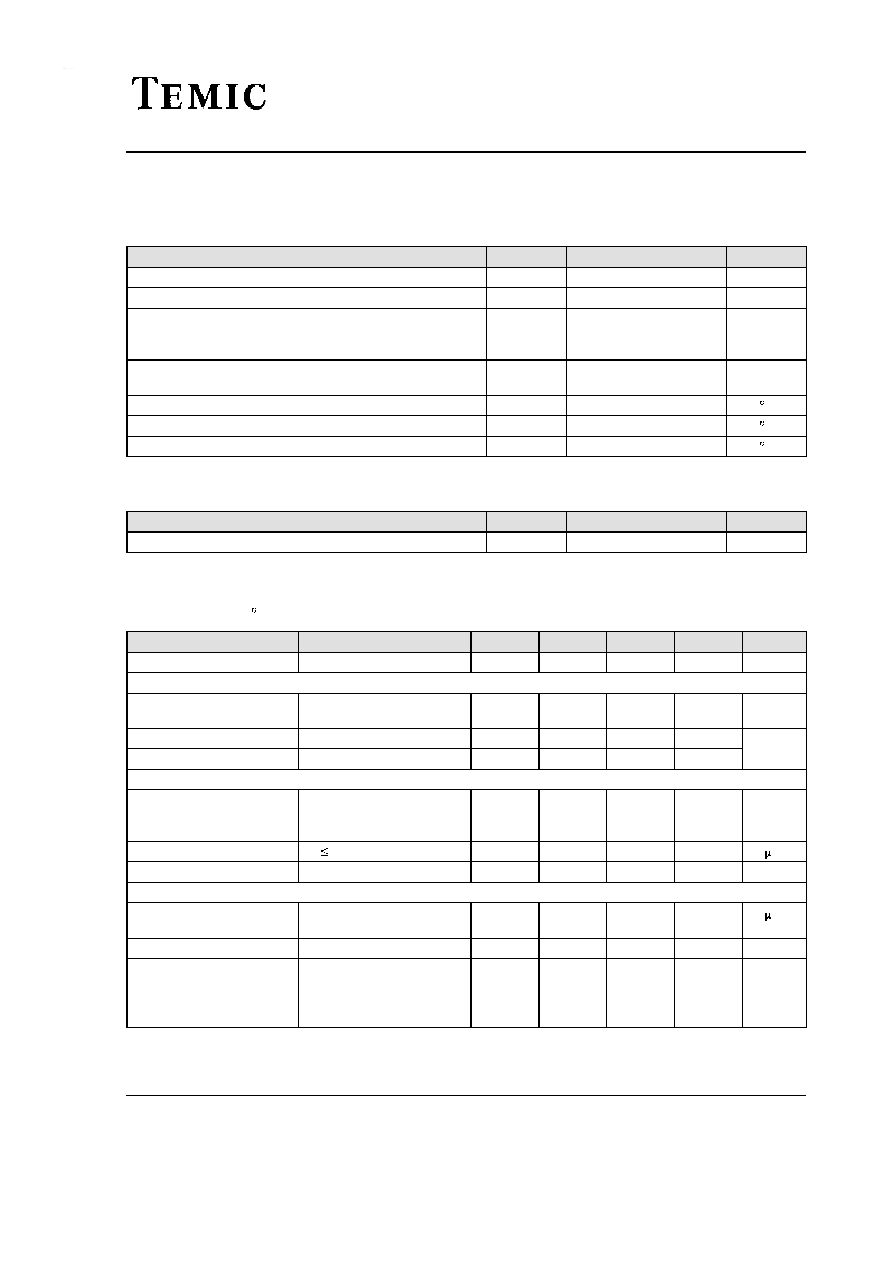
Absolute Maximum Ratings
Reference point Pin 11, unless otherwise specified
Parameters
Symbol
Value
Unit
Supply voltage
Pin 16
V
S
10 ... 13.5
V
Supply current
Pin 16
I
S
80
mA
External voltages
Pin 3,6
Pin 1,2,4,5,7,8,9,12,
13,14,15,16,17,18,19,
V
ext
V
ext
V
5
6
V
V
Power dissipation
(in soldered position)
P
tot
1
W
Junction temperature
T
j
125
C
Ambient temperature range
T
amb
�25 to + 70
C
Storage temperature range
T
stg
�25 to +125
C
Thermal Resistance
Parameters
Symbol
Value
Unit
Junction ambient
R
thJA
60
K/W
Electrical Characteristics
V
S
= 12 V, T
amb
= 25 C, reference point Pin 20 (11), unless otherwise specified
Parameters
Test Conditions / Pins
Symbol
Min.
Typ.
Max.
Unit
Supply voltage range
Pin 16
V
S
10
13.5
V
Supply current
FM-operation
AM-operation
Pin 16
Pin 16
I
S
65
55
mA
Input DC voltage
Pin 5
V
o
4.4
V
Output DC voltage
Pin 7,9
V
o
3.7
Standard switching voltage, Pin 6
Standard B/G
Standard L
converter operation
V
1.9
0
3.5
2.3
2.7
1.5
V
S
V
Standard switching current
V
6
5 V
I
20
A
AGC range
65
dB
AM-operation
Min. sound carrier input
voltage
(AF-output voltage
Pin 7, 9 �3 dB) Pin 18�19
v
50
V
Audio output voltage
m = 54 %
Pin 7, 9
v
500
mV
Harmonic distortion
f = 32.4 MHz,
Pin 7, 9
f
mod
= 1 kHz
m = 30 %
m = 80 %
THD
0.3
1.0
1.0
2.5
%
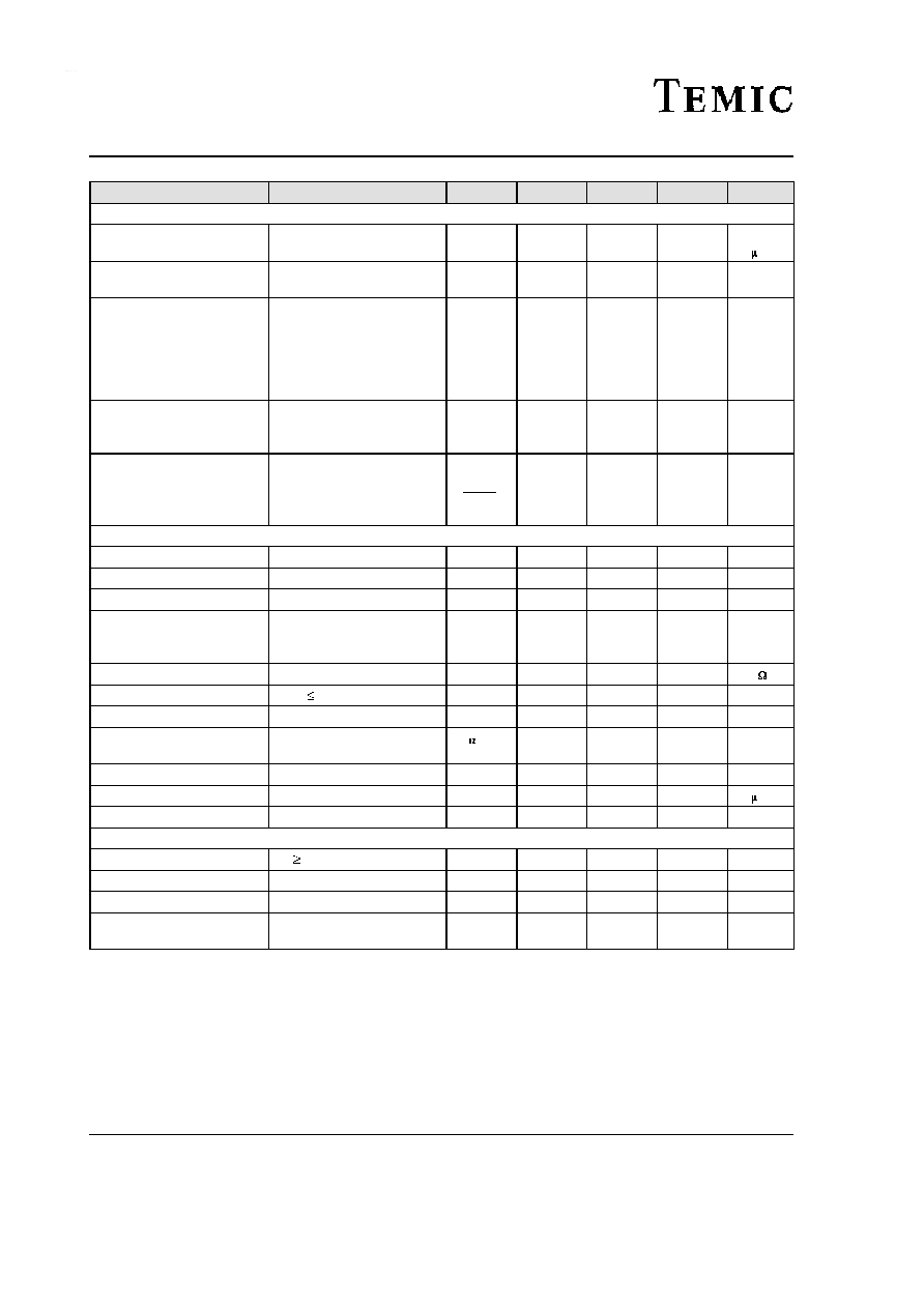
TELEFUNKEN Semiconductors
TDA4481-D
Rev. A1: 23.02.1995
4 (10)
Parameters
Test Conditions / Pins
Symbol
Min.
Typ.
Max.
Unit
FM-operation
Min. sound carrier input
voltage
(intercarrier voltage �3 dB)
Pin 18, 19
v
50
V
Picture carrier input volt-
age
Pin 1�2
v
10
20
30
mV
Audio output voltage
f
PC
= 38.9 MHz, Pin 7, 9
v
1�2
= 20 mV,
f
SC
=33.4 MHz,
v
18�19
= 10 mV,
FM-deviation = 27 kHz,
f
mod
= 1 kHz, Q
B
= 22
v
500
mV
Harmonic distortion
f
mod
= 1 kHz,
Pin 7, 9
Q
B
= 22
FM-deviation = 30 kHz
d
0.5
%
Signal to noise ratio
Standard B/G
according to CCIR 468
specification
FM-deviation 30 kHz,
f
mod
= 1 kHz
Pin 7, 9
Black burst
Grid test signal
(
S+N)
N
62
50
dB
1
)
AF amplifier � SCART-operation
Volume control range
Pin 7
80
dB
V
8
for V
AFmin
at Pin
7
Pin 8
V
8
0
0.5
V
V
8
for V
AFmax
at Pin 7
Pin 8
V
8
4.5
V
SCART control voltage
Pin 3
recording
playback
V
3
V
3
0
4
2
V
SCART input resistance
Pin 5
R
S
55
k
AF input voltage
THD 3 %
Pin 5
v
2
V
SCART-amplification
G
�1
0
+1
dB
Attenuation
v
5
= 500 mV,
Pin 7, 9
V
3
= 0 V
7,9
60
75
dB
Muting on (AF off)
Pin 17
V
17
0
1
V
Switching current
Pin 17
I
17
600
A
Muting off
voltage to diode Pin 17
V
17
4
V
S
V
Converter operation
Pin 10
DC at oscillator pin
V
6
3.5 V
V
10
2.7
V
Oscillator frequency range
f
9
13
MHz
2
)
Oscillator amplitude
v
400
mV
2
)
Operation quality factor of
external oscillator stage
Q
B
70
1)
Standard B/G IF-modulated-FBAS-signal
2)
See application circuit

TELEFUNKEN Semiconductors
TDA4481-D
Rev. A1: 23.02.1995
5 (10)