 | –≠–ª–µ–∫—Ç—Ä–æ–Ω–Ω—ã–π –∫–æ–º–ø–æ–Ω–µ–Ω—Ç: TDA4471 | –°–∫–∞—á–∞—Ç—å:  PDF PDF  ZIP ZIP |

TELEFUNKEN Semiconductors
TDA4471
Preliminary Information
Rev. A1: 18.08.1995
1 (16)
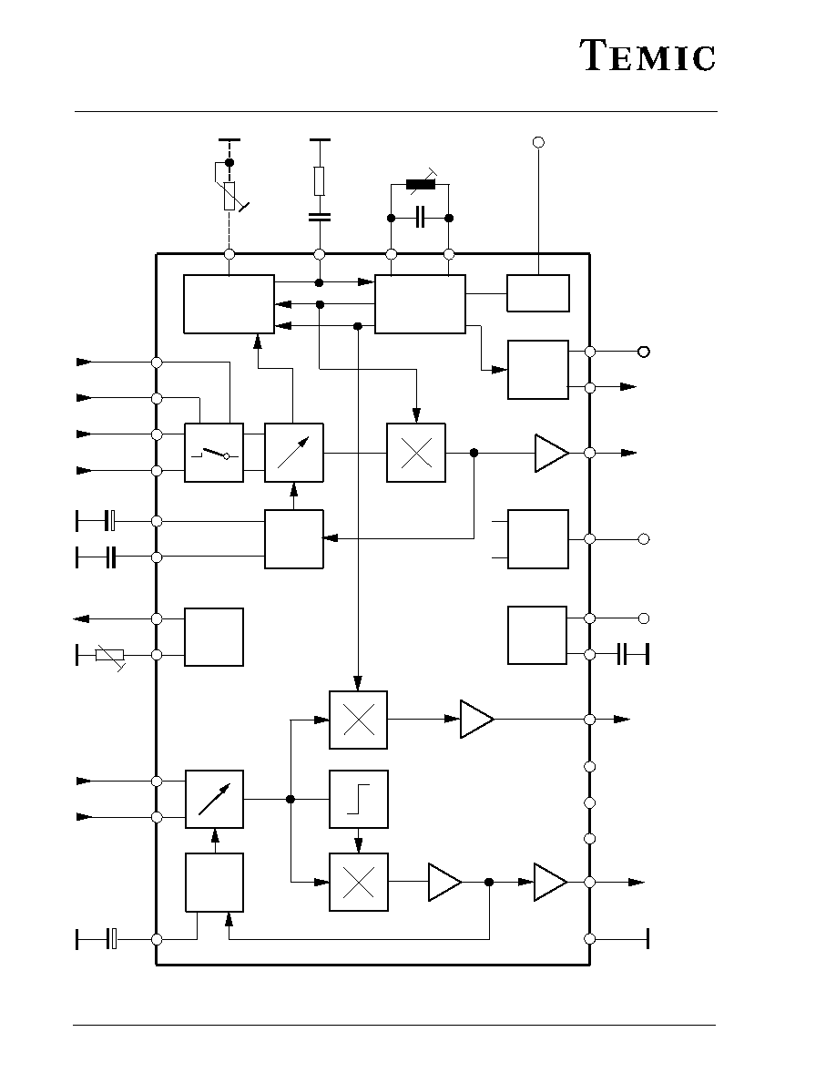
Multistandard Video-IF and Quasi Parallel Sound Processing
Description
The TDA4471 is an integrated bipolar circuit for full
multistandard video/sound IF (VIF/SIF) signal
processing in TV/VCR and Multimedia applications. The
circuit processes all TV video IF signals with negative
modulation (e.g. B/G standard), positive modulation
(e.g. L standard) and the AM, FM/NICAM sound IF
signals. Specially two video IF inputs (2 x VIF) in
combination with one sound IF input (1 x SIF) and the
common pinning with the TDA4474 gives flexibility to
design a universal IF module for various applications.
Features
D
5V supply voltage; low power consumption
D
Active carrier generation by FPLL principle
(frequency≠phase≠locked≠loop) for true
synchronous demodulation
D
Very linear video demodulation, good pulse
response and excellent intermodulation figures
D
VCO circuit is operating on picture carrier
frequency, the VCO frequency is switchable for
the L' mode
D
Alignment≠free AFC without external reference
circuit, polarity of the AFC curve is switchable
D
VIF≠AGC for negative modulated signals
(peak sync detection) and for positive modulation
(peak white/black level detector)
D
Tuner AGC with adjustable take over point
D
Alignment≠free quasi parallel sound (QPS) mixer
for FM/NICAM sound IF signals
D
Intercarrier output signal is gain controlled
(necessary for digital sound processing)
D
Complete alignment≠free AM demodulator with
gain controlled AF output
D
Separate SIF≠AGC with average detection
D
Parallel operation of the AM demodulator and
QPS mixer (for NICAM≠L stereo sound)
D
Two video IF inputs (2 x VIFin)
D
One sound IF input (1 x SIFin)
D
Package and relevant pinning is compatible with
the TDA4474; simplifies the design of an
universal IF module
Package:
30 pin shrink≠dual≠inline≠plastic (SDIP30)
TELEFUNKEN Semiconductors
TDA4471
Preliminary Information
Rev. A1: 18.08.1995
2 (16)
œ
œ
œ
œ
œ
œ
œœ
œœ
AGC
(VIF)
Tuner
AGC
œœ
œ
œœ
œœ
œœ
œœ
AGC
(SIF)
œ
œ
œ
œ
œ
œ
œ
œ
13
12
Tuner
œ
œ
5
SIF 1
VCO
+
phase shift
AFC
Standard
Supply
œœ
œœ
œœ
L' switch
VCO
23
22
20
Loop
filter
16
Offset
comp.
(optional)
28
FPLL
0
∞
90
∞
VIF amp
6
7
8
17
VIF 1
C
AGC
C
BL
Take over
point
C
AGC
24
14
4,9,18
15
Standard
switch
25
V
S
œ
19
C
Re
f
Intercarrier
(FM / NICAM)
26
FM det.
AM det.
SIF amp
27
AF (AM)
AFC
Video
95 9702
œœ
œœ
Video det.
Control
and VIF input switch
œœ
œœ
21
AFC
switch
œ
œ
œ
10
11
VIF 2
œ
œ
œ
œ
œ
œ
2
1
œœ
œœ
œœ
29
30
œœ
œœ
3
n.c.
n.c.
n.c.
œœ
œœ
œœ
œœ
Figure 1.
Block diagram

TELEFUNKEN Semiconductors
TDA4471
Preliminary Information
Rev. A1: 18.08.1995
3 (16)
Pin Description
Pin
Symbol
Function
¡¡¡
¡¡¡
1, 2
¡¡¡¡¡
¡¡¡¡¡
V
i,SIF1
¡¡¡¡¡¡¡¡¡¡
¡¡¡¡¡¡¡¡¡¡
SIF1 input (symmetrical)
¡¡¡
¡¡¡
3
¡¡¡¡¡
¡¡¡¡¡
n.c.
¡¡¡¡¡¡¡¡¡¡
¡¡¡¡¡¡¡¡¡¡
not connected
¡¡¡
4
¡¡¡¡¡
GND
¡¡¡¡¡¡¡¡¡¡
Ground
¡¡¡
¡¡¡
5
¡¡¡¡¡
¡¡¡¡¡
C
AGC
¡¡¡¡¡¡¡¡¡¡
¡¡¡¡¡¡¡¡¡¡
SIF≠AGC (time constant)
¡¡¡
¡¡¡
6, 7
¡¡¡¡¡
¡¡¡¡¡
V
i,VIF1
¡¡¡¡¡¡¡¡¡¡
¡¡¡¡¡¡¡¡¡¡
VIF1 input (symmetrical)
¡¡¡
¡¡¡
8
¡¡¡¡¡
¡¡¡¡¡
C
AGC
¡¡¡¡¡¡¡¡¡¡
¡¡¡¡¡¡¡¡¡¡
VIF≠AGC (time constant)
¡¡¡
¡¡¡
9
¡¡¡¡¡
¡¡¡¡¡
GND
¡¡¡¡¡¡¡¡¡¡
¡¡¡¡¡¡¡¡¡¡
Ground
¡¡¡
¡¡¡
10, 11
¡¡¡¡¡
¡¡¡¡¡
V
i,VIF2
¡¡¡¡¡¡¡¡¡¡
¡¡¡¡¡¡¡¡¡¡
VIF2 input (symmetrical)
¡¡¡
¡¡¡
12
¡¡¡¡¡
¡¡¡¡¡
R
top
¡¡¡¡¡¡¡¡¡¡
¡¡¡¡¡¡¡¡¡¡
Take over point, tuner AGC
¡¡¡
¡¡¡
13
¡¡¡¡¡
¡¡¡¡¡
I
tun
¡¡¡¡¡¡¡¡¡¡
¡¡¡¡¡¡¡¡¡¡
Tuner AGC output current
¡¡¡
¡¡¡
14
¡¡¡¡¡
¡¡¡¡¡
V
o,vid
¡¡¡¡¡¡¡¡¡¡
¡¡¡¡¡¡¡¡¡¡
Video output
¡¡¡
15
¡¡¡¡¡
V
sw
¡¡¡¡¡¡¡¡¡¡
Standard switch
¡¡¡
¡¡¡
16
¡¡¡¡¡
¡¡¡¡¡
V
sw
¡¡¡¡¡¡¡¡¡¡
¡¡¡¡¡¡¡¡¡¡
L'≠/VIF input selector switch
¡¡¡
¡¡¡
17
¡¡¡¡¡
¡¡¡¡¡
C
bl
¡¡¡¡¡¡¡¡¡¡
¡¡¡¡¡¡¡¡¡¡
Capacitor ≠ black level detector
¡¡¡
¡¡¡
18
¡¡¡¡¡
¡¡¡¡¡
GND
¡¡¡¡¡¡¡¡¡¡
¡¡¡¡¡¡¡¡¡¡
Ground
¡¡¡
19
¡¡¡¡¡
C
ref
¡¡¡¡¡¡¡¡¡¡
Internal reference voltage
¡¡¡
¡¡¡
20
¡¡¡¡¡
¡¡¡¡¡
LF
¡¡¡¡¡¡¡¡¡¡
¡¡¡¡¡¡¡¡¡¡
Loop filter
¡¡¡
¡¡¡
21
¡¡¡¡¡
¡¡¡¡¡
V
sw
¡¡¡¡¡¡¡¡¡¡
¡¡¡¡¡¡¡¡¡¡
AFC switch
¡¡¡
¡¡¡
22, 23
¡¡¡¡¡
¡¡¡¡¡
V
vco
¡¡¡¡¡¡¡¡¡¡
¡¡¡¡¡¡¡¡¡¡
VCO circuit
¡¡¡
24
¡¡¡¡¡
V
AFC
¡¡¡¡¡¡¡¡¡¡
AFC output
¡¡¡
¡¡¡
25
¡¡¡¡¡
¡¡¡¡¡
V
s
¡¡¡¡¡¡¡¡¡¡
¡¡¡¡¡¡¡¡¡¡
Supply voltage
¡¡¡
¡¡¡
26
¡¡¡¡¡
¡¡¡¡¡
V
o,FM
¡¡¡¡¡¡¡¡¡¡
¡¡¡¡¡¡¡¡¡¡
Intercarrier output
¡¡¡
¡¡¡
27
¡¡¡¡¡
¡¡¡¡¡
V
o,AM
¡¡¡¡¡¡¡¡¡¡
¡¡¡¡¡¡¡¡¡¡
AF output ≠ AM sound
¡¡¡
¡¡¡
28
¡¡¡¡¡
¡¡¡¡¡
R
comp
¡¡¡¡¡¡¡¡¡¡
¡¡¡¡¡¡¡¡¡¡
Offset compensation
¡¡¡
¡¡¡
29
¡¡¡¡¡
¡¡¡¡¡
n.c.
¡¡¡¡¡¡¡¡¡¡
¡¡¡¡¡¡¡¡¡¡
not connected
¡¡¡
¡¡¡
30
¡¡¡¡¡
¡¡¡¡¡
n.c.
¡¡¡¡¡¡¡¡¡¡
¡¡¡¡¡¡¡¡¡¡
not connected
1
2
3
4
5
6
7
8
10
9
29
24
23
22
20
21
19
12
11
30
27
28
25
26
V
i,VIF1
V
i,VIF1
C
AGC
GND
V
i,VIF2
V
i,VIF2
GND
C
AGC
R
top
n.c.
V
i,SIF1
V
i,SIF1
V
S
V
AFC
V
VCO
V
VCO
V
SW
LF
V
o,AM
V
o,FM
C
Ref
R
comp
n.c.
n.c.
18
17
14
13
95 9703
I
tun
V
o,vid
GND
C
bl
16
15
V
SW
(stand.)
V
SW
(L')
Figure 2. Pin configuration

TELEFUNKEN Semiconductors
TDA4471
Preliminary Information
Rev. A1: 18.08.1995
4 (16)
Circuit Description
Vision IF amplifier
The video IF signal (VIF) is fed through a SAW filter to
one of the two VIF inputs (Pins 6≠7 or 10≠11). The
selection of VIF input is controlled by Pin 16 in combina-
tion with the standard switch. With a minimal external
expense it is possible to switch between two different
SAW filters. Both VIF inputs features excellent
cross≠talk attenuation and an input impedance which is
independent from the switching condition. The VIF
amplifier consists of three AC≠coupled amplifier stages.
Each differential amplifier is gain controlled by the
automatic gain control (VIF≠AGC). Output signal of the
VIF amplifier is applied to the FPLL carrier generation
and the video demodulator.
Tuner≠ and VIF≠AGC
At Pin 8 the VIF≠AGC charges/discharges the AGC
capacitor to generate a control voltage for setting gain of
VIF amplifier and tuner in order to keep the video output
signal at a constant level. Therefore in case of negative
modulated signals (e.g. B/G standard) the sync level of
the demodulated video signal is the criterion for a fast
charge/discharge of the AGC capacitor. For positive mod-
ulation (e.g. L standard) the peak white level of video
signal controls the charge current. In order to reduce
reaction time for positive modulation, where a very large
time constant is needed, an additional black level detector
(Pin 17) controls the discharge current in the event of
decreasing VIF input signal. The AGC voltage is
transferred to an internal control signal, and is fed to the
tuner AGC to generate the tuner AGC current at Pin 13
(open collector output).
Take over point of the tuner AGC can be adjusted at
Pin 12 by a potentiometer or an
external DC voltage
(from interface circuit or microprocessor).
FPLL, VCO and AFC
The FPLL circuit (frequency phase locked loop) consists
of a frequency and phase detector to generate control
voltage for the VCO tuning. In the locked mode the VCO
is controlled by the phase detector and in unlocked mode
the frequency detector is superimposed. The VCO
operates with an external resonance circuit (L and C
parallel) and is controlled by internal varicaps. The VCO
control voltage is also converted to a current and
represents the AFC output signal at Pin 24. With the AFC
switch (Pin 21) three operating conditions of the AFC are
possible: AFC curve "rising" or "falling" and AFC "off".
A practicable VCO alignment of the external coil is the
adjustment to zero AFC output current at Pin 24. At centre
frequency the AFC output current is equal to zero. Fur-
thermore, at Pin 16, the VCO centre frequency can be
switched for setting to the required L' value This function
is active when "L mode" is selected by the standard
switch.
The optional potentiometer at Pin 28 allows an offset
compensation of the VCO phase for improved sound
quality (fine adjustment). Without a potentiometer (open
circuit at Pin 28) this offset compensation is not active.
The oscillator signal passes a phase shifter and supplies
the in≠phase signal (0) and the quadrature signal (90) of
the generated picture carrier.
Video demodulation and amplifier
The video IF signal, which is applied from the gain
controlled IF amplifier, is multiplied with the inphase
component of the VCO signal. The video demodulator is
designed for low distortion and large bandwidth. The
demodulator output signal passes an integrated low pass
filter for attenuation of the residual vision carrier and is
fed to the video amplifier. The video amplifier is realized
by an operational amplifier with internal feedback and
8 MHz bandwidth (≠3dB). A standard dependent DC
level shift in this stage delivers the same sync level for
positive and negative modulation. An additional noise
clipping is provided. The video signal is fed to VIF≠AGC
and to the video output buffer. This amplifier with 6dB
gain offers easy adaption of the sound trap. For nominal
video IF modulation the video output signal at Pin 14 is
2 V (peak to peak value).
Sound IF amplifier and SIF≠AGC
The SIF amplifier is nearly identical with the 3≠stage VIF
amplifier. Each differential amplifier is gain controlled
by the automatic gain control for the sound IF path (SIF≠
AGC). Output signal of the SIF amplifier is applied to the
mixer for FM/NICAM signals and the limiter/
demodulator for AM signals.
The SIF≠AGC is related to the average level of AM≠ or
FM≠carrier and controls the SIF amplifier to provide a
constant SIF signal to the AM demodulator and QPS
mixer.
AM demodulator
The alignment≠free AM demodulator is realized by a syn-
chronous detector. The modulated SIF signal from the SIF
amplifier output is multiplied in phase with the limited
SIF signal (AM is removed). The AF signal of the
demodulator output is fed to the output amplifier and to
the SIF≠AGC. For all TV standards with negative video
TELEFUNKEN Semiconductors
TDA4471
Preliminary Information
Rev. A1: 18.08.1995
5 (16)
modulation (e.g. B/G standard) the AF output signal
(Pin 27) is switched off by the standard switch.
Quasi≠Parallel≠Sound (QPS) mixer
The QPS mixer is realized by a multiplier. The SIF signal
(FM or NICAM carrier) is converted to the intercarrier
frequency by the regenerated picture carrier (quadrature
signal) which is provided from the VCO. The intercarrier
signal is fed via an output amplifier to Pin 26.
Standard switch
To have equal polarity of the video output signal the po-
larity can be switched in the demodulation stage in
accordance with the TV standard. Additional a standard
dependent DC level shift in the video amplifier delievers
the same sync level. Parallel the correct VIF≠AGC is se-
lected for positive or negative modulated VIF signals. In
case of negative modulation (e.g. B/G standard) the AM
output signal is switched off. If the standard for positive
modulation (L standard) is selected the AM demodulator
and QPS mixer is active. This condition allows a parallel
operation of the AM sound signal and the NICAM≠L ste-
reo sound.
L' switch and VIF input selection
For positive modulated IF signals (L/L' standard) Pin 16
works as L' switch. With a control voltage at Pin 16 the
VCO frequency can be switched for setting to the required
L' value (L' standard). Also a fine adjustment of the L'≠
VCO centre frequency is possible by a potentiometer. The
L' switch is only active for positive modulated video IF
signals (standard switch in L mode). In this mode the
video IF input 2 (VIF2) is forced by the standard switch.
The possibility to select VIF1 input is given by connect-
ing VIF2 input (pin 10 or 11) via 10 k resistor to ground.
If negative modulation (B/G mode) is selected pin 16 op-
erates as an input selection switch for the two VIF inputs.
AFC switch
The AFC output signal at Pin 24 can be controlled by a
switching voltage at Pin 21. It is possible to select an AFC
output signal with rising≠ or falling AFC curve and to
switch off the AFC.
Internal voltage stabilizer
The internal bandgap reference ensures constant perfor-
mance independant of supply voltage and temperature.
Absolute maximum values
Reference point pin 4 (9, 18), unless otherwise specified
Parameters
Symbol
Value
Unit
¡¡¡¡¡¡¡¡¡¡¡¡¡¡¡¡¡
¡
¡¡¡¡¡¡¡¡¡¡¡¡¡¡¡
¡
Supply voltage
Pin 25
¡¡¡¡¡
¡
¡¡¡
¡
V
S
¡¡¡¡¡¡¡¡
¡
¡¡¡¡¡¡
¡
9.0
¡¡¡¡¡
¡
¡¡¡
¡
V
¡¡¡¡¡¡¡¡¡¡¡¡¡¡¡¡¡
¡¡¡¡¡¡¡¡¡¡¡¡¡¡¡¡¡
Supply current
Pin 25
¡¡¡¡¡
¡¡¡¡¡
I
S
¡¡¡¡¡¡¡¡
¡¡¡¡¡¡¡¡
85
¡¡¡¡¡
¡¡¡¡¡
mA
¡¡¡¡¡¡¡¡¡¡¡¡¡¡¡¡¡
¡¡¡¡¡¡¡¡¡¡¡¡¡¡¡¡¡
Power dissipation, V
s
= + 9 V
¡¡¡¡¡
¡¡¡¡¡
P
¡¡¡¡¡¡¡¡
¡¡¡¡¡¡¡¡
765
¡¡¡¡¡
¡¡¡¡¡
mW
¡¡¡¡¡¡¡¡¡¡¡¡¡¡¡¡¡
¡¡¡¡¡¡¡¡¡¡¡¡¡¡¡¡¡
Output currents
Pin 14, 26, 27
¡¡¡¡¡
¡¡¡¡¡
I
out
¡¡¡¡¡¡¡¡
¡¡¡¡¡¡¡¡
5
¡¡¡¡¡
¡¡¡¡¡
mA
¡¡¡¡¡¡¡¡¡¡¡¡¡¡¡¡¡
¡
¡¡¡¡¡¡¡¡¡¡¡¡¡¡¡
¡
¡¡¡¡¡¡¡¡¡¡¡¡¡¡¡¡¡
External voltages
Pins 1, 2, 5≠8, 10≠12,
14, 16, 19, 20, 26≠28
¡¡¡¡¡
¡
¡¡¡
¡
¡¡¡¡¡
V
ext
¡¡¡¡¡¡¡¡
¡
¡¡¡¡¡¡
¡
¡¡¡¡¡¡¡¡
+ 4.5
¡¡¡¡¡
¡
¡¡¡
¡
¡¡¡¡¡
V
¡¡¡¡¡¡¡¡¡¡¡¡¡¡¡¡¡
¡¡¡¡¡¡¡¡¡¡¡¡¡¡¡¡¡
Pins 17, 22, 23
¡¡¡¡¡
¡¡¡¡¡
¡¡¡¡¡¡¡¡
¡¡¡¡¡¡¡¡
+ 3.5
¡¡¡¡¡
¡¡¡¡¡
V
¡¡¡¡¡¡¡¡¡¡¡¡¡¡¡¡¡
Pins 13
¡¡¡¡¡
¡¡¡¡¡¡¡¡
+ 13.5
¡¡¡¡¡
V
¡¡¡¡¡¡¡¡¡¡¡¡¡¡¡¡¡
¡¡¡¡¡¡¡¡¡¡¡¡¡¡¡¡¡
Pins 15, 21, 24
¡¡¡¡¡
¡¡¡¡¡
¡¡¡¡¡¡¡¡
¡¡¡¡¡¡¡¡
V
s
¡¡¡¡¡
¡¡¡¡¡
V
¡¡¡¡¡¡¡¡¡¡¡¡¡¡¡¡¡
¡¡¡¡¡¡¡¡¡¡¡¡¡¡¡¡¡
Junction temperature
¡¡¡¡¡
¡¡¡¡¡
T
j
¡¡¡¡¡¡¡¡
¡¡¡¡¡¡¡¡
+125
¡¡¡¡¡
¡¡¡¡¡
∞
C
¡¡¡¡¡¡¡¡¡¡¡¡¡¡¡¡¡
¡¡¡¡¡¡¡¡¡¡¡¡¡¡¡¡¡
Storage temperature
¡¡¡¡¡
¡¡¡¡¡
T
stg
¡¡¡¡¡¡¡¡
¡¡¡¡¡¡¡¡
≠25 to +125
¡¡¡¡¡
¡¡¡¡¡
∞
C
¡¡¡¡¡¡¡¡¡¡¡¡¡¡¡¡¡
¡¡¡¡¡¡¡¡¡¡¡¡¡¡¡¡¡
Electrostatic handling *)
All pins
¡¡¡¡¡
¡¡¡¡¡
V
ESD
¡¡¡¡¡¡¡¡
¡¡¡¡¡¡¡¡
300
¡¡¡¡¡
¡¡¡¡¡
V
*) Equivalent to discharging a 200 pF capacitor through a 0 resistor
Operating Range
Parameters
Symbol
Value
Unit
¡¡¡¡¡¡¡¡¡¡¡¡¡¡¡¡¡
¡¡¡¡¡¡¡¡¡¡¡¡¡¡¡¡¡
Supply voltage range25
¡¡¡¡¡
¡¡¡¡¡
V
S
¡¡¡¡¡¡¡¡
¡¡¡¡¡¡¡¡
4.5 to 9.0
¡¡¡¡¡
¡¡¡¡¡
V
¡¡¡¡¡¡¡¡¡¡¡¡¡¡¡¡¡
¡¡¡¡¡¡¡¡¡¡¡¡¡¡¡¡¡
Ambient temperature
¡¡¡¡¡
¡¡¡¡¡
T
amb
¡¡¡¡¡¡¡¡
¡¡¡¡¡¡¡¡
0 to +85
¡¡¡¡¡
¡¡¡¡¡
∞
C