TELEFUNKEN Semiconductors
TDA 4480-C
1
Preliminary Information
Multi standard quasi parallel-sound processor for TV-sets
Technology:
Bipolar
Features
D High signal sensitivity
D Simple filter configuration and few external
components
D Processing of two carrier stereo signals
D Low intercarrier distortions
D ESD protected
D Alignment free AM demodulator for the standard L
D VCO controlled mixer stage converts intercarrier
frequencies of different standards into a preferred
sound IF
D Optimum tuning characteristic
Case: 20-pin dual inline plastic
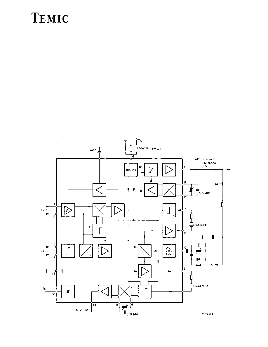
Figure 1 Block diagram

TELEFUNKEN Semiconductors
TDA 4480-C
2
Preliminary Information
Pin Configuration
Pin
Symbol
Function
1�2
Vision-IF-carrier input
3
Intercarrier input 5.74 MHz
4
AGC time constant
5
Intercarrier output 5.74 MHz
6
Standard switch
7
AF output 1
8-9
Phase tank circuit 5.74 MHz
10
VC0 tank circuit
Pin
Symbol
Function
11
Ground
12-13
Phase tank circuit 5.5 MHz
14
AF output 2
15
Intercarrier output 5.5 MHz
16
Supply voltage
17
Intercarrier input 5.5 MHz
18-19
Sound-IF-carrier input
20
n.c.
Circuit Description
The integrated circuit allows the high quality processing of sound carrier for different TV standards. The circuit requires
separate vision and audio carrier inputs. It delivers the output audio signal for mono, two channels or stereo applications.
Audio carrier signal (simple or double carrier, FM and AM) is applied via three stage AGC controlled broad band amplifier
which delivers regulated output signal for two mixing stages. One mixer works for AM-demodulation and AGC-function
whereas the second mixer produces the sound intercarrier IF-frequencies (5.5/5.74 MHz).
Vision carrier signal for the intercarrier generation is delivered from the demodulator tank of the video IF circuit (TDA
4439, TDA 4453). It is then matched via a limiter stage to the FM intercarrier mixer. FM-sound-IF-carrier reaches the
quadrature demodulator via the selection circuit and the following limiter amplifier. The final audio signal is supplied
to the low ohmic output (Pin 7,14) with low pass filter character.
There is a switchable converter for different audio standards (4.5, 6.00 and 6.5 MHZ), which mixes the sound 1P-signal
properly e.g. at 5.5 MHz. The VC0 (Pin 10) must be controlled across the sound output (Pin 7) which includes
AFC-function.
Sound signal at the AM-modulation is introduced via standard switch in the first sound channel, whereas the intercarrier,
converter section and both FM demodulators are switched off. In case of sound IF converter operation, the second sound
channel and the AM-section are switched off. The standard mode is controlled by a tristate signal on Pin 6.
Absolute Maximum Ratings
Reference point Pin 11, unless otherwise specified
Parameters
Symbol
Value
Unit
Supply voltage
Pin 16
V
S
10 to 13.5
V
Supply current
Pin 16
I
S
80
mA
External voltage
Pin 6
Pin 1, 2, 3, 4, 5, 7, 8, 9, 12,
13, 14, 15, 17, 18, 19
V
ext
V
ext
V
S
6
V
V
Power dissipation
(in soldered position)
P
tot
1
W
Junction temperature
T
j
125
_
C
Ambient temperature range
T
amb
- 25 to + 70
_
C
Storage temperature range
T
stg
- 25 to + 125
_
C
TELEFUNKEN Semiconductors
TDA 4480-C
3
Preliminary Information
Thermal Resistance
Parameters
Symbol
Value
Unit
Junction ambient
R
thJA
60
K/W
Electrical Characteristics
V
5
= 12 V, T
amb
= 25
_
C, reference point pin 11, f
PC
= 38.9 MHz, f
SC1
= 33.4 MHz, f
SC2
= 33.1578 MHz,
SC1/SC2 = 7 dB, unless otherwise specified
Parameters
Test Conditions / Pin
Symbol
Min
Type
Max
Unit
Supply voltage range
Pin 16
V
S
10
13.5
V
Supply current
FM-operation,
Pin 16
AM-operation,
Pin 16
I
S
I
S
65
40
mA
mA
Output DC voltage
Pin 7,14
V
0
3.5
V
Standard switching voltage
Standard B/G,
Pin 6
Standard L,
Pin 6
converter operation Pin 6
V
V
V
1.7
0
3.5
2.2
2.7
1.5
V
S
V
V
V
Standard switching current
V
6
x 5 V
Pin 6
I
20
mA
Picture carrier input voltage
Pin 1,2
v
5
10
20
mV
Min. sound carrier input
voltage SC1
5.5 MHz-output
Pin 18,19
signal �3 dB
v
50
mV
Max. sound carrier input
voltage SC1
Pin 18,19
v
100
mV
AGC range
65
dB
Audio output voltage
FM-deviation = 30 kHz
m = 80 %
Pin 7,14
v
500
mV
eff
Audio voltage difference
between both outputs
Pin 7,14
v
"1
dB
Harmonic distortion AM-
operation
f
mod
= 1 kHz,
Pin 7,14
FM-deviation = 30 kHz
d
0.5
%
Harmonic distortion AM-
operation
f
mod
= 1 kHz,
Pin 7
m = 80 %, v
18-19
= 10 mV
d
1.5
3.0
%
Min. output load
Pin 7,14
R
3
k
W
Signal to noise ratio (Standard B/G) according to
CCIR 468-2 specifications, SC1: v
18-19
= 10 mV,
PC: v
1-2
= 10 mV, prelimited demodulator picture carrier
signal from TDA 4453 reference signal: f
mod
= 1 kHz,
FM deviation = 30 kHz
Black burst
1. channel/2. channel
1)
Pin 7/14
(S=N)/N
62/60
dB
Grid test signal
1. channel/2. channel
1)
Pin 7/14
(S=N)/N
50/48
dB
Converter
DC voltage
V
6
y 3.5 V
Pin 10
V
10
2.7
V
Tuning range
Pin 10
f
9
13
MHz
Input resistance
Pin 10
R
100
k
W
Input capacity
Pin 10
C
12
pF
TELEFUNKEN Semiconductors
TDA 4480-C
4
Preliminary Information
Parameters
Test Conditions / Pin
Symbol
Min
Type
Max
Unit
Signal to noise ratio (Standard B/G) according to
CCIR 468-2 specifications, SC1: v
18-19
= 10 mV,
PC: v
1-2
= 10 mV, prelimited demodulator picture carrier
signal from TDA 4453 reference signal: f
mod
= 1 kHz,
FM deviation = 30 kHz
Black burst
1. channel/2. channel
1)
Pin 7/14
(S=N)/N
62/60
dB
Grid test signal
1. channel/2. channel
1)
Pin 7/14
(S=N)/N
50/48
dB
Converter
DC voltage
V
6
y 3.5 V
Pin 10
V
10
2.7
V
Tuning range
Pin 10
f
9
13
MHz
Input resistance
Pin 10
R
100
k
W
Input capacity
Pin 10
C
12
pF
1)
Standard B/G IF-modulated FBAS-signal
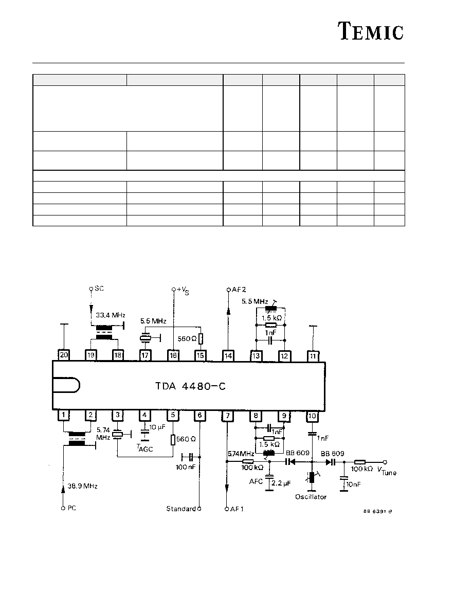
Figure 2: Test circuit
TELEFUNKEN Semiconductors
TDA 4480-C
5
Preliminary Information
Pin 1,2
IF-input
vision carrier
Pin 18,19
IF-input
sound carrier
Pin 3 (17)
Intercarrier input
Pin 3: 5.74 MHz
Pin 17: 5.5 MHz