TSC8051C1
Rev. D (14 Jan. 97)
1
MATRA MHS
1. Introduction
The TSC8051C1 is a stand≠alone high performance
CMOS 8≠bit embedded microcontroller and is designed
for use in CRT monitors. It is also suitable for automotive
and industrial applications.
The TSC8051C1 includes the fully static 8≠bit "80C51"
CPU core with 256 bytes of RAM; 8 Kbytes of ROM; two
16≠bit timers; 12 PWM Channels; a 6 sources and 2≠level
interrupt controller; a full duplex serial port; a full I
2
C
TM
*
interface; a watchdog timer and on≠chip oscillator.
In addition, the TSC8051C1 has 2 software selectable
modes of reduced activity for further reduction in power
consumption. In the idle mode the CPU is frozen while
the RAM, the timers, the serial ports, and the interrupt
system continue to function. In the power down mode the
RAM is saved and all other functions are inoperative.
The TSC8051C1 enables the users reducing a lot of
external discrete components while bringing the
maximum of flexibility.
2. Features
D Boolean processor
D Fully static design
D 8K bytes of ROM
D 256 bytes of RAM
D 2 x 16≠bit timer/counter
D Programmable serial port
D Programmable Multimaster I
2
C controller
D 6 interrupt sources:
G External interrupts (2)
G Timers interrupt (2)
G Serial port interrupt
G I
2
C interrupt
D Watchdog reset
D On chip oscillator for crystal or ceramic resonator
D 2 power saving control modes:
G Idle mode
G Power≠down mode
D Controlled HSYNC & VSYNC outputs
D Up to 12 programmable PWM channels with 8≠bit
resolution
D Up to 32 programmable I/O lines depending on the
package
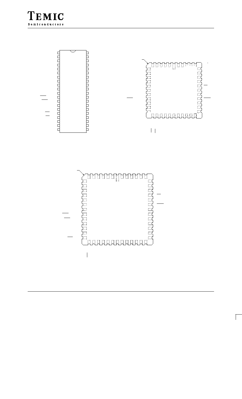
D 40 pins DIP, 44 pins PQFP, 44 and 52 pins PLCC
packages
D Commercial and industrial temperature ranges
D Operating Frequency: 12 MHz to 16 MHz
8-Bit Microcontroller for Digital Computer Monitors
* I2C is a trademark of PHILIPS Corporation
TSC8051C1
Rev. D (14 Jan. 97)
4
MATRA MHS
5. Pin Description
VSS
Circuit ground.
VCC
Power supply voltage.
RST
A high level on this pin for two machine cycles while the
oscillator is running resets the device. An internal
pulldown resistor permits power≠on reset using only a
capacitor connected to VCC.
PORT 0 (P0.0≠P0.7)
Port 0 is an 8≠bit open≠drain bidirectional I/O port. Port
0 pins that have 1's written to them float, and in that state
can be used as high≠impedance inputs.
Port 0 is also the multiplexed low≠order address and data
bus during access to external Program and Data memory.
In this application it uses strong internal pull≠up when
emitting 1's.
Port 0 can sink and source 8 LS TTL loads.
PORT 1 (P1.0≠P1.7)
Port 1 is an 8≠bit bidirectional I/O port with internal
pullups. Port 1 pins that have 1's written to them are
pulled high by the internal pullups, and in that state can
be used as inputs. As inputs, Port 1 pins that are
externally being pulled low will source current (IIL on
the data≠sheet) because of the internal pullups.
Port 1 also serves 4 programmable PWM open drain
outputs, as listed below:
Port Pin
Alternate Function
P1.0
PWM8: Pulse Width Modulation output 8.
P1.1
PWM9: Pulse Width Modulation output 9.
P1.2
PWM10: Pulse Width Modulation output 10.
P1.3
PWM11: Pulse Width Modulation output 11.
Port 1 can sink and source 3 LS TTL loads.
PORT 2 (P2.0≠P2.7)
Port 2 is an 8≠bit bidirectional I/O port with internal
pullups. Port 2 pins that have 1's written to them are
pulled high by the internal pullups, and in that state can
be used as inputs. As inputs, Port 2 pins that are
externally being pulled low will source current (IIL on
the data≠sheet) because of the internal pullups.
Port 2 emits the high≠order 8≠bit address during fetches
from external Program Memory and during accesses to
external Data Memory that use 16≠bit addresses. In this
application it uses strong internal pull≠up when emitting
1's.
Port 2 can sink and source 3 LS TTL loads.
PORT 3 (P3.0≠P3.7)
Port 3 is an 8≠bit bidirectional I/O port with internal
pullups. Port 3 pins that have 1's written to them are
pulled high by the internal pullups, and in that state can
be used as inputs. As inputs, Port 3 pins that are
externally being pulled low will source current (IIL on
the data≠sheet) because of the internal pullups.
Each line on this port has 2 or 3 functions either a general
I/O or special control signal, as listed below:
Port Pin
Alternate Function
P3.0
RXD: serial input port.
P3.1
TXD: serial output port.
P3.2
INT0: external interrupt 0.
VSYNC: vertical synchro input.
P3.3
INT1: external interrupt 1.
VOUT: buffered V-SYNC output.
P3.4
T0: Timer 0 external input.
HSYNC: horizontal synchro input.
P3.5
T1: Timer 1 external input.
HOUT: buffered H≠SYNC output.
P3.6
WR: external data memory write strobe.
SCL: serial port clock line I
2
C bus.
P3.7
RD: external data memory read strobe.
SDA: serial port data line I
2
C bus.
Port 3 can sink and source 3 LS TTL loads.
PWM0≠7
These eight Pulse Width Modulation outputs are true
open drain outputs and are floating after reset.
ALE
The Address Latch Enable output signal occurs twice
each machine cycle except during external data memory
access. The negative edge of ALE strobes the address
into external data memory or program memory. ALE
can sink and source 8 LS TTL loads.
If desired, ALE operation can be disabled by setting bit
0 of SFR location AFh (MSCON). With the bit set, ALE
is active only during MOVX instruction and external
fetches. Otherwise the pin is pulled low.

TSC8051C1
Rev. D (14 Jan. 97)
5
MATRA MHS
EA
When the External Access input is held high, the CPU
executes out of internal program memory (unless the
Program Counter exceeds 1FFFh). When EA is held low
the CPU executes only out of external program memory.
must not be left floating.
PSEN
The Program Store Enable output signal remains high
during internal program memory. An active low output
occurs during an external program memory fetch. PSEN
can sink and source 8 LS TTL loads.
XTAL1
Input to the inverting oscillator amplifier and input to the
external clock generator circuits.
XTAL2
Output from the inverting oscillator amplifier. This pin
should be non≠connected when external clock is used.