
TSC8051C2
Rev. A (10 Jan. 97)
1
Preview
MATRA MHS
1. Introduction
The TSC8051C2 is a stand≠alone high performance
CMOS 8≠bit embedded microcontroller and is designed
for use in CRT monitors. It is also suitable for automotive
and industrial applications.
The TSC8051C2 includes the fully static 8≠bit "80C51"
CPU core with 256 bytes of RAM; 4 Kbytes of ROM; two
16≠bit timers; 12 PWM Channels; a 5 sources and 2≠level
interrupt controller; a full duplex serial port; a watchdog
timer; power voltage monitor and on≠chip oscillator.
In addition, the TSC8051C2 has 2 software selectable
modes of reduced activity for further reduction in power
consumption. In the idle mode the CPU is frozen while
the RAM, the timers, the serial ports, and the interrupt
system continue to function. In the power down mode the
RAM is saved and all other functions are inoperative.
The TSC8051C2 enables the users reducing a lot of
external discrete components while bringing the
maximum of flexibility.
2. Features
D Boolean processor
D Fully static design
D 4K bytes of ROM
D 256 bytes of RAM
D 2 x 16≠bit timer/counter
D Programmable serial port
D 5 interrupt sources:
D External interrupts (2)
D Timers interrupt (2)
D Serial port interrupt
D Watchdog reset
D Power Fail reset
D On chip oscillator for crystal or ceramic resonator
D 2 power saving control modes:
D Idle mode
D Power≠down mode
D SYNC Processor
D Controlled HSYNC & VSYNC outputs
D Controlled HSYNC & VSYNC inputs
D Clamp pulse output
D Up to 12 programmable PWM channels with 8≠bit
resolution
D Up to 32 programmable I/O lines depending on the
package
D 40 pins DIP, 44 pins PQFP, 44 and 52 pins PLCC
packages
D Commercial and industrial temperature ranges
D Operating Frequency: 12 MHz to 16 MHz
8-Bit Microcontroller for Digital Computer Monitors

TSC8051C2
Rev. A (10 Jan. 97)
2
Preview
MATRA MHS
3. Block Diagram
T1
INT1
T0
ALTERNATE FUNCTION OF PORT0
ALTERNATE FUNCTION OF PORT2
ALTERNATE FUNCTION OF PORT1
ALTERNATE FUNCTION OF PORT3
1
80C51 CORE
EXCLUDING
ROM/RAM
PROGRAM
MEMORY
4k x 8 ROM
DATA
MEMORY
256 x 8 RAM
CLAMP
PULSE
TWO 16≠BIT
TIMER/EVENT
COUNTER
CPU
SERIAL
UART
PORT
PARALLEL I/O
PORTS AND
EXTERNAL BUS
AD0≠7
RST
A8≠15
3
3
0
2
3
3
3
1
3
3
3
3
2
1
0
PWM8
≠
PWM11
PWM0
≠
PWM7
VCC VSS
INT0
T0
CPO
P0 P1 P2 P3 TxD RxD
12 x 8≠bit PWM
CHANNELS
WATCHDOG
TIMER
CONTROLLED
HSYNC & VSYNC
OUTPUTS
XTAL1
XTAL2
EA
ALE
PSEN
WR
RD
SPECIAL
EXTERNAL
INPUTS
3
3
3
3
VSYNC HSYNC
VOUT HOUT
POWER
VOLTAGE
MONITOR
8≠BIT INTERNAL BUS
INT0
Figure 1. TSC8051C2 block diagram.

TSC8051C2
Rev. A (10 Jan. 97)
3
Preview
MATRA MHS
4. Pin Configurations
P3.1/TXD
11
PSEN
12
EA
10
P3.2/INT0/VSYNC
P3.0/RXD
DIL 40
VCC
P0.0/AD0
P0.1/AD1
P0.2/AD2
P0.3/AD3
P0.4/AD4
P0.5/AD5
P0.6/AD6
P0.7/AD7
ALE
PWM7 *
PWM6 *
PWM5 *
PWM4 *
PWM3 *
PWM2 *
PWM1 *
PWM0 *
P1.0/PWM8
P1.1/PWM9
P1.2/PWM10
P1.3/PWM11
P1.4/CPO
P1.5
P1.6
P1.7
RST
P3.3/INT1/VOUT
P3.4/TO/HSYNC
P3.5/T1/HOUT
P3.6/WR
P3.7/RD
XTAL2
XTAL1
VSS
1
2
3
4
5
6
7
8
9
13
14
15
16
17
18
19
20
40
39
38
37
36
35
34
33
23
22
21
29
31
32
28
27
26
25
24
30
*PWMx or P2.x depending on option (see ordering information)
33
32
31
30
29
28
27
26
25
24
23
22
21
20
19
18
17
16
15
14
13
12
11
10
9
8
47
48
49
50
51
52
1
2
3
4
5
6
7
34
35
36
37
38
39
40
41
42
43
44
45
46
PLCC 52
INDEX
CORNER
P0.5
P0.6
P0.7
EA
ALE
PSEN
P2.7
PWM7
P2.6
PWM6
P2.5
PWM5
PWM4
NC
P1.5
P1.6
P1.7
RST
P3.0/RXD
P3.1/TXD
P3.2/INT0/VSYNC
P3.3/INT1/VOUT
P3.4/T0/HSYNC
P3.5/T1/HOUT
NC
P3.6/WR
P1.4/CPO
P1.3/PWM1
1
P1.2/PWM10
P1.1/PWM9
P1.0/PWM8
NC
VCC
P0.0
P0.1
P0.2
P0.3
NC
P0.4
P3.7/RD
XT
AL2
XT
AL1
VSS
PWM0
PWM1
PWM2
PWM3
P2.0
P2.1
P2.2
P2.3
P2.4
Figure 2. TSC8051C2 pin configurations.
2
3
4
5
12
6
7
39
8
9
10
11
35
36
37
38
PLCC 44
P1.5
P1.6
P1.7
RST
P3.0/RXD
NC
P3.1/TXD
P3.2/INT0/VSYNC
PWM7*
PWM6*
PWM5*
28
26 26
24
23
22
21
20
19
18
17
16
15
14
13
40
41
42
43
44
1
29
30
31
32
33
34
INDEX
CORNER
P0.4
P0.5
P0.6
P0.7
EA
NC
ALE
PSEN
PWM7*
PWM6*
PWM5*
27
P1.4/CPO
P1.3/PWM1
1
P1.2/PWM10
P1.1/PWM9
P1.0/PWM8
NC
VCC
P0.0
P0.1
P0.2
P0.3
P3.6/WR
P3.7/RD
XT
AL2
XT
AL1
VSS
NC
PWM0*
PWM1*
PWM2*
PWM3*
PWM4*

TSC8051C2
Rev. A (10 Jan. 97)
4
Preview
MATRA MHS
5. Pin Description
VSS
Circuit ground.
VCC
Power supply voltage.
RST
A high level on this pin for two machine cycles while the
oscillator is running resets the device. An internal
pulldown resistor permits power≠on reset using only a
capacitor connected to VCC.
PORT 0 (P0.0≠P0.7)
Port 0 is an 8≠bit open≠drain bidirectional I/O port. Port
0 pins that have 1's written to them float, and in that state
can be used as high≠impedance inputs.
Port 0 is also the multiplexed low≠order address and data
bus during access to external Program and Data memory.
In this application it uses strong internal pull≠up when
emitting 1's.
Port 0 can sink and source 8 LS TTL loads.
PORT 1 (P1.0≠P1.7)
Port 1 is an 8≠bit bidirectional I/O port with internal
pullups. Port 1 pins that have 1's written to them are
pulled high by the internal pullups, and in that state can
be used as inputs. As inputs, Port 1 pins that are
externally being pulled low will source current (IIL on
the data≠sheet) because of the internal pullups.
Port 1 also serves 4 programmable PWM open drain
outputs and programmable open drain CPO, as listed
below:
Port Pin
Alternate Function
P1.0
PWM8: Pulse Width Modulation output 8.
P1.1
PWM9: Pulse Width Modulation output 9.
P1.2
PWM10: Pulse Width Modulation output 10.
P1.3
PWM11: Pulse Width Modulation output 11.
P1.4
CPO: Clamp Pulse Output.
Port 1 can sink and source 3 LS TTL loads.
PORT 2 (P2.0≠P2.7)
Port 2 is an 8≠bit bidirectional I/O port with internal
pullups. Port 2 pins that have 1's written to them are
pulled high by the internal pullups, and in that state can
be used as inputs. As inputs, Port 2 pins that are
externally being pulled low will source current (IIL on
the data≠sheet) because of the internal pullups.
Port 2 emits the high≠order 8≠bit address during fetches
from external Program Memory and during accesses to
external Data Memory that use 16≠bit addresses. In this
application it uses strong internal pull≠up when emitting
1's.
Port 2 can sink and source 3 LS TTL loads.
PORT 3 (P3.0≠P3.7)
Port 3 is an 8≠bit bidirectional I/O port with internal
pullups. Port 3 pins that have 1's written to them are
pulled high by the internal pullups, and in that state can
be used as inputs. As inputs, Port 3 pins that are
externally being pulled low will source current (IIL on
the data≠sheet) because of the internal pullups.
Each line on this port has 2 or 3 functions either a general
I/O or special control signal, as listed below:
Port Pin
Alternate Function
P3.0
RXD: serial input port.
P3.1
TXD: serial output port.
P3.2
INT0: external interrupt 0.
VSYNC: vertical synchro input.
P3.3
INT1: external interrupt 1.
VOUT: buffered V-SYNC output.
P3.4
T0: Timer 0 external input.
HSYNC: horizontal synchro input.
P3.5
T1: Timer 1 external input.
HOUT: buffered H≠SYNC output.
P3.6
WR: external data memory write strobe.
P3.7
RD: external data memory read strobe.
Port 3 can sink and source 3 LS TTL loads.
PWM0≠7
These eight Pulse Width Modulation outputs are true
open drain outputs and are floating after reset.

TSC8051C2
Rev. A (10 Jan. 97)
5
Preview
MATRA MHS
ALE
The Address Latch Enable output signal occurs twice
each machine cycle except during external data memory
access. The negative edge of ALE strobes the address
into external data memory or program memory. ALE
can sink and source 8 LS TTL loads.
If desired, ALE operation can be disabled by setting bit
0 of SFR location AFh (MSCON). With the bit set, ALE
is active only during MOVX instruction and external
fetches. Otherwise the pin is pulled low.
EA
When the External Access input is held high, the CPU
executes out of internal program memory (unless the
Program Counter exceeds 1FFFh). When EA is held low
the CPU executes only out of external program memory.
must not be left floating.
PSEN
The Program Store Enable output signal remains high
during internal program memory. An active low output
occurs during an external program memory fetch. PSEN
can sink and source 8 LS TTL loads.
XTAL1
Input to the inverting oscillator amplifier and input to the
external clock generator circuits.
XTAL2
Output from the inverting oscillator amplifier. This pin
should be non≠connected when external clock is used.

TSC8051C2
Rev. A (10 Jan. 97)
6
Preview
MATRA MHS
6. Basic Functional Description
6.1. Idle And Power Down Operation
Figure 3 shows the internal Idle and Power Down clock
configuration. As illustrated, Power Down operation
stops the oscillator. Idle mode operation allows the
interrupt, serial port, and timer blocks to continue to
operate while the clock to the CPU is gated off.
These special modes are activated by software via the
Special Function Register, its hardware address is 87h.
PCON is not bit addressable.
OSC
CLOCK
GEN.
INTERRUPT
SERIAL PORT
TIMER
BLOCKS
CPU
IDL
XTAL2
XTAL1
PD
Figure 3. Idle and Power Down Hardware.
PCON: Power Control Register
MSB
SFR 87h
LSB
SMOD
≠
≠
PFRE
GF1
GF0
PD
IDL
Symbol
Position
Name and Function
IDL
PCON.0
Idle mode bit. Setting this bit activates idle mode operation.
PD
PCON.1
Power Down bit. Setting this bit activates power down operation.
GF0
PCON.2
General≠purpose flag bit.
GF1
PCON.3
General≠purpose flag bit.
PFRE
PCON.4
Power Fail Reset Enable bit. Setting this bit enables the power voltage monitor. The
only way to clear this bit is to apply an external reset.
≠
PCON.5
(Reserved).
≠
PCON.6
(Reserved).
SMOD
PCON.7
Double Baud rate bit. Setting this bit causes the baud rate to double when the serial port
is being used in either modes 1, 2 or 3.
If 1's are written to PD and IDL at the same time, PD takes precedence. The reset value of PCON is 0XX0 0000b.
6.1.1. Idle Mode
The instruction that sets PCON.0 is the last instruction
executed before the Idle mode is activated. Once in the
Idle mode the CPU status is preserved in its entirety: the
Stack Pointer, Program Counter, Program Status Word,
Accumulator, RAM, and all other register maintain their
data during Idle Table 1 describes the status of the
external pins during Idle mode.
There are two ways to terminate the Idle mode.
Activation of any enabled interrupt will cause PCON.0
to be cleared by hardware terminating Idle mode. The
interrupt is serviced, and following RETI, the next
instruction to be executed will be the one following the
instruction that wrote 1 to PCON.0.
The flag bits GF0 and GF1 may be used to determine
whether the interrupt was received during normal
execution or during the Idle mode. For example, the
instruction that writes to PCON.0 can also set or clear
one or both flag bits. When Idle mode is terminated by
an enabled interrupt, the service routine can examine the
status of the flag bits.
The second way of terminating the Idle is with a
hardware reset. Since the oscillator is still running, the
hardware reset needs to be active for only 2 machine
cycles (24 oscillator periods) to complete the reset
operation.
TSC8051C2
Rev. A (10 Jan. 97)
7
Preview
MATRA MHS
6.1.2. Power Down Mode
The instruction that sets PCON.1 is the last executed
prior to entering power down. Once in power down, the
oscillator is stopped. The contents of the onchip RAM
and the Special Function Register are saved during
power down mode. A hardware reset is the only way of
exiting the power down mode. The hardware reset
initiates the Special Function Register. In the Power
Down mode, VCC may be lowered to minimize circuit
power consumption. Care must be taken to ensure the
voltage is not reduced until the power down mode is
entered, and that the voltage is restored before the
hardware reset is applied which frees the oscillator.
Reset should not be released until the oscillator has
restarted and stabilized. Table 1 describes the status of
the external pins while in the power down mode. It
should be noted that if the power down mode is activated
while in external program memory, the port data that is
held in the Special Function Register P2 is restored to
Port 2. If the data is a 1, the port pin is held high during
the power down mode by the strong pullup transistor.
Table 1. Status of the external pins during Idle and Power Down modes.
Mode
Program
Memory
ALE
PSEN
Port 0
Port 1
Port 2
Port 3
PWMx
Idle
Internal
1
1
Port Data
Port Data
Port Data
Port Data
Floating
Idle
External
1
1
Floating
Port Data
Address
Port Data
Floating
Power Down
Internal
0
0
Port Data
Port Data
Port Data
Port Data
Floating
Power Down
External
0
0
Floating
Port Data
Port Data
Port Data
Floating
6.2. Stop Clock Mode
Due to static design, the TSC8051C2 clock speed can be
reduced down to 0 MHz without any data loss in memory
or register. This mode allows step by step code
execution, and permits to reduce system power
consumption by bringing the clock frequency down to
any value. When the clock is stopped, the power
consumption is the same as in the Power Down Mode.
6.3. I/O Ports Structure
The TSC8051C2 has four 8≠bit ports. Each port consist
of a latch (special function register P0 to P3), an input
buffer and an output driver. These ports are the same as
in 80C51, with the exception of the additional functions
of port 1 and port 3 (see Pin Description section).
6.4. I/O Configurations
Figure 4. shows a functional diagram of the generic bit
latch and I/O buffer in each of the four ports. The bit
latch, (one bit in the port SFR) is represented as a D type
flip≠flop. A `write to latch' signal from the CPU latches
a bit from the internal bus and a `read latch' signal from
the CPU places the Q output of the flip≠flop on the
internal bus. A `read pin' signal from the CPU places the
actual pin logical level on the internal bus.
Some instructions that read a port read the actual pin,
and other instructions read the latch (SFR).

TSC8051C2
Rev. A (10 Jan. 97)
8
Preview
MATRA MHS
OUTPUT
FUNCTION
READ
INTERNAL
READ
LATCH
PORT 0 BIT
TO
LE
Q
WRITE
LATCH
MUX
LATCH
WRITE
LATCH
WRITE
TO
WRITE
TO
LATCH
TO
LATCH
READ
LATCH
MUX
PORT 1 BIT
D
Q
P0.X
P0.X
PIN
VCC
CONTROL
ADDR/DATA
INT.
BUS
PIN
READ
LATCH
D
Q
P1.X
LATCH
LE
Q
P1.X
PIN
VCC
CONTROL
PWMX
INT.
BUS
READ
PIN
PULL≠UP*
D
Q
P2.X
LE
Q
P2.X
PIN
VCC
CONTROL
ADDR
INT.
BUS
READ
PIN
INTERNAL
PULL≠UP
READ
LATCH
D
Q
P3.X
LATCH
LE
Q
P3.X
PIN
VCC
INT.
BUS
ALTERNATE
ALTERNATE
INPUT
FUNCTION
READ
PIN
INTERNAL
PULL≠UP
LATCH
PORT 2 BIT
PORT 3 BIT
MUX
* Internal pull≠up not present on P1.0 to P1.4 when PWM8 to PWM11
and CPO are enabled
Figure 4. Port Bit Latches and I/O buffers
6.5. Reset Circuitry
The reset circuitry for the TSC8051C2 is connected to
the reset pin RST. A Schmitt trigger is used at the input
for noise rejection (see Figure 5. ).
A reset is accomplished by holding the RST pin high for
at least two machine cycles (24 oscillator periods) while
the oscillator is running. The CPU responds by
executing an internal reset. It also configures the ALE
and PSEN pins as inputs (they are quasi≠bidirectional).
A Watchdog timer underflow or a power Fail condition
if enabled, will force a reset condition to the
TSC8051C2 by an internal connection.
The internal reset is executed during the second cycle in
which reset is high and is repeated every cycle until RST
goes low. It leaves the internal registers as follows:
Register
Content
ACC
00h
B
00h
DPTR
0000h
EICON
00h
HWDR
00h
IE
0XX0 0000b
IP
XXX0 0000b
MSCON
XXXX XXX0b
MXCR0≠1
00h
P0≠P3
FFh
PC
0000h
PCON
0XX0 0000b
PSW
00h
PWM0≠11
00h
PWMCON
XXXX XXX0b
SBUF
00h

TSC8051C2
Rev. A (10 Jan. 97)
9
Preview
MATRA MHS
Register
Content
SCON
00h
SOCR
00h
SP
07h
TCON
00h
TH0, TH1
00h
TL0, TL1
00h
TMOD
00h
The internal RAM is not affected by reset. At power≠on
reset, the RAM content is indeterminate.
Watchdog
Reset
RST
Reset
Circuitry
Schmitt
Trigger
On≠chip
resistor
RRST
Power Fail
Reset
Figure 5. On≠Chip Reset Configuration.
An automatic reset can be obtained when VCC is turned
on by connecting the RST pin to VCC through a 1
µ
F
capacitor providing the VCC setting time does not
exceed 1ms and the oscillator start≠up time does not
exceed 10ms. This power≠on reset circuit is shown in
Figure 6. When power comes on, the current drawn by
RST starts to charge the capacitor. The voltage at RST
is the difference between VCC and the capacitor
voltage, and decreases from VCC as the capacitor
charges. V
RST
must remain above the lower threshold of
the Schmitt trigger long enough to effect a complete
reset. The time required is the oscillator start≠up time,
plus 2 machine cycles.
+
VSS
RST
VRST
RRST
VCC
TSC8051C2
VCC
1
mF
Figure 6. Power≠on Reset Circuit
6.6. Oscillator Characteristics
XTAL1 and XTAL2 are respectively the input and
output of an inverting amplifier which is configured for
use as an on≠chip oscillator. As shown in Figure 7. ,
either a quartz crystal or ceramic resonator may be used.
To drive the device from an external clock source,
XTAL1 should be driven while XTAL2 is left
unconnected as shown in Figure 8.
There are no requirements on the duty cycle of the
external clock signal, since the input to the internal
clocking circuitry is through a divide≠by≠two flip≠flop.
The minimum high and low times specified on the data
sheet must be observed however.
XTAL2
XTAL1
VSS
Figure 7. Crystal Oscillator
XTAL2
XTAL1
VSS
NC
EXTERNAL
OSCILLATOR
SIGNAL
Figure 8. External Drive Configuration
6.7. Memory organization
The memory organisation of the TSC8051C2 is the same
as in the 80C51, with the exception that the TSC8051C2
has 4k bytes ROM, 256 bytes RAM, and additional
SFRs. Details of the differences are given in the
following paragraphs.
In the TSC8051C2, the lowest 4k of the 64k program
memory address space is filled by internal ROM.
Depending on the package used, external access is
available or not. By tying the EA pin high, the processor
fetches instructions from internal program ROM. Bus
expansion for accessing program memory from 4k
upward is automatic since external instruction fetches
occur automatically when the program counter exceeds
1FFFh. If the EA pin is tied low, all program memory
fetches are from external memory. The execution speed
is the same regardless of whether fetches are from
external or internal program memory. If all storage is
on≠chip, then byte location 0FFFh should be left vacant
to prevent an undesired pre≠fetch from external program
memory address 1000h.

TSC8051C2
Rev. A (10 Jan. 97)
10
Preview
MATRA MHS
Certain locations in program memory are reserved for
specific purposes. Locations 0000h to 0002h are
reserved for the initialisation program. Following reset,
the CPU always begins execution at location 0000h.
Locations 0003h to 002Ah are reserved for the five
interrupt request service routines.
The internal data memory space is divided into a
256≠bytes internal RAM address space and a 128 bytes
special function register address space.
The internal data RAM address space is 0 to FFh. Four
8≠bit register banks occupy locations 0 to 1Fh. 128 bit
locations of the internal data RAM are accessible
through direct addressing. These bits reside in 16 bytes
of internal RAM at location 20h to 2Fh. The stack can
be located anywhere in the internal data RAM address
space by loading the 8≠bit stack pointer (SP SFR).
The SFR address space is 100h to 1FFh. All registers
except the program counter and the four 8≠bit register
banks reside in this address space. Memory mapping of
the SFRs allows them to be accessed as easily as internal
RAM, and as such, they can be operated on by most
instructions.The mapping in the SFR address space of
the 40 SFRs is shown in Table 2. The SFR names in
italic are TSC8051C2 new SFRs and are described in
Peripherals Functional Description section. The SFR
names in bold are bit addressable.
Table 2. Mapping of Special Function Register
0/8
1/9
2/A
3/B
4/C
5/D
6/E
7/F
F8
PWM8
PWM9
PWM10
PWM11
F0
B
PWM4
PWM5
PWM6
PWM7
E8
PWM0
PWM1
PWM2
PWM3
E0
ACC
EICON
SOCR
HWDR
MXCR0
D8
PWMCON
D0
PSW
MXCR1
C8
C0
B8
IP
B0
P3
A8
IE
MSCON
A0
P2
98
SCON
SBUF
90
P1
88
TCON
TMOD
TL0
TL1
TH0
TH1
80
P0
SP
DPL
DPH
PCON
6.8. Interrupts
The TSC8051C2 has five interrupt sources, each of
which can be assigned one of two priority levels. These
five interrupt sources are common to the 80C51 and are
the external interrupts (INT0 and INT1), the timer 0 and
timer 1 interrupts (IT0 and IT1), and the serial I/O
interrupt (RI or TI).
TSC8051C2
Rev. A (10 Jan. 97)
11
Preview
MATRA MHS
6.8.1. Interrupt Enable Register:
Each interrupt source can be individually enabled or
disabled by setting or clearing a bit in the interrupt
enable register (IE SFR). All interrupts sources can also
be globally enabled or disabled by setting or clearing the
EA bit in IE register.
IE: Interrupt Enable Register
MSB
SFR A8h
LSB
EA
≠
≠
ES
ET1
EX1
ET0
EX0
Symbol
Position
Name and Function
EX0
IE.0
Enable external interrupt 0.
ET0
IE.1
Enable timer 0 interrupt.
EX1
IE.2
Enable external interrupt 1.
ET1
IE.3
Enable timer 1 interrupt.
ES
IE.4
Enable UART interrupt.
≠
IE.5
(Reserved).
≠
IE.6
(Reserved).
EA
IE.7
Enable all interrupts.
6.8.2. Interrupt Priority Structure:
Each interrupt source can be assigned one of two priority
levels. Interrupt priority levels are defined by the
interrupt priority register (IP SFR). Setting a bit in the
interrupt priority register selects a high priority
interrupt, clearing it selects a low priority interrupt.
IP: Interrupt Priority Register
MSB
SFR B8h
LSB
≠
≠
≠
PS
PT1
PX1
PT0
PX0
Symbol
Position
Name and Function
PX0
IP.0
External interrupt 0 priority level.
PT0
IP.1
Timer 0 interrupt priority level.
PX1
IP.2
External interrupt 1 priority level.
PT1
IP.3
Timer 1 interrupt priority level.
PS
IP.4
UART interrupt priority level.
≠
IP.5
(Reserved).
≠
IP.6
(Reserved).
≠
IP.7
(Unused).

TSC8051C2
Rev. A (10 Jan. 97)
12
Preview
MATRA MHS
A low priority interrupt service routine may be
interrupted by a high priority interrupt. A high priority
interrupt service routine cannot be interrupted by any
other interrupt source.
If two requests of different priority levels occur
simultaneously, the high priority level request is
serviced. If requests of same priority are received
simultaneously, an internal polling sequence determines
which request is serviced. Thus, within each priority
level, there is a second priority structure determined by
the polling sequence, as follows:
Order
Source
Priority Within Level
1
INT0
(highest)
2
Timer 0
3
INT1
4
Timer 1
5
UART
(lowest)
6.8.3. Interrupt Handling:
The interrupt flags are sampled at S5P2 of every
machine cycle. The samples are polled during the
following machine cycle. If one of the flags was in a set
condition at S5P2 of the previous machine cycle, the
polling cycle will find it and the interrupt system will
generate a LCALL to the appropriate service routine,
provided this hardware≠generated LCALL is not
blocked by any of the following conditions:
1. An interrupt of higher or equal priority is
already in progress.
2. The current (polling) cycle is not the final
cycle in the execution of the instruction in
progress.
3. The instruction in progress is RETI or any
access to the IE or IP SFR.
Any of these three conditions will block the generation
of the LCALL to the interrupt service routine. Note that
if an interrupt is active but not being responded to for one
of the above conditions, if the flag is not still active when
the blocking condition is removed, the denied interrupt
will not be serviced. In other words, the facts that the
interrupt flag was once active but not serviced is not
memorized. Every polling cycle is new.
The processor acknowledges an interrupt request by
executing a hardware≠generated LCALL to the
appropriate service routine. In some cases it also clears
the flag that generated the interrupt, and in other case it
does not. It clears the timer 0, timer 1, and external
interrupt flags. An external interrupt flag (IE0 or IE1) is
cleared only if it was transition≠activated. All other
interrupt flags are not cleared by hardware and must be
cleared by the software. The LCALL pushes the
contents of the program counter onto the stack (but it
does not save the PSW) and reloads the PC with an
address that depends on the source of the interrupt being
vectored to, as listed below:
Source
Vector Address
IE0
0003h
TF0
000Bh
IE1
0013h
TF1
001Bh
RI + TI
0023h
Execution proceeds from the vector address until the
RETI instruction is encountered. The RETI instruction
clears the `priority level active' flip≠flop that was set
when this interrupt was acknowledged. It then pops two
bytes from the the top of the stack and reloads the
program counter with them. Execution of the interrupted
program continues from where it was interrupted.

TSC8051C2
Rev. A (10 Jan. 97)
13
Preview
MATRA MHS
7. Peripherals Functional Description
For detailed functionnal description of standard 80C51
peripherals, please refer to C51 Family, Hardware
Description and Programmer's Guides.
7.1. Watchdog Timer
The watchdog timer consists of a 4≠bit timer with a
17≠bit prescaler as shown in Figure 9. The prescaler is
fed with a signal whose frequency is 1/12 the oscillator
frequency (1MHz with a 12MHz oscillator).
The 4≠bit timer is decremented every `t' seconds, where:
t = 12
x
131072
x
1/fosc. (131.072ms at fosc = 12MHz).
Thus, the interval may vary from 131.072ms to
2097.152ms in 16 possible steps (see Table 3. ).
The watchdog timer has to be reloaded (write to HWDR
SFR) within periods that are shorter than the
programmed watchdog interval, otherwise the
watchdog timer will underflow and a system reset will
be generated which will reset the TSC8051C2.
HWDR: Hardware WatchDog Register
MSB
SFR E6h
LSB
WTE
≠
≠
≠
WT3
WT2
WT1
WT0
Symbol
Position
Name and Function
WT0
HWDR.0
Watchdog Timer Interval bit 0.
WT1
HWDR.1
Watchdog Timer Interval bit 1.
WT2
HWDR.2
Watchdog Timer Interval bit 2.
WT3
HWDR.3
Watchdog Timer Interval bit 3.
≠
HWDR.4
Reserved for test purpose, must remain to 0 for normal operation.
≠
HWDR.5
(Reserved).
≠
HWDR.6
(Reserved).
WTE
HWDR.7
Watchdog Timer Enable bit. Setting this bit activates watchdog operation.
Table 3. Watchdog timer interval value format.
WT3
WT2
WT1
WT0
Interval
0
0
0
0
t
x
16
0
0
0
1
t
x
1
0
0
1
0
t
x
2
:
:
:
:
:
:
:
:
:
:
1
1
1
1
t
x
15
Once the watchdog timer enabled setting WTE bit, it
cannot be disabled anymore, except by a system reset.
The watchdog timer is frozen during idle or power down
mode.
HWDR is a write only register. Its value after reset is 00h
which disables the watchdog operation.
HWDR is using TSC8051C2 Special Function Register
address, E6h.

TSC8051C2
Rev. A (10 Jan. 97)
14
Preview
MATRA MHS
Timer (4≠bit)
Prescaler
(17≠bit)
Load
Clear
Underflow
WTE
Internal
reset
Set
Internal bus
Write HWDR
fosc/12
Q
Figure 9. Watchdog timer block diagram
7.2. Power Fail Reset
The TSC8051C2 implements a programmable power
fail reset mechanism that avoids the microcontroller
running while V
CC
is under working voltage (see
Figure 10. ). This system generates an internal reset
when V
CC
falls: during V
CC
failure or power supply
switch off.
When V
CC
falls below V
LOW
(see DC Electricals
Characteristics), reset is asserted and maintained until
power supply is completely off. If V
CC
rises above
V
LOW
, reset is maintained during at least 2 machine
cycles to be well detected by the CPU core. To avoid
spurious reset, power glitches of pulses width less than
2 to 3 f
OSC
periods are filtered out (see Figure 11. ).
The PFR must be enabled by setting PFRE bit in PCON
register bit location 4 (see Idle and Power Donwn
Operation section).
The PFR is disable during Idle and power down modes.
Since it is enabled, PFR can no longer be disabled by
software. Writing 0 to PFRE bit has no effect, the only
way to clear the PFRE bit is to apply an external reset.
To avoid period during which PFR is disabled, internal
reset sources do not disable PFR.
Filter
Internal
reset
+
≠
V
CC
V
LOW
Digital
f
OSC
PFRE
Figure 10. Power≠Fail Reset block diagram
V
LOW
5
0
t
Vcc (V)
t
Internal
RST
2 to 3 T
OSC
Less than
2 to 3 T
OSC
> 2 machine
cycles
More than
2 to 3 T
OSC
2 to 3 T
OSC
Figure 11. Power Fail Reset timing diagram
7.3. Pulse Width Modulated Outputs
The TSC8051C2 contains twelve pulse width
modulated output channels (see Figure 10. ). These
channels generate pulses of programmable duty cycle
with an 8≠bit resolution.

TSC8051C2
Rev. A (10 Jan. 97)
15
Preview
MATRA MHS
The 8≠bit counter counts modulo 256 by default i.e.,
from 0 to 255 inclusive but can count modulo 254 i.e.,
from 0 to 253 inclusive by programming the bit 0 of the
PWMCON register. The counter clock is supplied by the
oscillator frequency. Thus, the repetition frequency
fpwm is constant and equals to the oscillator frequency
divided by 256 or 254 (fpwm=46.875KHz or
47.244KHz with a 12MHz oscillator). The 8≠bit counter
is common to all PWM channels, its value is compared
to the contents of the twelve registers: PWM0 to
PWM11. Provided the content of each of these registers
is greater than the counter value, the corresponding
output is set low. If the contents of these registers are
equal to, or less than the counter value the output will be
high.
The pulse≠width ratio is therefore defined by the
contents of these registers, and is in the range of 0 (all `0'
written to PWM register) to 255/256 or 1 (all `1' written
to PWM register) and may be programmed in
increments of 1/256 or 1/254. When the 8≠bit counter
counts modulo 254, it can never reach the value of the
PWM registers when they are loaded with FEh or FFh.
PWMx: Pulse Width Modulator x Register
MSB
LSB
D7
D6
D5
D4
D3
D2
D1
D0
When a compare register (PWM0 to PWM11) is loaded
with a new value, the associated output is updated
immediately. It does not have to wait until the end of the
current counter period. All the PWM outputs are
open≠drain outputs with standard current drive and
standard maximum voltage capability. When they are
disabled, eight of them (PWM0 to PWM7) are in high
impedance while the other four (PWM8 to PWM11) are
standard Port outputs with internal pullups.
PWM0 to PWM11 are write only registers. Their value
after reset is 00h.
PWM0 to PWM11 are using TSC8051C2 Special
Function Registers addresses as detailed in Table 4.
Table 4. PWM SFR register addresses
Channel
SFR address
PWM0
ECh
PWM1
EDh
PWM2
EEh
PWM3
EFh
PWM4
F4h
PWM5
F5h
PWM6
F6h
PWM7
F7h
PWM8
FCh
PWM9
FDh
PWM10
FEh
PWM11
FFh
Two 8≠bit control registers: MXCR0 and MXCR1 are
used to enable or disable PWM outputs.
MXCR0 is used for PWM0 to PWM7. MXCR1 is used
for PWM8 to PWM11, these PWMs are multiplexed
with PORT 1 (see Table 5. )

TSC8051C2
Rev. A (10 Jan. 97)
16
Preview
MATRA MHS
MXCR0: PWM Multiplexed Control Register 0
MSB
SFR E7h
LSB
PE7
PE6
PE5
PE4
PE3
PE2
PE1
PE0
Symbol
Position
Name and Function
PEx
MXCR0.x
PWM
X
Enable bit. Setting this bit enables PWMx output. Clearing this bit disables
PWMx output.
MXCR1: PWM Multiplexed Control Register 1
MSB
SFR D7h
LSB
≠
≠
≠
≠
PE11
PE10
PE9
PE8
Symbol
Position
Name and Function
PEx
MXCR1.x
PWM
X+8
Enable bit. Setting this bit enables PWMx output. Clearing this bit disables
PWMx output and activates the I/O pin (see Table 5).
MXCR0 and MXCR1 are read/write registers. Their
value after reset is 00h which corresponds to all PWM
disabled.
PWM will not operate in idle and power down modes
(frozen counter). When idle or power down mode is
entered, the PWM0 to PWM7 output pins are floating
and PWM8 to PWM11 pins are set to general purpose P1
port with the value of P1 SFR.
MXCR0 and MXCR1 are using TSC8051C2 Special
Function Register addresses, E7h and D7h respectively.
Table 5. PWM alternate pin.
Channel
Pin assignment
PWM8
P1.0
PWM9
P1.1
PWM10
P1.2
PWM11
P1.3
PWMCON is used to control the PWM counter.
PWMCON: PWM Control Register
MSB
SFR DFh
LSB
≠
≠
≠
≠
≠
≠
≠
CMOD
Symbol
Position
Name and Function
CMOD
PWMCON.0
Counter modulo. Setting this bit sets the modulo to 254. Clearing this bit sets the
modulo to 256.
PWMCON is a write only register. Its value after reset
is 00h which sets the PWM counter modulo to 256.
PWMCON is using TSC8051C2 Special Function
Register address, DFh.

TSC8051C2
Rev. A (10 Jan. 97)
17
Preview
MATRA MHS
8≠bit counter
Internal
bus
PWMX register
Output
buffer X
8≠bit comparator X
PWMX
fosc
CMOD bit
PEX bit
Figure 12. Pulse width modulated outputs block
diagram
Figure 13. shows a PWM programming example with
PWM register content 55h and counter modulo 256.
55h
ABh
100h
Figure 13. PWM programming example.
Note: when packaging P2.X is selected, PWM0 to
PWM7 are not available. Please refer to ordering
information.
7.4. SYNC Processor
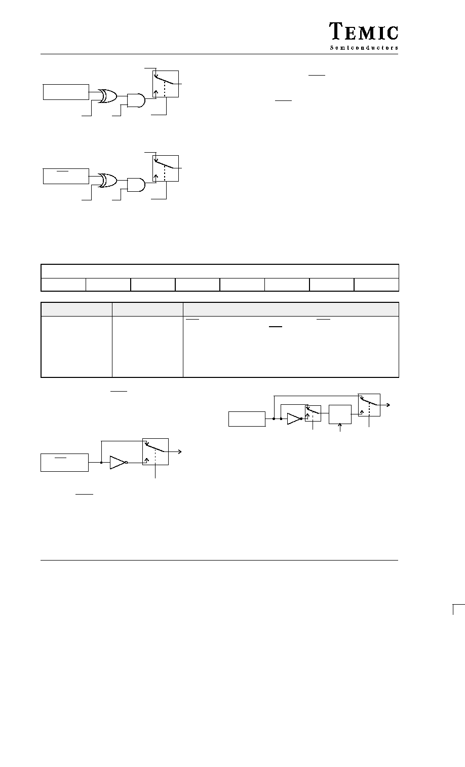
7.4.1. HSYNC and VSYNC Outputs
SOCR is used to configure P3.3 and P3.5 pins as
buffered HSYNC and VSYNC outputs or as general
purpose I/Os. When either HSYNC or VSYNC is
selected, the output level can be respectively
programmed as P3.4 or P3.2 input level (inverted or
not), or as a low level if not enabled. Figure 14. shows
the programmable HSYNC and VSYNC output block
diagram.
SOCR: Synchronisation Output Control Register.
MSB
SFR E5h
LSB
≠
≠
VOS
HOS
VOP
VOE
HOP
HOE
Symbol
Position
Name and Function
HOE
SOCR.0
HSYNC Output Enable bit. Setting this bit enables the HSYNC signal.
HOP
SOCR.1
HSYNC Output Polarity bit. Setting this bit inverts the HSYNC output.
VOE
SOCR.2
VSYNC Output Enable bit. Setting this bit enables the VSYNC signal.
VOP
SOCR.3
VSYNC Output Polarity bit. Setting this bit inverts the VSYNC output.
HOS
SOCR.4
HSYNC Output Selection bit. Setting this bit selects the VSYNC output, clearing it selects
P3.5 SFR bit.
VOS
SOCR.5
VSYNC Output Selection bit. Setting this bit selects the VSYNC output, clearing it selects
P3.3 SFR bit.
CPE
SOCR.6
Clamp Pulse Enable bit. Setting this bit enables the CPO output.
CPP
SOCR.7
Clamp Pulse Polarity bit. Setting this bit selects positive clamp pulses, clearing it selects
negative clamp pulses.
SOCR is a write only register. Its value after reset is 00h
which enables P3.3 and P3.5 general purpose I/O pins.
SOCR is using TSC8051C2 Special Function Register
address, E5h.
TSC8051C2
Rev. A (10 Jan. 97)
18
Preview
MATRA MHS
HOP
PIN
P3.4/T0/HSYNC
P3.5/HOUT
PIN
8051 CORE
P3.5
HOE
HOS
MUX
VOP
PIN
P3.2/INT0/HSYNC
P3.3/VOUT
PIN
8051 CORE
P3.3
VOE
VOS
MUX
Figure 14. Buffered HSYNC and VSYNC block
diagram
7.4.2. HSYNC and VSYNC Inputs
EICON is used to control INT0VSYNC input. Thus, an
interrupt on either falling or rising edge and on either
high or low level can be requested. Figure 15. shows the
programmable INT0/VSYNC input block diagram.
EICON is also used to control T0/HSYNC input as short
pulses input capture to be able to count them with timer
0. Pulse duration shorter than 1 clock period is rejected;
depending on the position of the sampling point in the
pulse, pulse duration longer than 1 clock period and
shorter than 1.5 clock period may be rejected or
accepted; and pulse duration longer than 1.5 clock
period is accepted. Moreover selection of negative or
positive pulses can be programmed.
Accepted pulse is lengthened up to 1 cycle period to be
sampled by the 8051 core (one time per machine cycle:
12 clock periods), this implies that the maximum pulse
frequency is unchanged and equal to f
OSC
/24.
Figure 16. shows the programmable T0/HSYNC input
block diagram. The Digital Timer Delay samples
T0/HSYNC pulses and rejects or lengthens them.
EICON: External Input Control Register
MSB
SFR E4h
LSB
≠
≠
≠
≠
≠
T0L
T0S
I0L
Symbol
Position
Name and Function
I0L
EICON.0
INT0/VSYNC input Level bit. Setting this bit inverts INT0/VSYNC input signal.
Clearing it allows standard use of INT0/VSYNC input.
T0S
EICON.1
T0/HSYNC input Selection bit. Setting this bit allows short pulse capture. Clearing it
allows standard use of T0/HSYNC input.
T0L
EICON.2
T0/HSYNC input Level bit. Setting this bit allows positive pulse capture. Clearing it
allows negative pulse capture.
EICON is a write only register. Its value after reset is 00h
which allows standard INT0 and T0 inputs feature.
EICON is using TSC8051C2 Special Function Register
address, E4h.
INT0
P3.2/INT0/VSYNC
PIN
MUX
I0L
Figure 15. INT0/VSYNC input block diagram
P3.4/T0/HSYNC
Digital
Time
Delay
PIN
T0
MUX
T0S
T0L
f
OSC
Figure 16. T0/HSYNC input block diagram

TSC8051C2
Rev. A (10 Jan. 97)
19
Preview
MATRA MHS
7.4.3. Clamp Pulse Output
The TSC8051C2 provides fully programmable clamp
pulse output to pre≠amplifier IC. User can program a
pulse with positive or negative polarity at either the
falling or rising edge of the HSYNC signal depending on
its polarity.
Figure 17. shows the CPO block diagram. CPE bit in
SOCR is used to configure P1.4 pin as general purpose
I/O or as open drain clamp pulse output, so enables the
CPO. CPP bit in SOCR is used to select the clamp pulse
signal polarity. Depending on the HSYNC polarity
selected by the T0L bit, Clamp pulse is generated on the
falling edge (negative polarity) or on the rising edge
(positive polarity) as shown in Figure 18.
The clamp pulse duration depends on the oscillator
frequency by the following formula:
8051 CORE
P1.4
CPO/P1.4
PIN
F
OSC
Clamp Pulse
Generator
HSYNC
T0L
CPP
CPE
Figure 17. Clamp Pulse Output block diagram
CPO
CPP bit=1
CPO
CPP bit=1
HSYNC
T0L bit=0
HSYNC
T0L bit=1
TCPO
CPO
CPP bit=0
CPO
CPP bit=0
Figure 18. Clamp Pulse Output waveform
T
CPO
+ 1 f
OSC
7.5 " 1 f
OSC
2
(542ns
" 42ns at f
OSC
+ 12 MHz)

TSC8051C2
Rev. A (10 Jan. 97)
20
Preview
MATRA MHS
8. Electrical Characteristics
Absolute Maximum Ratings
(1)
Operating Temperature:
Commercial
0
∞
C to 70
∞
C
. . . . . . . . . . . . . . . . . . . . . . . .
Industrial
≠40
∞
C to +85
∞
C
. . . . . . . . . . . . . . . . . . . . . . .
Storage Temperature
≠65∫C to +150∫C
. . . . . . . . . . . . .
Voltage on VCC to VSS
≠0.5V to +7V
. . . . . . . . . . . . . .
Voltage on Any Pin to VSS
≠0.5V to VCC + 0.5V
. . . .
Power Dissipation
1W
(2)
. . . . . . . . . . . . . . . . . . . . . . . .
Notice:
1. Stresses above those listed under "Absolute Maximum
Ratings" may cause permanent damage to the device. This
is a stress rating only and functional operation of the device
at these or any other conditions above those indicated in the
operational sections of this specification is not implied.
Exposure to absolute maximum rating conditions for
extended periods may affect device reliability.
2. This value is based on the maximum allowable die temperate
and the thermal resistance of the package.
8.1. DC Characteristics
T
A
= 0
∞
C to +70
∞
C; VSS = 0V; VCC = 5V
±
10%; F = 0 to 16MHz.
T
A
= ≠40
∞
C to +85
∞
C; VSS = 0V; VCC = 5V
±
10%; F = 0 to 16MHz.
Symbol
Parameter
Min
Typ
Max
Unit
Test Conditions
Inputs
VIL
Input Low Voltage
≠0.5
0.2 Vcc ≠ 0.1
V
VIH
Input High Voltage except XTAL1, RST
0.2 Vcc + 0.9
Vcc + 0.5
V
VIH1
Input High Voltage, XTAL1, RST
0.7 Vcc
Vcc + 0.5
V
IIL
Logical 0 Input Current ports 1, 2 and 3
≠50
µ
A
Vin = 0.45V
ILI
Input Leakage Current
±
10
µ
A
0.45 < Vin < Vcc
ITL
Logical 1 to 0 Transition Current, ports 1, 2, 3
≠650
µ
A
Vin = 2.0V
VLOW
Power Fail Reset Low Voltage
TBD
3.5
(5)
TBD
V
Outputs
VOL
Output Low Voltage, ports 1, 2, 3,
PWM0≠7
(6)
0.3
0.45
1.0
V
V
V
IOL = 100
µ
A
(4)
IOL = 1.6mA
(4)
IOL = 3.5mA
(4)
VOL1
Output Low Voltage, port 0, ALE, PSEN
(6)
0.3
0.45
1.0
V
V
V
IOL = 200
µ
A
(4)
IOL = 3.2mA
(4)
IOL = 7.0mA
(4)
VOH
Output High Voltage, ports 1, 2, 3
Vcc ≠ 0.3
Vcc ≠ 0.7
Vcc ≠ 1.5
V
V
V
IOH = ≠10
µ
A
IOH = ≠30
µ
A
IOH = ≠60
µ
A
Vcc = 5V
±
10%
VOH1
Output High Voltage, port 0, ALE, PSEN
Vcc ≠ 0.3
Vcc ≠ 0.7
Vcc ≠ 1.5
V
V
V
IOH =≠200
µ
A
IOH = ≠3.2mA
IOH = ≠7.0mA
Vcc = 5V
±
10%
RRST
RST Pulldown Resistor
50
90
(5)
200
k
CIO
Capacitance of I/O Buffer
10
pF
fc = 1MHz, T
A
= 25
∞
C

TSC8051C2
Rev. A (10 Jan. 97)
21
Preview
MATRA MHS
Test Conditions
Unit
Max
Typ
Min
Parameter
Symbol
ICC
Power Supply Current
(7)
Active Mode 12MHz
Idle Mode 12MHz
TBD
TBD
TBD
TBD
mA
mA
Vcc = 5.5V
(1)
Vcc = 5.5V
(2)
IPD
Power Down Current
5
(5)
30
µ
A
Vcc = 2.0V to 5.5V
(3)
Notes for DC Electrical Characteristics
1. ICC is measured with all output pins disconnected; XTAL1 driven
with TCLCH, TCHCL = 5 ns (see Figure 20. ), VIL = VSS +
0.5V, VIH = VCC ≠ 0.5V; XTAL2 N.C.; EA = RST = Port 0 =
VCC. ICC would be slightly higher if a crystal oscillator used
(see Figure 19. ).
2. Idle ICC is measured with all output pins disconnected; XTAL1
driven with TCLCH, TCHCL = 5ns, VIL = VSS + 0.5V, VIH =
VCC≠0.5V; XTAL2 N.C; Port 0 = VCC; EA = RST = VSS (see
Figure 20. ).
3. Power Down ICC is measured with all output pins disconnected;
EA = PORT 0 = VCC; XTAL2 NC.; RST = VSS (see
Figure 21. ).
4. Capacitance loading on Ports 0 and 2 may cause spurious noise
pulses to be superimposed on the VOLs of ALE and Ports 1 and
3. The noise is due to external bus capacitance discharging into
the Port 0 and Port 2 pins when these pins make 1 to 0
transitions during bus operation. In the worst cases (capacitive
loading 100pF), the noise pulse on the ALE line may exceed
0.45V with maxi VOL peak 0.6V. A Schmitt Trigger use is not
necessary.
5. Typicals are based on a limited number of samples and are not
guaranteed. The values listed are at room temperature and 5V.
6. Under steady state (non≠transient) conditions, IOL must be
externally limited as follows:
Maximum IOL per port pin:
10 mA
Maximum IOL per 8≠bit port:
Port 0:
26 mA
Ports 1, 2 and 3:
15 mA
Maximum total IOL for all output pins:
71 mA
If IOL exceeds the test condition, VOL may exceed the related
specification. Pins are not guaranteed to sink current greater than
the listed test conditions.
7. For other values, please contact your sales office.
RST
EA
XTAL2
XTAL1
VSS
VCC
VCC
ICC
(NC)
CLOCK SIGNAL
P0
VCC
VCC
All other pins are disconnected.
Figure 19. ICC Test Condition, Active Mode.
VCC
RST
EA
XTAL2
XTAL1
VSS
VCC
ICC
(NC)
CLOCK SIGNAL
P0
VCC
All other pins are disconnected.
Figure 20. ICC Test Condition, Idle Mode.
VCC
RST
EA
XTAL2
XTAL1
VSS
VCC
ICC
(NC)
P0
VCC
All other pins are disconnected.
Figure 21. ICC Test Condition, Power Down Mode.
TSC8051C2
Rev. A (10 Jan. 97)
22
Preview
MATRA MHS
Vcc≠0.5V
0.45V
0.7Vcc
0.2Vcc≠0.1
TCLCH
TCHCL
TCLCH = TCHCL = 5ns.
Figure 22. Clock Signal Waveform for ICC Tests in Active and Idle Modes.
8.2. Explanation Of The AC Symbol
Each timing symbol has 5 characters. The first character
is always a "T" (stands for time). The other characters,
depending on their positions, stand for the name of a
signal or the logical status of that signal. The following
is a list of all the characters and what they stand for.
Example:
TAVLL = Time for Address Valid to ALE low.
TLLPL = Time for ALE low to PSEN low.
A: Address.
Q: Output data.
C: Clock.
R: READ signal.
D: Input data.
T: Time.
H: Logic level HIGH.
V: Valid.
I: Instruction (Program memory contents).
W: WRITE signal.
L: Logic level LOW, or ALE.
X: No longer a valid logic level.
P: PSEN.
Z: Float.
8.3. AC Parameters
T
A
= 0 to +70
_C; VSS = 0V VCC = 5V
±
10%; 0 to
12MHz
T
A
= ≠40
∞
C to +85
∞
C; VSS = 0V; VCC = 5V
±
10%; F
= 0 to 12MHz.
(Load Capacitance for PORT 0, ALE and PSEN = 100pf;
Load Capacitance for all other outputs = 80 pF.)
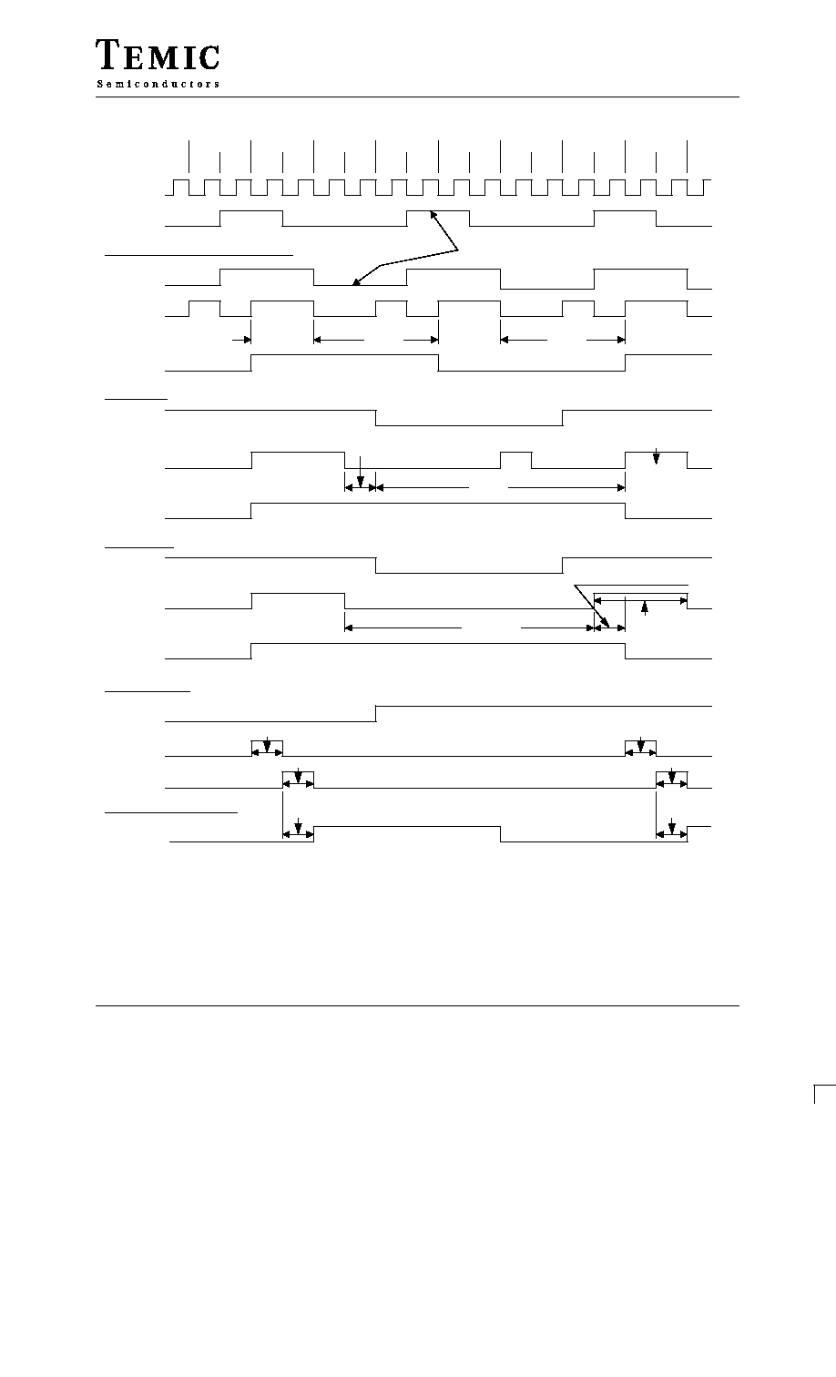
8.4. External Program Memory Characteristics
Symbol
Parameter
0 to 12MHz
Units
Symbol
Parameter
Min
Max
Units
TLHLL
ALE pulse width
2TCLCL ≠ 40
ns
TAVLL
Address Valid to ALE
TCLCL ≠ 40
ns
TLLAX
Address Hold After ALE
TCLCL ≠ 30
ns
TLLIV
ALE to Valid Instruction In
4TCLCL ≠ 100
ns
TLLPL
ALE to PSEN
TCLCL ≠ 30
ns
TPLPH
PSEN Pulse Width
3TCLCL ≠ 45
ns
TPLIV
PSEN to Valid Instruction In
3TCLCL ≠ 105
ns

TSC8051C2
Rev. A (10 Jan. 97)
23
Preview
MATRA MHS
Units
0 to 12MHz
Parameter
Symbol
Units
Max
Min
Parameter
Symbol
TPXIX
Input Instruction Hold After PSEN
0
ns
TPXIZ
Input Instruction Float After PSEN
TCLCL ≠ 25
ns
TPXAV
PSEN to Address Valid
TCLCL ≠ 8
ns
TAVIV
Address to Valid Instruction In
5TCLCL ≠ 105
ns
TPLAZ
PSEN Low to Address Float
10
ns
8.5. External Program Memory Read Cycle
TPLIV
TPLAZ
ALE
PSEN
PORT 0
PORT 2
A0≠A7
A0≠A7
INSTR IN
INSTR IN
INSTR IN
ADDRESS
OR SFR≠P2
ADDRESS A8≠A15
ADDRESS A8≠A15
12 TCLCL
TAVIV
TLHLL
TAVLL
TLLIV
TLLPL
TPLPH
TPXAV
TPXIX
TPXIZ
TLLAX
8.6. External Data Memory Characteristics
Symbol
Parameter
0 to 12MHz
Units
Symbol
Parameter
Min
Max
Units
TRLRH
RD Pulse Width
6TCLCL≠100
ns
TWLWH
WR Pulse Width
6TCLCL≠100
ns
TRLDV
RD to Valid Data In
5TCLCL≠165
ns
TRHDX
Data Hold After RD
0
ns
TRHDZ
Data Float After RD
2TCLCL≠60
ns
TLLDV
ALE to Valid Data In
8TCLCL≠150
ns
TAVDV
Address to Valid Data In
9TCLCL≠165
ns
TLLWL
ALE to WR or RD
3TCLCL≠50
3TCLCL+50
ns
TAVWL
Address to WR or RD
4TCLCL≠130
ns
TQVWX
Data Valid to WR Transition
TCLCL≠50
ns
TQVWH
Data set≠up to WR High
7TCLCL≠150
ns
TWHQX
Data Hold After WR
TCLCL≠50
ns
TRLAZ
RD Low to Address Float
0
ns
TWHLH
RD or WR High to ALE high
TCLCL≠40
TCLCL+40
ns

TSC8051C2
Rev. A (10 Jan. 97)
24
Preview
MATRA MHS
8.7. External Data Memory Write Cycle
TQVWH
TLLAX
ALE
PSEN
WR
PORT 0
PORT 2
A0≠A7
DATA OUT
ADDRESS
OR SFR≠P2
TAVWL
TLLWL
TQVWX
ADDRESS A8≠A15 OR SFR P2
TWHQX
TWHLH
TWLWH
8.8. External Data Memory Read Cycle
ALE
PSEN
RD
PORT 0
PORT 2
A0≠A7
DATA IN
ADDRESS
OR SFR≠P2
TAVWL
TLLWL
TRLAZ
ADDRESS A8≠A15 OR SFR P2
TRHDZ
TWHLH
TRLRH
TLLDV
TRHDX
TAVDV
TLLAX
8.9. Serial Port Timing≠Shift Register Mode
Symbol
Parameter
0 to 12MHz
Units
Symbol
Parameter
Min
Max
Units
TXLXL
Serial port clock cycle time
12TCLCL
ns
TQVHX
Output data set≠up to clock rising edge
10TCLCL≠133
ns
TXHQX
Output data hold after clock rising edge
2TCLCL≠117
ns
TXHDX
Input data hold after clock rising edge
0
ns
TXHDV
Clock rising edge to input data valid
10TCLCL≠133
ns

TSC8051C2
Rev. A (10 Jan. 97)
25
Preview
MATRA MHS
8.10. Shift Register Timing Waveforms
VALID
VALID
INPUT DATA
VALID
VALID
0
1
2
3
4
5
6
8
7
ALE
CLOCK
OUTPUT DATA
WRITE to SBUF
CLEAR RI
TXLXL
TQVXH
TXHQX
TXHDV
TXHDX
SET TI
SET RI
INSTRUCTION
0
1
2
3
4
5
6
7
VALID
VALID
VALID
VALID
8.11. External Clock Drive Characteristics (XTAL1)
Symbol
Parameter
Min
Max
Units
TCLCL
Oscillator Period
83.3
ns
TCHCX
High Time
5
ns
TCLCX
Low Time
5
ns
TCLCH
Rise Time
5
ns
TCHCL
Fall Time
5
ns
8.12. External Clock Drive Waveforms
Vcc≠0.5V
0.45V
0.7Vcc
0.2Vcc≠0.1
TCHCL
TCLCX
TCLCL
TCLCH
TCHCX
8.13. AC Testing Input/Output Waveforms
INPUT/OUTPUT
0.2 Vcc + 0.9
0.2 Vcc ≠ 0.1
Vcc ≠0.5 V
0.45 V
AC inputs during testing are driven at Vcc ≠ 0.5 for a
logic "1" and 0.45V for a logic "0". Timing
measurement are made at VIH min for a logic "1" and
VIL max for a logic "0".

TSC8051C2
Rev. A (10 Jan. 97)
26
Preview
MATRA MHS
8.14. Float Waveforms
FLOAT
FLOAT
VOH ≠ 0.1 V
VOL + 0.1 V
VLOAD
VLOAD + 0.1 V
VLOAD ≠ 0.1 V
For timing purposes as port pin is no longer floating
when a 100 mV change from load voltage occurs and
begins to float when a 100 mV change from the loaded
VOH/VOL level occurs. IOL/IOH
±
20mA.
8.15. Clock Waveform
This diagram indicates when signals are clocked
internally. The time it takes the signals to propagate to
the pins, however, ranges from 25 to 125ns. This
propagation delay is dependent on variables such as
temperature and pin loading. Propagation also varies
from output to output and component. Typically though
(T
A
=25
_C fully loaded) RD and WR propagation delays
are approximately 50ns. The other signals are typically
85ns. Propagation delays are incorporated in the AC
specifications.
TSC8051C2
Rev. A (10 Jan. 97)
27
Preview
MATRA MHS
DATA
PCL OUT
DATA
PCL OUT
DATA
PCL OUT
SAMPLED
SAMPLED
SAMPLED
STATE4
STATE5
STATE6
STATE1
STATE2
STATE3
STATE4
STATE5
P1
P2
P1
P2
P1
P2
P1
P2
P1
P2
P1
P2
P1
P2
P1
P2
FLOAT
FLOAT
FLOAT
THESE SIGNALS ARE NOT ACTIVATED DURING THE
EXECUTION OF A MOVX INSTRUCTION
INDICATES ADDRESS TRANSITIONS
EXTERNAL PROGRAM MEMORY FETCH
FLOAT
DATA
SAMPLED
00H IS EMITTED
DURING THIS PERIOD
DPL OR Rt OUT
INDICATES DPH OR P2 SFR TO PCH TRANSITION
PCL OUT (IF PROGRAM
MEMORY IS EXTERNAL)
PCL OUT (EVEN IF PROGRAM
MEMORY IS INTERNAL)
PCL OUT (IF PROGRAM
MEMORY IS EXTERNAL)
OLD DATA
NEW DATA
P0 PINS SAMPLED
P1, P2, P3 PINS SAMPLED
P1, P2, P3 PINS SAMPLED
P0 PINS SAMPLED
RXD SAMPLED
INTERNAL
CLOCK
XTAL2
ALE
PSEN
P0
P2 (EXT)
READ CYCLE
WRITE CYCLE
RD
P0
P2
WR
PORT OPERATION
MOV PORT SRC
MOV DEST P0
MOV DEST PORT (P1. P2. P3)
(INCLUDES INTO. INT1. TO T1)
SERIAL PORT SHIFT CLOCK
TXD (MODE 0)
DATA OUT
DPL OR Rt OUT
INDICATES DPH OR P2 SFR TO PCH TRANSITION
P0
P2
RXD SAMPLED
TSC8051C2
Rev. A (10 Jan. 97)
28
Preview
MATRA MHS
9. Ordering Information
TSC
51C2
XXX
12
16
Part Number
8051C2: Romless version
51C2: 4Kx8 Mask ROM
TEMIC Semiconductor
Microcontroller Product Line
C
Temperature Range
C : Commercial 0
∞
to 70
∞
C
I : Industrial ≠40
∞
to 85
∞
C
≠12 : 12 MHz version
≠16 : 16 MHz version
Packaging
A : PDIL 40
B : PLCC 44
C : PQFP 44
D : SSOP 44
E : PLCC 52
G : CDIL 40
H : LCC 44
I : CQPJ 44
B
Customer Rom Code
Conditioning
R : Tape & Reel
D : Dry Pack
B : Tape & Reel
and Dry Pack
R
≠A
Bounding Option
≠none : 12 PWM
≠A : 4 PWM & P2x
Examples
Part Number
Description
TSC51C2XXX≠12CA
Mask ROM XXX, 12 MHz, PDIL 40, 0 to 70
∞
C
TSC8051C2≠16CER
ROMless, 16 MHz, PLCC 52, 0 to 70
∞
C, Tape and Reel
Development Tools
Reference
Description
ANM059
Application Note: "How to recognize video mode and generate free running
synchronization signals using TSC8051C1/C2 Microcontroller"
IM≠80C51≠RB≠400≠40
Emulator Base
PC≠TSC8051C1≠RB≠16
Probe card for TSC8051C1. These products are released by Metalink. Please consult the
local tools distributor or your sales office.
Product Marking :
TEMIC
Customer P/N
Temic P/N
©
Intel 80, 82
YYWW Lot Number