 | –≠–ª–µ–∫—Ç—Ä–æ–Ω–Ω—ã–π –∫–æ–º–ø–æ–Ω–µ–Ω—Ç: TSC80C51 | –°–∫–∞—á–∞—Ç—å:  PDF PDF  ZIP ZIP |

TSC80C31/80C51
Rev. E (14 Jan.97)
1
MATRA MHS
Description
The TSC80C31/80C51 is high performance SCMOS
versions of the 8051 NMOS single chip 8 bit
µ
C.
The fully static design of the TSC80C31/80C51 allows to
reduce system power consumption by bringing the clock
frequency down to any value, even DC, without loss of
data.
The TSC80C31/80C51 retains all the features of the 8051
: 4 K bytes of ROM ; 128 bytes of RAM ; 32 I/O lines ;
two 16 bit timers ; a 5-source, 2-level interrupt structure
; a full duplex serial port ; and on-chip oscillator and clock
circuits.
In addition, the TSC80C31/80C51 has two
software-selectable modes of reduced activity for further
reduction in power consumption. In the Idle Mode the
CPU is frozen while the RAM, the timers, the serial port,
and the interrupt system continue to function. In the
Power Down Mode the RAM is saved and all other
functions are inoperative.
The TSC80C31/80C51 is manufactured using SCMOS
process which allows them to run from 0 up to 44 MHz
with VCC = 5 V. The TSC80C31/80C51 is also available
at 20 MHz with 2.7 V < Vcc < 5.5 V.
D TSC80C31/80C51-L16 : Low power version
Vcc : 2.7≠5.5 V
Freq : 0≠16 MHz
D TSC80C31/80C51-L20 : Low power version
Vcc : 2.7≠5.5 V
Freq : 0≠20 MHz
D TSC80C31/80C51-12 : 0 to 12 MHz
D TSC80C31/80C51-20 : 0 to 20 MHz
D TSC80C31/80C51-25 : 0 to 25 MHz
D TSC80C31/80C51-30 : 0 to 30 MHz
D TSC80C31/80C51-36 : 0 to 36 MHz
D TSC80C31/80C51-40 : 0 to 40 MHz
D TSC80C31/80C51-44 : 0 to 44 MHz*
* Commercial and Industrial temperature range only. For other speed
and range please consult your sale office.
Features
D Power control modes
D 128 bytes of RAM
D 4 K bytes of ROM (TSC80C31/80C51)
D 32 programmable I/O lines
D Two 16 bit timer/counter
D 64 K program memory space
D 64 K data memory space
D Fully static design
D 0.8
µ
m CMOS process
D Boolean processor
D 5 interrupt sources
D Programmable serial port
D Temperature range : commercial, industrial, automotive and
military
Optional
D Secret ROM : Encryption
D Secret TAG : Identification number
CMOS 0 to 44 MHz Single-Chip 8 Bit Microcontroller

TSC80C31/80C51
Rev. E (14 Jan.97)
2
MATRA MHS
Interface
Figure 1. Block Diagram

TSC80C31/80C51
Rev. E (14 Jan.97)
3
MATRA MHS
Figure 2. Pin Configuration
Diagrams are for reference only. Packages sizes are not to scale.
P1.4
P1.3
P1.2
P1.1
P1.0
NC
VCC
P0.0/A0
P0.1/A1
P0.2/A2
P0.3/A3
P0.4/A4
P1.5
P1.6
P1.7
RST
RxD/P3.0
NC
TxD/P3.1
INT0/P3.2
INT1/P3.3
T0/P3.4
T1/P3.5
P0.5/A5
P0.6/A6
P0.7/A7
EA
NC
ALE
PSEN
P2.7/A15
P2.6/A14
P2.5/A13
WR/P3.6
RD/P3.7
XT
AL2
XT
AL1
VSS
NC
P2.0/A8
P2.1/A9
P2.2/A10
P2.3/A1
1
P2.4/A12
15
P
16
P
17
P
30
RxD/P
31
TxD/P
32
INT0/P
33
INT1/P
34
T0/P
35
T1/P
36
WR/P
37
RD/P
XT
AL2
XT
AL1
SS
V
NC
20
P
21
P
22
P
23
P
24
P
RST
NC
14
P
13
P
12
P
11
P
10
P
NC
CC
V
00
P
/A8
/A9
/A10
/A1
1
/A12
04
P
/A4
05
P
/A5
06
P
/A6
07
P
/A7
EA
NC
ALE
PSEN
27
P /A15
26
P /A14
25
P /A13
/A0
01
P
/A1
02
P
/A2
03
P
/A3
DIL40
PLCC44
PQFP44

TSC80C31/80C51
Rev. E (14 Jan.97)
4
MATRA MHS
Pin Description
VSS
Circuit ground potential.
VCC
Supply voltage during normal, Idle, and Power Down
operation.
Port 0
Port 0 is an 8 bit open drain bi-directional I/O port. Port 0
pins that have 1's written to them float, and in that state
can be used as high-impedance inputs.
Port 0 is also the multiplexed low-order address and data
bus during accesses to external Program and Data
Memory. In this application it uses strong internal pullups
when emitting 1's. Port 0 also outputs the code bytes
during program verification in the TSC80C31/80C51.
External pullups are required during program
verification. Port 0 can sink eight LS TTL inputs.
Port 1
Port 1 is an 8 bit bi-directional I/O port with internal
pullups. Port 1 pins that have 1's written to them are
pulled high by the internal pullups, and in that state can
be used as inputs. As inputs, Port 1 pins that are externally
being pulled low will source current (IIL, on the data
sheet) because of the internal pullups.
Port 1 also receives the low-order address byte during
program verification. In the TSC80C31/80C51, Port 1
can sink or source three LS TTL inputs. It can drive
CMOS inputs without external pullups.
Port 2
Port 2 is an 8 bit bi-directional I/O port with internal
pullups. Port 2 pins that have 1's written to them are
pulled high by the internal pullups, and in that state can
be used as inputs. As inputs, Port 2 pins that are externally
being pulled low will source current (ILL, on the data
sheet) because of the internal pullups. Port 2 emits the
high-order address byte during fetches from external
Program Memory and during accesses to external Data
Memory that use 16 bit addresses (MOVX @DPTR). In
this application, it uses strong internal pullups when
emitting 1's. During accesses to external Data Memory
that use 8 bit addresses (MOVX @Ri), Port 2 emits the
contents of the P2 Special Function Register.
It also receives the high-order address bits and control
signals during program verification in the
TSC80C31/80C51. Port 2 can sink or source three LS
TTL inputs. It can drive CMOS inputs without external
pullups.
Port 3
Port 3 is an 8 bit bi-directional I/O port with internal
pullups. Port 3 pins that have 1's written to them are
pulled high by the internal pullups, and in that state can
be used as inputs. As inputs, Port 3 pins that are externally
being pulled low will source current (ILL, on the data
sheet) because of the pullups. It also serves the functions
of various special features of the TEMIC C51 Family, as
listed below.
Port Pin
Alternate Function
P3.0
P3.1
P3.2
P3.3
P3.4
P3.5
P3.6
P3.7
RXD (serial input port)
TXD (serial output port)
INT0 (external interrupt 0)
INT1 (external interrupt 1)
TD (Timer 0 external input)
T1 (Timer 1 external input)
WR (external Data Memory write strobe)
RD (external Data Memory read strobe)
Port 3 can sink or source three LS TTL inputs. It can drive
CMOS inputs without external pullups.
RST
A high level on this for two machine cycles while the
oscillator is running resets the device. An internal
pull-down resistor permits Power-On reset using only a
capacitor connected to V
CC
. As soon as the Reset is
applied (Vin), PORT 1, 2 and 3 are tied to one. This
operation is achieved asynchronously even if the
oscillator does not start-up.
ALE
Address Latch Enable output for latching the low byte of
the address during accesses to external memory. ALE is
activated as though for this purpose at a constant rate of
1/6 the oscillator frequency except during an external
data memory access at which time one ALE pulse is
skipped. ALE can sink/source 8 LS TTL inputs. It can
drive CMOS inputs without an external pullup.
If desired, ALE operation can be disabled by setting bit
0 of SFR location AFh (MSCON). With the bit set, ALE
is active only during MOVX instruction and external
fetches. Otherwise the pin is pulled low. MSCON SFR is
set to XXXXXXX0 by reset.
TSC80C31/80C51
Rev. E (14 Jan.97)
5
MATRA MHS
PSEN
Program Store Enable output is the read strobe to external
Program Memory. PSEN is activated twice each machine
cycle during fetches from external Program Memory.
(However, when executing out of external Program
Memory, two activations of PSEN are skipped during
each access to external Data Memory). PSEN is not
activated during fetches from internal Program Memory.
PSEN can sink or source 8 LS TTL inputs. It can drive
CMOS inputs without an external pullup.
EA
When EA is held high, the CPU executes out of internal
Program Memory (unless the Program Counter exceeds
3 FFFH). When EA is held low, the CPU executes only out
of external Program Memory. EA must not be floated.
XTAL1
Input to the inverting amplifier that forms the oscillator.
Receives the external oscillator signal when an external
oscillator is used.
XTAL2
Output of the inverting amplifier that forms the oscillator.
This pin should be floated when an external oscillator is
used.
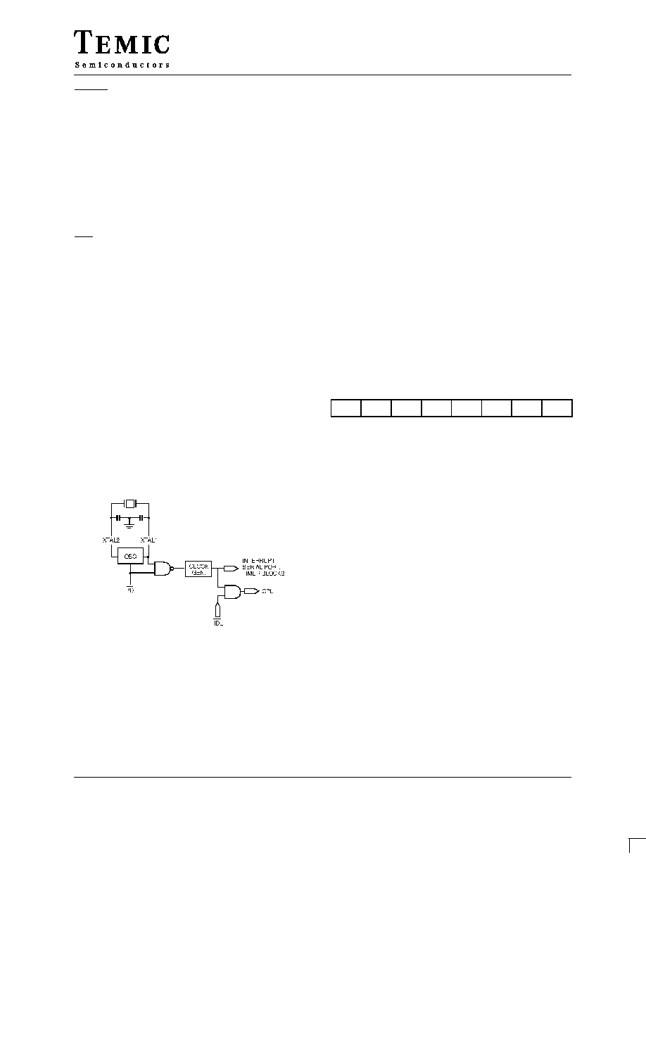
Idle And Power Down Operation
Figure 3. shows the internal Idle and Power Down clock
configuration. As illustrated, Power Down operation
stops the oscillator. Idle mode operation allows the
interrupt, serial port, and timer blocks to continue to
function, while the clock to the CPU is gated off.
These special modes are activated by software via the
Special Function Register, PCON. Its hardware address is
87H. PCON is not bit addressable.
Figure 3. Idle and Power Down Hardware.
PCON : Power Control Register
(MSB)
(LSB)
SMOD
≠
≠
≠
GF1
GF0
PD
IDL
Symbol
Position
Name and Function
SMOD
PCON.7
Double Baud rate bit. When set to
a 1, the baud rate is doubled when
the serial port is being used in
either modes 1, 2 or 3.
≠
PCON.6
(Reserved)
≠
PCON.5
(Reserved)
≠
PCON.4
(Reserved)
GF1
PCON.3
General-purpose flag bit.
GF0
PCON.2
General-purpose flag bit.
PD
PCON.1
Power Down bit. Setting this bit
activates power down operation.
IDL
PCON.0
Idle mode bit. Setting this bit
activates idle mode operation.
If 1's are written to PD and IDL at the same time. PD
takes, precedence. The reset value of PCON is
(000X0000).
Idle Mode
The instruction that sets PCON.0 is the last instruction
executed before the Idle mode is activated. Once in the
Idle mode the CPU status is preserved in its entirety : the
Stack Pointer, Program Counter, Program Status Word,
Accumulator, RAM and all other registers maintain their
data during idle. Table 1 describes the status of the
external pins during Idle mode.
There are three ways to terminate the Idle mode.
Activation of any enabled interrupt will cause PCON.0 to
be cleared by hardware, terminating Idle mode. The
interrupt is serviced, and following RETI, the next
instruction to be executed will be the one following the
instruction that wrote 1 to PCON.0.
TSC80C31/80C51
Rev. E (14 Jan.97)
6
MATRA MHS
The flag bits GF0 and GF1 may be used to determine
whether the interrupt was received during normal
execution or during the Idle mode. For example, the
instruction that writes to PCON.0 can also set or clear one
or both flag bits. When Idle mode is terminated by an
enabled interrupt, the service routine can examine the
status of the flag bits.
The second way of terminating the Idle mode is with a
hardware reset. Since the oscillator is still running, the
hardware reset needs to be active for only 2 machine
cycles (24 oscillator periods) to complete the reset
operation.
Power Down Mode
The instruction that sets PCON.1 is the last executed prior
to entering power down. Once in power down, the
oscillator is stopped. The contents of the onchip RAM and
the Special Function Register is saved during power down
mode. The hardware reset initiates the Special Fucntion
Register. In the Power Down mode, VCC may be lowered
to mi-nimize circuit power consumption. Care must be
taken to ensure the voltage is not reduced until the power
down mode is entered, and that the voltage is restored
before the hardware reset is applied which freezes the
oscillator. Reset should not be released until the oscillator
has restarted and stabilized. A hardware reset is the only
way of exiting the power down mode.
Table 1 describes the status of the external pins while in
the power down mode. It should be noted that if the power
down mode is activated while in external program
memory, the port data that is held in the Special Function
Register P2 is restored to Port 2. If the data is a 1, the port
pin is held high during the power down mode by the
strong pullup, T1, shown in Figure 4.
Table 1. Status of the external pins during idle and power down modes.
MODE
PROGRAM MEMORY
ALE
PSEN
PORT0
PORT1
PORT2
PORT3
Idle
Internal
1
1
Port Data
Port Data
Port Data
Port Data
Idle
External
1
1
Floating
Port Data
Address
Port Data
Power Down
Internal
0
0
Port Data
Port Data
Port Data
Port Data
Power Down
External
0
0
Floating
Port Data
Port Data
Port Data
Stop Clock Mode
Due to static design, the TSC80C31/80C51 clock speed
can be reduced until 0 MHz without any data loss in
memory or registers. This mode allows step by step
utilization, and permits to reduce system power
consumption by bringing the clock frequency down to
any value. At 0 MHz, the power consumption is the same
as in the Power Down Mode.
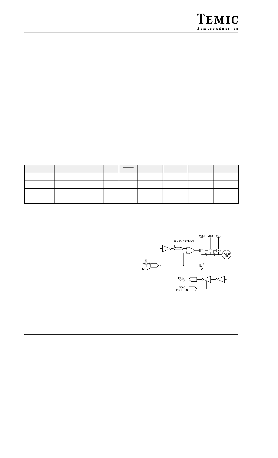
I/O Ports
The I/O buffers for Ports 1, 2 and 3 are implemented as
shown in Figure 4.
Figure 4. I/O Buffers in the TSC80C31/80C51 (Ports
1, 2, 3).
TSC80C31/80C51
Rev. E (14 Jan.97)
7
MATRA MHS
When the port latch contains a 0, all pFETS in Figure 4.
are off while the nFET is turned on. When the port latch
makes a 0-to-1 transition, the nFET turns off. The strong
pFET, T1, turns on for two oscillator periods, pulling the
output high very rapidly. As the output line is drawn high,
pFET T3 turns on through the inverter to supply the IOH
source current. This inverter and T form a latch which
holds the 1 and is supported by T2.
When Port 2 is used as an address port, for access to
external program of data memory, any address bit that
contains a 1 will have his strong pullup turned on for the
entire duration of the external memory access.
When an I/O pin son Ports 1, 2, or 3 is used as an input,
the user should be aware that the external circuit must
sink current during the logical 1-to-0 transition. The
maximum sink current is specified as ITL under the D.C.
Specifications. When the input goes below
approximately 2 V, T3 turns off to save ICC current. Note,
when returning to a logical 1, T2 is the only internal
pullup that is on. This will result in a slow rise time if the
user's circuit does not force the input line high.
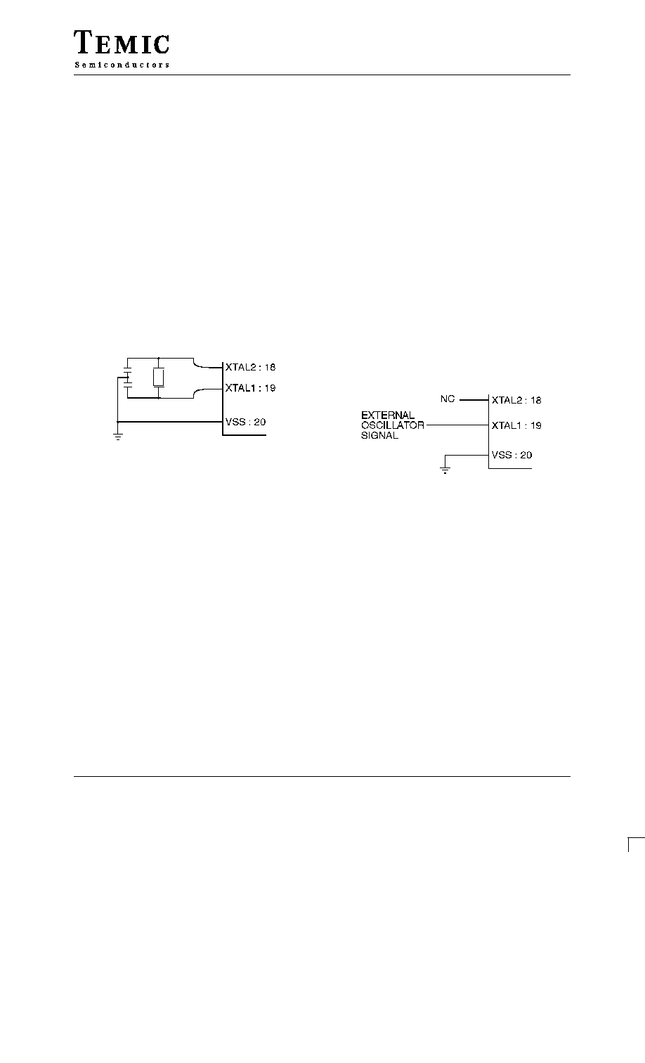
Oscillator Characteristics
XTAL1 and XTAL2 are the input and output respectively,
of an inverting amplifier which is configured for use as an
on-chip oscillator, as shown in Figure 5. Either a quartz
crystal or ceramic resonator may be used.
Figure 5. Crystal Oscillator.
To drive the device from an external clock source,
XTAL1 should be driven while XTAL2 is left
unconnected as shown in Figure 6. There are no
requirements on the duty cycle of the external clock
signal, since the input to the internal clocking circuitry is
through a divide-by-two flip-flop, but minimum and
maximum high and low times specified on the Data Sheet
must be observed.
Figure 6. External Drive Configuration.
TSC80C51 with Secret ROM
TEMIC offers TSC80C31/80C51 with the encrypted
secret ROM option to secure the ROM code contained in
the TSC80C31/80C51 microcontrollers.
The clear reading of the program contained in the ROM
is made impossible due to an encryption through several
random keys implemented during the manufacturing
process.
The keys used to do such encryption are selected
randomwise and are definitely different from one
microcontroller to another.
This encryption is activated during the following phases :
≠
Everytime a byte is addressed during a verify of the
ROM content, a byte of the encryption array is
selected.
≠
MOVC instructions executed from external program
memory are disabled when fetching code bytes from
internal memory.
≠
EA is sampled and latched on reset, thus all state
modification are disabled.
For further information please refer to the application
note (ANM053) available upon request.

TSC80C31/80C51
Rev. E (14 Jan.97)
8
MATRA MHS
TSC80C31/80C51 with Secret TAG
TEMIC offers special 64-bit identifier called "SECRET
TAG" on the microcontroller chip.
The Secret Tag option is available on both ROMless and
masked microcontrollers.
The Secret Tag feature allows serialization of each
microcontroller for identification of a specific
equipment. A unique number per device is implemented
in the chip during manufacturing process. The serial
number is a 64-bit binary value which is contained and
addressable in the Special Function Registers (SFR) area.
This Secret Tag option can be read-out by a software
routine and thus enables the user to do an individual
identity check per device. This routine is implemented
inside the microcontroller ROM memory in case of
masked version which can be kept secret (and then the
value of the Secret Tag also) by using a ROM Encryption.
For further information, please refer to the application
note (ANM031) available upon request.
TSC80C31/80C51
Rev. E (14 Jan.97)
9
MATRA MHS
Electrical Characteristics
Absolute Maximum Ratings*
Ambiant Temperature Under Bias :
C = commercial
0
∞
C to 70
∞
C
. . . . . . . . . . . . . . . . . . . . . . . . . . . . . . . .
I = industrial
≠40
∞
C to 85
∞
C
. . . . . . . . . . . . . . . . . . . . . . . . . . . . . . . . .
Storage Temperature
≠65
∞
C to + 150
∞
C
. . . . . . . . . . . . . . . . . . . . . . . .
Voltage on VCC to VSS
≠0.5 V to + 7 V
. . . . . . . . . . . . . . . . . . . . . . . .
Voltage on Any Pin to VSS
≠0.5 V to V
CC
+ 0.5 V
. . . . . . . . . . . . . . . . . . .
Power Dissipation
1 W**
. . . . . . . . . . . . . . . . . . . . . . . . . . . . . . . . . . .
** This value is based on the maximum allowable die temperature and
the thermal resistance of the package
* Notice
Stresses at or above those listed under " Absolute Maximum Ratings"
may cause permanent damage to the device. This is a stress rating only
and functional operation of the device at these or any other conditions
above those indicated in the operational sections of this specification is
not implied. Exposure to absolute maximum rating conditions may affect
device reliability.
DC Parameters
TA = 0
∞
C to 70
∞
C ; VSS = 0 V ; VCC = 5 V
±
10 % ; F = 0 to 44 MHz
TA = ≠40
∞
C + 85
∞
C ; VSS = 0 V ; VCC = 5 V
±
10 % ; F = 0 to 44 MHz
Symbol
Parameter
Min
Typ (3)
Max
Unit
Test Conditions
VIL
Input Low Voltage
≠ 0.5
0.2 Vcc ≠ 0.1
V
VIH
Input High Voltage (Except XTAL and RST)
0.2 Vcc + 0.9
Vcc + 0.5
V
VIH1
Input High Voltage (for XTAL and RST)
0.7 Vcc
Vcc + 0.5
V
VOL
Output Low Voltage (Port 1, 2 and 3) (4)
0.3
0.45
1.0
V
V
V
IOL = 100
µ
A
IOL = 1.6 mA (2)
IOL = 3.5 mA
VOL1
Output Low Voltage (Port 0, ALE, PSEN) (4)
0.3
0.45
1.0
V
V
V
IOL = 200
µ
A
IOL = 3.2 mA (2)
IOL = 7.0 mA
VOH
Output High Voltage Port 1, 2, 3
Vcc ≠ 0.3
V
IOH = ≠ 10
µ
A
Vcc ≠ 0.7
V
IOH = ≠ 30
µ
A
Vcc ≠ 1.5
V
IOH = ≠ 60
µ
A
VCC = 5 V
±
10 %
VOH1
Output High Voltage (Port 0, ALE, PSEN)
Vcc ≠ 0.3
V
IOH = ≠ 200
µ
A
Vcc ≠ 0.7
V
IOH = ≠ 3.2 mA
Vcc ≠ 1.5
V
IOH = ≠ 7.0 mA
VCC = 5 V
±
10 %
IIL
Logical 0 Input Current (Ports 1, 2 and 3)
≠ 50
µ
A
Vin = 0.45 V
ILI
Input leakage Current
±
10
µ
A
0.45 < Vin < Vcc
ITL
Logical 1 to 0 Transition Current (Ports 1, 2 and 3)
≠ 650
µ
A
Vin = 2.0 V
IPD
Power Down Current
5
30
µ
A
Vcc = 2.0 V to 5.5 V (1)
RRST
RST Pulldown Resistor
50
90
200
K
W
CIO
Capacitance of I/O Buffer
10
pF
fc = 1 MHz, Ta = 25
_C
ICC
Power Supply Current
Freq = 1 MHz
Icc op
Icc idle
Freq = 6 MHz
Icc op
Icc idle
Freq
12 MHz Icc op max = 0.9 Freq (MHz) + 5
0.7
0.5
4.2
1.4
1.8
1
9
3.5
mA
mA
mA
mA
mA
Vcc = 5.5 V
Freq
12 MHz Icc op max = 0.9 Freq (MHz) + 5
Icc idle max = 0.3 Freq (MHz) + 1.7
Freq
20 MHz Icc op typ = 0.7 Freq (MHz)
Freq
20 MHz Icc op typ = 0.5 Freq (MHz) + 4
Freq
20 MHz Icc idle typ = 0.16 Freq (MHz) + 0.4
Freq
20 MHz Icc idle typ = 0.12 Freq (MHz) + 1.2
mA
mA
mA
mA
mA
mA

TSC80C31/80C51
Rev. E (14 Jan.97)
10
MATRA MHS
Absolute Maximum Ratings*
Ambient Temperature Under Bias :
A = Automotive
≠40
∞
C to +125
∞
C
. . . . . . . . . . . . . . . . . . . . . . . . . . . .
Storage Temperature
≠65
∞
C to + 150
∞
C
. . . . . . . . . . . . . . . . . . . . . . . .
Voltage on VCC to VSS
≠0.5 V to + 7 V
. . . . . . . . . . . . . . . . . . . . . . . .
Voltage on Any Pin to VSS
≠0.5 V to VCC + 0.5 V
. . . . . . . . . . . . . . .
Power Dissipation
1 W**
. . . . . . . . . . . . . . . . . . . . . . . . . . . . . . . . . . .
** This value is based on the maximum allowable die temperature and
the thermal resistance of the package
* Notice
Stresses above those listed under " Absolute Maximum Ratings" may
cause permanent damage to the device. This is a stress rating only and
functional operation of the device at these or any other conditions above
those indicated in the operational sections of this specification is not
implied. Exposure to absolute maximum rating conditions for extended
periods may affect device reliability.
DC Parameters
TA = ≠40
∞
C + 125
∞
C ; VSS = 0 V ; VCC = 5 V
±
10 % ; F = 0 to 40 MHz
Symbol
Parameter
Min
Typ (3)
Max
Unit
Test Conditions
VIL
Input Low Voltage
≠ 0.5
0.2 Vcc ≠ 0.1
V
VIH
Input High Voltage (Except XTAL and RST)
0.2 Vcc + 0.9
Vcc + 0.5
V
VIH1
Input High Voltage (for XTAL and RST)
0.7 Vcc
Vcc + 0.5
V
VOL
Output Low Voltage (Port 1, 2 and 3) (4)
0.3
0.45
1.0
V
V
V
IOL = 100
µ
A
IOL = 1.6 mA (2)
IOL = 3.5 mA
VOL1
Output Low Voltage (Port 0, ALE, PSEN) (4)
0.3
0.45
1.0
V
V
V
IOL = 200
µ
A
IOL = 3.2 mA (2)
IOL = 7.0 mA
VOH
Output High Voltage Port 1, 2 and 3
Vcc ≠ 0.3
V
IOH = ≠ 10
µ
A
Vcc ≠ 0.7
V
IOH = ≠ 30
µ
A
Vcc ≠ 1.5
V
IOH = ≠ 60
µ
A
VCC = 5 V
±
10 %
VOH1
Output High Voltage (Port 0, ALE, PSEN)
Vcc ≠ 0.3
V
IOH = ≠ 200
µ
A
Vcc ≠ 0.7
V
IOH = ≠ 3.2 mA
Vcc ≠ 1.5
V
IOH = ≠ 7.0 mA
VCC = 5 V
±
10 %
IIL
Logical 0 Input Current (Ports 1, 2 and 3)
≠ 75
µ
A
Vin = 0.45 V
ILI
Input leakage Current
±
10
µ
A
0.45 < Vin < Vcc
ITL
Logical 1 to 0 Transition Current (Ports 1, 2 and 3)
≠ 750
µ
A
Vin = 2.0 V
IPD
Power Down Current
5
75
µ
A
Vcc = 2.0 V to 5.5 V (1)
RRST
RST Pulldown Resistor
50
90
200
K
W
CIO
Capacitance of I/O Buffer
10
pF
fc = 1 MHz, Ta = 25
_C
ICC
Power Supply Current
Freq = 1 MHz
Icc op
Icc idle
Freq = 6 MHz
Icc op
Icc idle
Freq
12 MHz Icc op max = 0.9 Freq (MHz) + 5
0.7
0.5
4.2
1.4
1.8
1
9
3.5
mA
mA
mA
mA
mA
Vcc = 5.5 V
Freq
12 MHz Icc op max = 0.9 Freq (MHz) + 5
Icc idle max = 0.3 Freq (MHz) + 1.7
Freq
20 MHz Icc op typ = 0.7 Freq (MHz)
Freq
20 MHz Icc op typ = 0.5 Freq (MHz) + 4
Freq
20 MHz Icc idle typ = 0.16 Freq (MHz) + 0.4
Freq
20 MHz Icc idle typ = 0.12 Freq (MHz) + 1.2
mA
mA
mA
mA
mA
mA
TSC80C31/80C51
Rev. E (14 Jan.97)
11
MATRA MHS
Absolute Maximum Ratings*
Ambient Temperature Under Bias :
M = Military
≠55
∞
C to +125
∞
C
. . . . . . . . . . . . . . . . . . . . . . . . . . . . . . .
Storage Temperature
≠65
∞
C to + 150
∞
C
. . . . . . . . . . . . . . . . . . . . . . . .
Voltage on VCC to VSS
≠0.5 V to + 7 V
. . . . . . . . . . . . . . . . . . . . . . . .
Voltage on Any Pin to VSS
≠0.5 V to VCC + 0.5 V
. . . . . . . . . . . . . . .
Power Dissipation
1 W**
. . . . . . . . . . . . . . . . . . . . . . . . . . . . . . . . . . .
** This value is based on the maximum allowable die temperature and
the thermal resistance of the package
* Notice
Stresses at or above those listed under " Absolute Maximum Ratings"
may cause permanent damage to the device. This is a stress rating only
and functional operation of the device at these or any other conditions
above those indicated in the operational sections of this specification is
not implied. Exposure to absolute maximum rating conditions may affect
device reliability.
DC Parameters
TA = ≠55
∞
C + 125
∞
C ; Vss = 0 V ; Vcc = 5 V
±
10 % ; F = 0 to 40 MHz
Symbol
Parameter
Min
Typ (3)
Max
Unit
Test Conditions
VIL
Input Low Voltage
≠ 0.5
0.2 Vcc ≠ 0.1
V
VIH
Input High Voltage (Except XTAL and RST)
0.2 Vcc + 0.9
Vcc + 0.5
V
VIH1
Input High Voltage (for XTAL and RST)
0.7 Vcc
Vcc + 0.5
V
VOL
Output Low Voltage (Port 1, 2 and 3) (4)
0.45
V
IOL = 1.6 mA (2)
VOL1
Output Low Voltage (Port 0, ALE, PSEN) (4)
0.45
V
IOL = 3.2 mA (2)
VOH
Output High Voltage (Port 1, 2 and 3)
2.4
V
IOH = ≠ 60
µ
A
Vcc = 5 V
±
10 %
0.75 Vcc
V
IOH = ≠ 25
µ
A
0.9 Vcc
V
IOH = ≠ 10
µ
A
VOH1
Output High Voltage
(Port 0 in External Bus Mode, ALE, PEN)
2.4
V
IOH = ≠ 400
µ
A
Vcc = 5 V
±
10 %
0.75 Vcc
V
IOH = ≠ 150
µ
A
0.9 Vcc
V
IOH = ≠ 40
µ
A
IIL
Logical 0 Input Current (Ports 1, 2 and 3)
≠ 75
µ
A
Vin = 0.45 V
ILI
Input leakage Current
+/≠ 10
µ
A
0.45 < Vin < Vcc
ITL
Logical 1 to 0 Transition Current (Ports 1, 2 and 3)
≠ 750
µ
A
Vin = 2.0 V
IPD
Power Down Current
5
75
µ
A
Vcc = 2.0 V to 5.5 V (1)
RRST
RST Pulldown Resistor
50
90
200
K
CIO
Capacitance of I/O Buffer
10
pF
fc = 1 MHz, Ta = 25
_C
ICC
Power Supply Current
Freq = 1 MHz
Icc op
Icc idle
Freq = 6 MHz
Icc op
Icc idle
Freq
12 MHz Icc op max = 0.9 Freq (MHz) + 5
0.7
0.5
4.2
1.4
1.8
1
9
3.5
mA
mA
mA
mA
mA
Vcc = 5.5 V
Freq
12 MHz Icc op max = 0.9 Freq (MHz) + 5
Icc idle max = 0.3 Freq (MHz) + 1.7
Freq
20 MHz Icc op typ = 0.7 Freq (MHz)
Freq
20 MHz Icc op typ = 0.5 Freq (MHz) + 4
Freq
20 MHz Icc idle typ = 0.16 Freq (MHz) + 0.4
Freq
20 MHz Icc idle typ = 0.12 Freq (MHz) + 1.2
mA
mA
mA
mA
mA
mA
TSC80C31/80C51
Rev. E (14 Jan.97)
12
MATRA MHS
Absolute Maximum Ratings*
Ambient Temperature Under Bias :
C = Commercial
0
∞
C to 70
∞
C
. . . . . . . . . . . . . . . . . . . . . . . . . . . . . . . .
I = Industrial
≠40
∞
C to 85
∞
C
. . . . . . . . . . . . . . . . . . . . . . . . . . . . . . . . .
Storage Temperature
≠65
∞
C to + 150
∞
C
. . . . . . . . . . . . . . . . . . . . . . . .
Voltage on VCC to VSS
≠0.5 V to + 7 V
. . . . . . . . . . . . . . . . . . . . . . . .
Voltage on Any Pin to VSS
≠0.5 V to VCC + 0.5 V
. . . . . . . . . . . . . . .
Power Dissipation
1 W**
. . . . . . . . . . . . . . . . . . . . . . . . . . . . . . . . . . .
** This value is based on the maximum allowable die temperature and
the thermal resistance of the package
* Notice
Stresses at or above those listed under " Absolute Maximum Ratings"
may cause permanent damage to the device. This is a stress rating only
and functional operation of the device at these or any other conditions
above those indicated in the operational sections of this specification is
not implied. Exposure to absolute maximum rating conditions may affect
device reliability.
DC Characteristics : Low Power Version
TA = 0
∞
C to 70
∞
C ; Vcc = 2.7 V to 5.5 V ; Vss = 0 V ; F = 0 to 20 MHz
TA = ≠40
∞
C to 85
∞
C ; Vcc = 2.7 V to 5.5 V ; F = 0 to 20 MHz
Symbol
Parameter
Min
Typ (3)
Max
Unit
Test Conditions
VIL
Input Low Voltage
≠ 0.5
0.2 V
CC
≠ 0.1
V
VIH
Input High Voltage (Except XTAL and RST)
0.2 V
CC
+ 0.9
V
CC
+ 0.5
V
VIH2
Input High Voltage to RST for Reset
0.7 V
CC
V
CC
+ 0.5
V
VIH1
Input High Voltage to XTAL1
0.7 V
CC
V
CC
+ 0.5
V
VPD
Power Down Voltage to Vcc in PD Mode
2.0
5.5
V
VOL
Output Low Voltage (Ports 1, 2, 3) (4)
0.45
V
IOL = 0.8 mA (2)
VOL1
Output Low Voltage Port 0, ALE, PSEN (4)
0.45
V
IOL = 1.6 mA (2)
VOH
Output High Voltage (Port 1, 2 and 3)
0.9 Vcc
V
IOH = ≠ 10
µ
A
VOH1
Output High Voltage (Port 0 in External Bus Mode),
ALE, PSEN
0.9 Vcc
V
IOH = ≠ 40
µ
A
IIL
Logical 0 Input Current Ports 1, 2, 3
≠ 50
µ
A
Vin = 0.45 V
ILI
Input Leakage Current
±
10
µ
A
0.45 < Vin < V
CC
ITL
Logical 1 to 0 Transition Current (Ports 1, 2, 3)
≠ 650
µ
A
Vin = 2.0 V
IPD
Power Down Current
5
30
µ
A
V
CC
= 2.0 V to 5.5 V
(1)
RRST
RST Pulldown Resistor
50
90
200
k
CIO
Capacitance of I/O Buffer
10
pF
fc = 1 MHz, T
A
= 25
_C
Icc (mA)
Operating (1)
Idle (1)
Frequency/Vcc
2.7 V
3 V
3.3 V
2.7 V
3 V
3.3 V
Max
Typ
Max
Typ
Max
Typ
Max
Typ
Max
Typ
Max
Typ
1 MHz
0.8
0.37
1
0.42
1.1
0.46
0.4
0.22
0.5
0.24
0.6
0.27
6 MHz
4
2.2
5
2.5
6
2.7
1.5
1.2
1.7
1.4
2
1.6
12 MHz
8
4
10
4.7
12
5.3
2.5
1.7
3
2.2
3.5
2.6
16 MHz
10
5
12
5.8
14
6.6
3
1.9
3.8
2.5
4.5
3
Freq > 12MHz (Vcc = 5.5 V)
Icc op max (mA) = 0.9
◊
Freq (MHz) + 5
Icc Idle max (mA) = 0.3
◊
Freq (MHz) + 1.7
TSC80C31/80C51
Rev. E (14 Jan.97)
13
MATRA MHS
Idle ICC is measured with all output pins disconnected ;
XTAL1 driven with TCLCH, TCHCL = 5 ns, VIL =
VSS + 0.5 V, VIH = VCC ≠ 0.5 V ; XTAL2 N.C ; Port 0 =
VCC ; EA = RST = VSS.
Power Down ICC is measured with all output pins
disconnected ; EA = PORT 0 = VCC ; XTAL2 N.C. ;
RST = VSS.
Note 2 : Capacitance loading on Ports 0 and 2 may cause
spurious noise pulses to be superimposed on the VOLS of
ALE and Ports 1 and 3. The noise is due to external bus
capacitance discharging into the Port 0 and Port 2 pins
when these pins make 1 to 0 transitions during bus
operations. In the worst cases (capacitive loading 100
pF), the noise pulse on the ALE line may exceed 0.45 V
with maxi VOL peak 0.6 V. A Schmitt Trigger use is not
necessary.
Note 3 : Typicals are based on a limited number of
samples and are not guaranteed. the values listed are at
room temperature and 5V.
Note 4 : Under steady state (non≠transient)) conditions,
IOL must be externally limited as follows :
Maximum IOL per port pin :
10 mA
Maximum IOL per 8≠bit port :
Port 0 :
26 mA
Ports 1, 2 and 3 :
15 mA
Maximum total IOL for all output pins :
71 mA
If IOL exceed the test condition, VOL may exceed the
related specification. Pins are not guaranteed to sink
current greater than the listed test conditions.
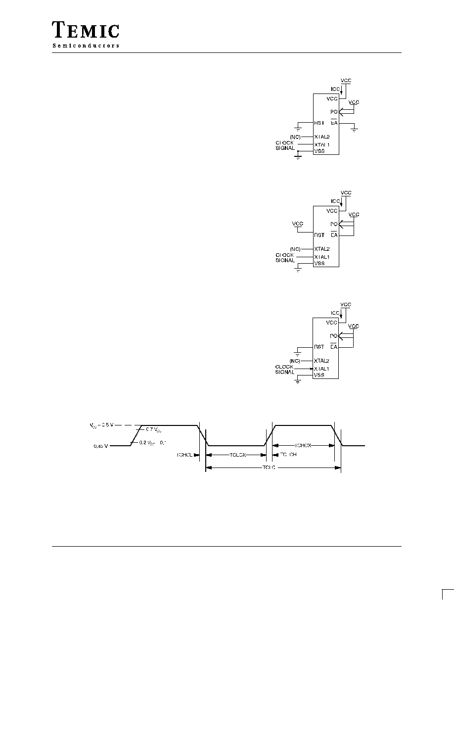
Figure 7. ICC Test Condition, Idle Mode.
All other pins are disconnected.
Figure 8. ICC Test Condition, Active Mode.
All other pins are disconnected.
Figure 9. ICC Test Condition, Power Down Mode.
All other pins are disconnected.
Figure 10. Clock Signal Waveform for ICC Tests in Active and Idle Modes.
TCLCH = TCHCL = 5 ns.
TSC80C31/80C51
Rev. E (14 Jan.97)
14
MATRA MHS
Explanation of the AC Symbol
Each timing symbol has 5 characters. The first character
is always a "T" (stands for time). The other characters,
depending on their positions, stand for the name of a
signal or the logical status of that signal. The following
is a list of all the characters and what they stand for.
Example :
TAVLL = Time for Address Valid to ALE low.
TLLPL = Time for ALE low to PSEN low.
A : Address.
C : Clock.
D : Input data.
H : Logic level HIGH
I : Instruction (program memory contents).
L : Logic level LOW, or ALE.
P : PSEN.
Q : Output data.
R : READ signal.
T : Time.
V : Valid.
W : WRITE signal.
X : No longer a valid logic level.
Z : Float.
AC Parameters
TA= 0 to + 70
∞
C ; Vss= 0 V ; Vcc= 5 V
±
10 % ; F= 0 to 44 MHz
TA= 0 to +70
∞
C ; Vss= 0 V ; 2.7 V <Vcc < 5.5 V ; F= 0 to 16 MHz
TA=≠40
∞
to +85
∞
C; Vss= 0 V; 2.7 V<Vcc <5.5 V ; F= 0 to 16 MHz
TA= ≠55
∞
+ 125
∞
C; Vss= 0 V; Vcc= 5 V
±
10 % ; F= 0 to 40 MHz
(Load Capacitance for PORT 0, ALE and PSEN = 100 pF ; Load
Capacitance for all other outputs = 80 pF)
External Program Memory Characteristics (values in ns)
16 MHz
20 MHz
25 MHz
30 MHz
36 MHz
40 MHz
44 MHz
SYMBOL
PARAMETER
min max min max min max min max min max min max min max
TLHLL
ALE Pulse Width
110
90
70
60
50
40
30
TAVLL
Address valid to ALE
40
30
20
15
10
9
7
TLLAX
Address Hold After ALE
35
35
35
35
35
30
20
TLLIV
ALE to valid instr in
185
170
130
100
80
70
65
TLLPL
ALE to PSEN
45
40
30
25
20
15
12
TPLPH
PSEN pulse Width
165
130
100
80
75
65
54
TPLIV
PSEN to valid instr in
125
110
85
65
50
45
35
TPXIX
Input instr Hold After PSEN
0
0
0
0
0
0
0
TPXIZ
Input instr Float After PSEN
50
45
35
30
25
20
10
TPXAV
PSEN to Address Valid
55
50
40
35
30
25
15
TAVIV
Address to Valid instr in
230
210
170
130
90
80
70
TPLAZ
PSEN low to Address Float
10
10
8
6
5
5
5
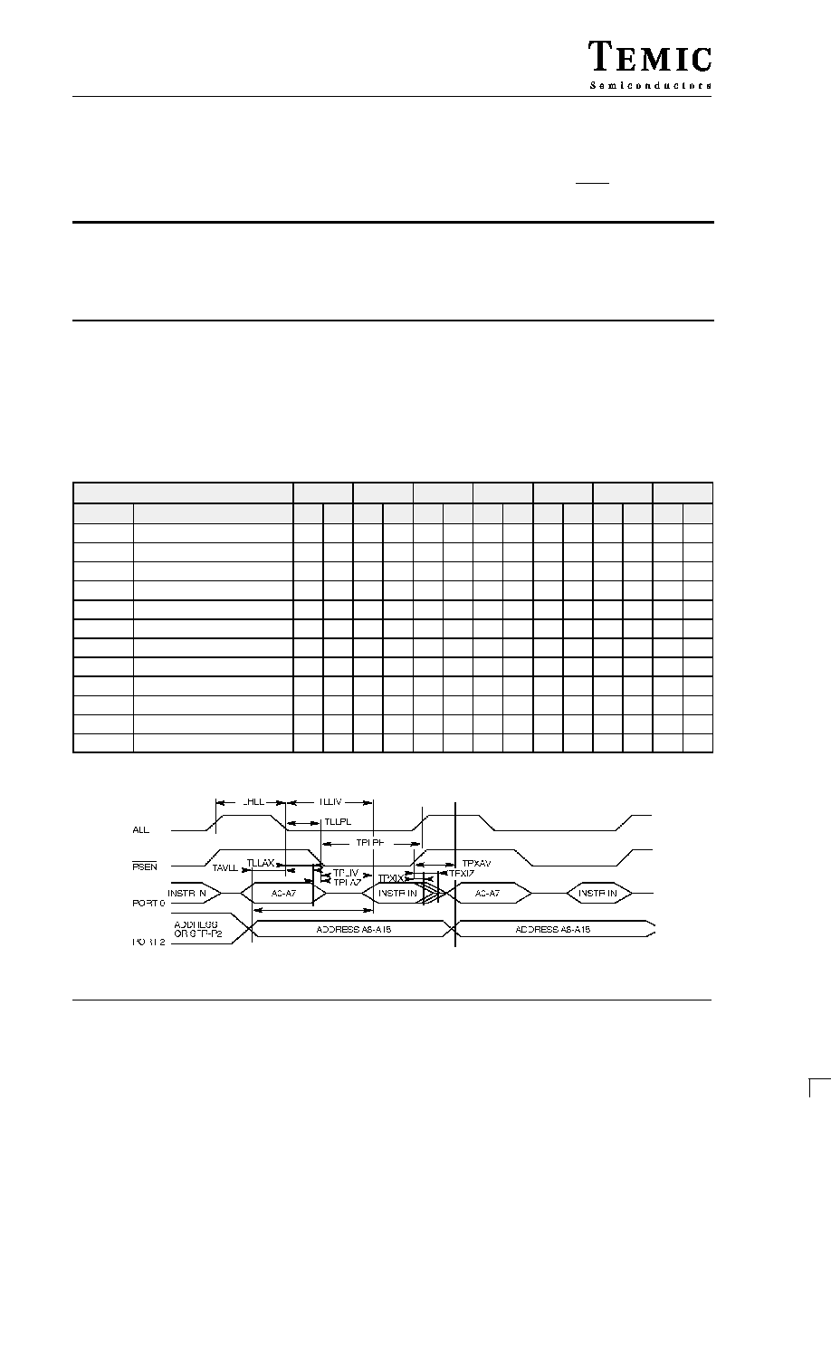
External Program Memory Read Cycle
TAVIV
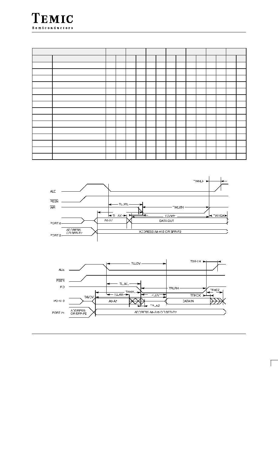
TSC80C31/80C51
Rev. E (14 Jan.97)
15
MATRA MHS
External Data Memory Characteristics (values in ns)
16 MHz
20 MHz
25 MHz
30 MHz
36 MHz
40 MHz
44 MHz
SYMBOL
PARAMETER
min max min max min max min max min max min max min max
TRLRH
RD pulse Width
340
270
210
180
120
100
80
TWLWH
WR pulse Width
340
270
210
180
120
100
80
TLLAX
Address Hold After ALE
85
85
70
55
35
30
25
TRLDV
RD to Valid data in
240
210
175
135
110
90
70
TRHDX
Data hold after RD
0
0
0
0
0
0
0
TRHDZ
Data float after RD
90
90
80
70
50
45
35
TLLDV
ALE to Valid Data In
435
370
350
235
170
150
130
TAVDV
Address to Valid Data IN
480
400
300
260
190
180
170
TLLWL
ALE to WR or RD
150
250
135
170
120
130
90
115
70
100
60
95
50
85
TAVWL
Address to WR or RD
180
180
140
115
75
65
55
TQVWX
Data valid to WR transition
35
35
30
20
15
10
6
TQVWH
Data Setup to WR transition
380
325
250
215
170
160
140
TWHQX
Data Hold after WR
40
35
30
20
15
10
6
TRLAZ
RD low to Address Float
0
0
0
0
0
0
0
TWHLH
RD or WR high to ALE high
35
90
35
60
25
45
20
40
20
40
15
35
13
33
External Data Memory Write Cycle
TAVWL
TQVWX
External Data Memory Read Cycle
TSC80C31/80C51
Rev. E (14 Jan.97)
16
MATRA MHS
Serial Port Timing ≠ Shift Register Mode (values in ns)
16 MHz
20 MHz
25 MHz
30 MHz
36 MHz
40 MHz
44 MHz
SYMBOL
PARAMETER
min max min max min max min max min max min max min max
TXLXL
Serial Port Clock Cycle Time
750
600
480
400
330
250
227
TQVXH
Output Data Setup to Clock
Rising Edge
563
480
380
300
220
170
140
TXHQX
Output Data Hold after Clock
Rising Edge
90
90
65
50
45
35
25
TXHDX
Input Data Hold after Clock
Rising Edge
0
0
0
0
0
0
0
TXHDV
Clock Rising Edge to Input Data
Valid
563
450
350
300
250
200
160
Shift Register Timing Waveforms

TSC80C31/80C51
Rev. E (14 Jan.97)
17
MATRA MHS
External Clock Drive Characteristics (XTAL1)
SYMBOL
PARAMETER
MIN
MAX
UNIT
FCLCL
Oscillator Frequency
44
MHz
TCLCL
Oscillator period
22.7
ns
TCHCX
High Time
5
ns
TCLCX
Low Time
5
ns
TCLCH
Rise Time
5
ns
TCHCL
Fall Time
5
ns
External Clock Drive Waveforms
AC Testing Input/Output Waveforms
AC inputs during testing are driven at Vcc ≠ 0.5 for a logic
"1" and 0.45 V for a logic "0". Timing measurements are
made at VIH min for a logic "1" and VIL max for a logic
"0".
Float Waveforms
For timing purposes as port pin is no longer floating when
a 100 mV change from load voltage occurs and begins to
float when a 100 mV change from the loaded VOH/VOL
level occurs. Iol/IoH
±
20 mA.

TSC80C31/80C51
Rev. E (14 Jan.97)
18
MATRA MHS
Clock Waveforms
This diagram indicates when signals are clocked
internally. The time it takes the signals to propagate to the
pins, however, ranges from 25 to 125 ns. This propagation
delay is dependent on variables such as temperature and
pin loading. Propagation also varies from output to output
and component. Typically though (T
A
= 25
∞
C fully
loaded) RD and WR propagation delays are
approximately 50 ns. The other signals are typically 85
ns. Propagation delays are incorporated in the AC
specifications.
TSC80C31/80C51
Rev. E (14 Jan.97)
19
MATRA MHS
Ordering Information
TSC
80C51
XXX
≠20
≠12: 12 MHz version
≠16: 16 MHz version
≠20: 20 MHz version
≠25: 25 MHz version
≠30: 30 MHz version
≠36: 36 MHz version
≠40: 40 MHz version
≠44: 44 MHz version
≠L16: Low Power
(VCC: 2.7≠5.5V,
Freq.: 0≠16 MHz)
≠L20: Low Power
(VCC: 2.7≠5.5V,
Freq.: 0≠20 MHz)
Part Number
80C31: External ROM
80C51: 4Kx8 Mask ROM
80C51C: Secret ROM version
80C51T: Secret Tag version
TEMIC Semiconductor
Microcontroller Product Line
C
Temperature Range
C : Commercial 0
∞
to 70
∞
C
I : Industrial ≠40
∞
to 85
∞
C
A : Automotive ≠40
∞
to 125
∞
C
M : Military ≠55
∞
to 125
∞
C
Packaging
A: PDIL 40
B: PLCC 44
C: PQFP 44 (fp 13.9mm)
D: PQFP 44 (fp 12.3mm)
E: VQFP 44 (1.4mm)
F: TQFP 44 (1mm)
G: CDIL 40 (.6)
H: LCC 44
I: CQPJ 44
Die form:
W: Wafer
X: Dice Form
Y: Wafer on Ring
B
Customer ROM Code
(Not used for external ROM Device)
Conditioning
R : Tape & Reel
D : Dry Pack
B : Tape & Reel and
Dry Pack
R
Examples :
Mask ROM version XXX, PDIL 40, 20 MHz version, Commercial Temperature Range
TSC80C31/80C51XXX≠20CA
.
(1) Ceramic of multi≠layer packages: contact TEMIC Sales office
Product Marking :
For PDIL 40, PLCC 44 & QFP 44 Packages
TEMIC
Customer P/N
Temic P/N
©
Intel 80, 82
YYWW Lot Number
Blank: Standard
/883: MIL 883
Compliant
P883: MIL 883
Compliant
with
PIND test.