
U2043B
TELEFUNKEN Semiconductors
Rev. A2, 25-Feb-97
1 (6)
Flasher, 30-m
W Shunt, Pilot Lamp to GND or V
Batt
Description
The integrated circuit U2043B is used in relay controlled
automotive flashers where a high EMC level is required.
A lamp outage is indicated by frequency doubling during
hazard mode as well as direction mode. Pilot lamp can be
connected either to V
Batt
or GND.
Features
D Temperature and voltage compensated frequency
D Warning indication of lamp failure by means of
frequency doubling
D Minimum lamp load for flasher operation w 10 W
D Relay output with high current carrying capacity and
low saturation voltage
D Low susceptibility to EMI
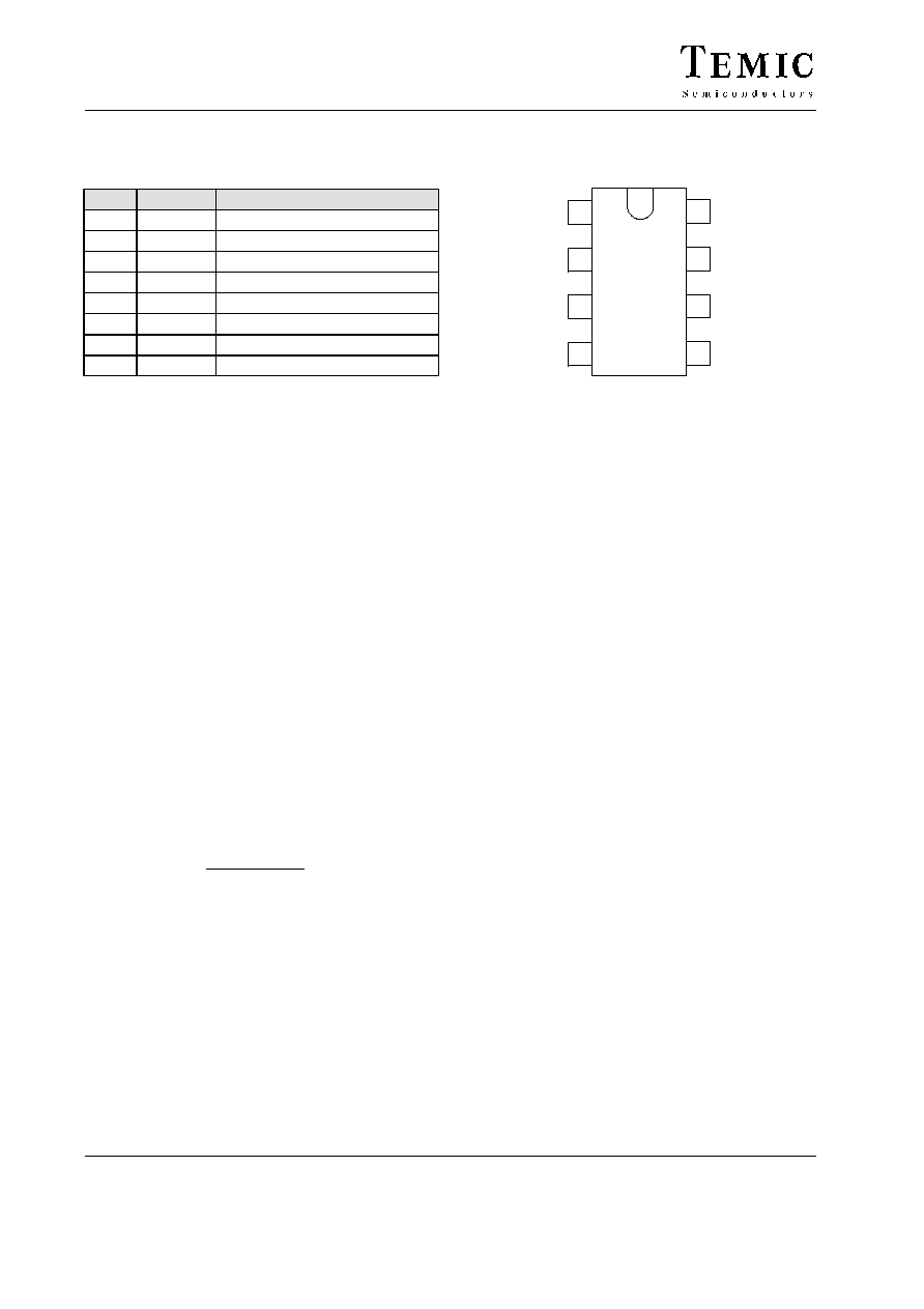
Ordering Information
Extended Type Number
Package
Remarks
U2043B
DIP8
U2043B≠FP
SO8
Block Diagram
V
6
≠81 mV
23 V
Pulse
generator
IC Ground
3.8 k
W
3.3 k
W
Relay
7
3
8
+ V
S
+ 49
R
3
100
W
R
1
49 a
4
5
K
1
K
3
C
1
R
1
6
2
13283
49 a≠Comparator
21 W
21 W 5 W
21 W
21 W
5 W
GND
≠ 31
R
2
Indicator lamps
Measuring comparator
Shunt
30 m
W
V
6
≠5 V
1
Pilot lamp
5 W
Pilot lamps
Figure 1.
U2043B
TELEFUNKEN Semiconductors
Rev. A2, 25-Feb-97
2 (6)
Pin Description
Pin
Symbol
Function
1
GND
IC ground
2
V
S
Supply voltage V
S
3
REL
Relay driver
4
OSC
C
1
oscillator
5
OSC
R
1
oscillator
6
V
S
Supply voltage V
S
7
LD
Lamp failure detection
8
SI
Start input (49a)
1
2
3
4
8
7
6
5
GND
Vs
REL
OSC
OSC
Vs
LD
12749
SI
U2043B
Figure 2. Pinning
Functional Description
Pin 1, GND
The integrated circuit is protected against damage via
resistor R
4
to ground (≠31) in the case of battery reversal.
An integrated protection circuit together with external
resistances R
2
and R
4
limits the current pulses in the IC.
Pin 2, Supply voltage, V
S
- Power
The arrangement of the supply connections to Pin 2 must
be such as ensure that, on the connection printed circuit
board (PCB), the resistance of V
S
to Pin 6 is lower than
that to Pin 2.
Pin 3, Relay control output (driver)
The relay control output is a high-side driver with a low
saturation voltage and capable to drive a typical automo-
tive relay with a minimum coil resistance of 60
W.
Pin 4 and 5 Oscillator
Flashing frequency, f
1
, is determined by the R
1
C
1
compo-
nents as follows (see figure 1):
f
1
[
1
R
1
C
1
1.5
Hz
where
C
1
47
mF
R
1
+ 6.8 kW to 510 kW
In the case of a lamp outage (see Pin 7) the oscillator
frequency is switched to the lamp outage frequency f
2
with f
2
[ 2.2 f
1
.
Duty cycle in normal flashing mode: 50%
Duty cycle in lamp outage mode: 40% (bright phase)
Pin 6, Supply voltage, Sense
For accurate monitoring via the shunt resistor, a mini-
mized layer resistance from point V
S
/ shunt to Pin 6 is
recommended.
Pin 7, Lamp outage detection
The lamp current is monitored via an external shunt
resistor R
3
and an internal comparator K1 with its
reference voltage of typ. 81 mV (V
S
=
12 V). The outage
of one lamp out of two lamps is detected according to the
following calculation:
Nominal current of 1 lamp: 21 W / (V
S
= 12 V):
I
lamp
= 1.75 A
Nominal current of 2 lamps: 2 x 21 W / (V
S
= 12 V):
I
lamp
= 3.5 A.
The detection threshold is recommended to be set in the
middle of the current range: I
outage
[ 2.7 A
Thus the shunt resistor is calculated as:
R
3
= V
T
(K1) / I
outage
R
3
= 81 mV/2.7 A = 30 m
W.
Comparator K1`s reference voltage is matched to the
characteristics of filament lamps (see "control signal
threshold" in the data part).
The combination of shunt resistor and resistance of wire
harness prevents Pin 7 from a too high voltage in the case
of shortet lamps.
Pin 8, Start input
Start condition for flashing: the voltage at Pin 8 has to be
below less than V
S
≠ 5 V (flasher switch closed).
Humidity and dirt may decrease the resistance between
49 a and GND. If this leakage resistance is
u 5 kW the IC
is still kept in its off-condition. In this case the voltage at
Pin 8 is greater than V
S
≠ 5 V.
During the bright phase the voltage at Pin 8 is above the
K2
threshold, during the dark phase it is below the K3
threshold. For proper start conditions a minimum lamp
wattage of 10 W is required.

U2043B
TELEFUNKEN Semiconductors
Rev. A2, 25-Feb-97
3 (6)
Absolute Maximum Ratings
Reference point Pin 1
Parameters
Symbol
Value
Unit
Supply voltage
Pins 2, 6
V
S
16.5
V
Surge forward current
t
p
= 0.1 ms
Pins 2, 6
t
p
= 2 ms
Pins 2, 6
t
p
= 2 ms
Pin 8
I
FSM
I
FSM
I
FSM
1.5
1.0
50
A
A
mA
Output current
Pin 3
I
O
0.3
A
Power dissipation
T
amb
= 95
∞
C
DIP8
SO8
P
tot
P
tot
420
340
mW
mW
T
amb
= 60
∞
C
DIP8
SO8
P
tot
P
tot
690
560
mW
mW
Junction temperature
T
j
150
∞
C
Ambient temperature range
T
amb
≠40 to +95
∞
C
Storage temperature range
T
stg
≠55 to +150
∞
C
Thermal Resistance
Parameters
Symbol
Value
Unit
Junction ambient
DIP8
SO8
R
thJA
R
thJA
110
160
K/W
K/W
Electrical Characteristics
Typical values under normal operation in application circuit figure 1, V
S
(+49, Pins 2 and 6) = 12 V.
Reference point ground (≠31), T
amb
= 25
∞
C, unless otherwise specified
Parameters
Test Conditions / Pins
Symbol
Min.
Typ.
Max.
Unit
Supply voltage range
Pins 2, 6
V
S
(+49)
9 to 15
V
Supply current
Dark phase or
stand-by
Pins 2, 6
I
S
4.5
8
mA
Supply current
Bright phase
Pins 2, 6
I
S
7.0
11
mA
Relay output
Saturation voltage
I
O
= 150 mA,
V
S
= 9 V
Pin 3
V
O
1.0
V
Relay output
reverse current
Pin 3
I
O
0.1
mA
Relay coil resistance
R
L
60
W
Start delay
First bright phase
t
on
10
ms
Frequency determining
resistor
R
1
6.8
510
k
W
Frequency determining
capacitor
C
1
47
mF

