
U2044B
TELEFUNKEN Semiconductors
Rev. A1, 25-Feb-97
1 (6)
Dual Output Flasher
Description
The integrated circuit U2044B is used in relay controlled
automotive flashers. With two output stages each side of
the vehicle is controlled separately. A left and a right
direction indicator input with only a small control current
makes switch contacts for small loads possible.
The separate hazard warning input simplifies the
construction of the hazard switch. Lamp outage is indi-
cated by frequency doubling during direction mode.
Thanks to the extreme low current consumption U2044B
can be connected to the battery directly.
Features
D Temperature and supply voltage compensated
flashing frequency
D Frequency doubling indicates lamp outage
D Two relay driver outputs with high current-carrying
capacity and low saturation voltage
D Minimum lamp load for flasher operation: w1 W
D Very low susceptibility to EMI
D Protection according to ISO/TR7637/1 level 4
D Extremly low current consumption < 10 mA
(@switches open)
D Reverse polarity protection
D Three control inputs: left, right and hazard warning
Ordering Information
Extended Type Number
Package
Remarks
U2044B
DIP14
U2044B-FP
SO14
Pin Description
Pin
Symbol
Function
1
OSC
Oscillator
2
SIL
Start input left
3
SIR
Start input right
4
SIHW
Start input hazard warning
5
V
S
V
S
6
CR1
Control input relay 1
7
CR2
Control input relay 2
8
LD
Lamp failure detection
9
V
S
V
S
10
GND
IC ground
11
OR1
Output relay 1
12
V
S
V
S
13
OR2
Output relay 2
14
OSC
Oscillator
1
2
3
4
14
13
12
11
OSC
SIR
SIHW
OSC
OR2
Vs
OR1
SIL
5
6
7
10
9
8
12750
V
S
CR1
CR2
GND
V
S
LD
U2044B
Figure 1. Pinning
U2044B
TELEFUNKEN Semiconductors
Rev. A1, 25-Feb-97
2 (6)
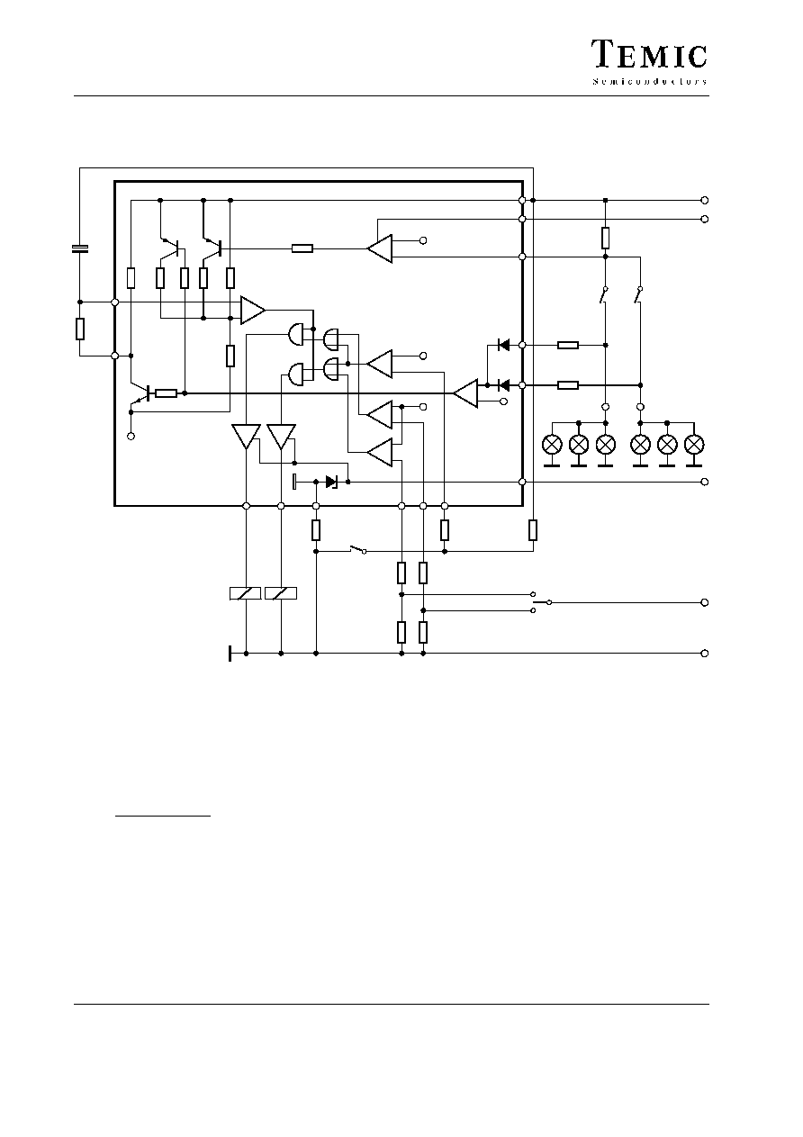
Block Diagram
+
�
+
�
+
�
�
+
�
+
27.5 V
+
�
V
Ref2
V
Ref1
V
S
�81 mV
6
7
8
5
9
GND 10
13
11
3
2
4
47 k
W
12
V
S
/2
R
9
47 k
W
R
8
R
Shunt
Contact
1
2
14
1
V
S
�6 V
4.7
mF
82 k
W
R
1
C
1
220
W
R
2
Hazard warning
4.7 k
W
R
3
4.7 k
W
R
6
R
4
1.2 k
W
R
10
right
left
1.2 k
W
R
7
1.2 k
W
R
5
1
2
Relay
30
30
30
15
31
12700
30 m
W
4.7 k
W
K1
Figure 2. Application circuit
R
2
for protection against continous reversed polarity: 1 Watt
Functional Description
Pin 1 and Pin 14, Oscillator
Flashing frequency, f
1
, is determined by the R
1
C
1
components as follows (see figure 2):
f
1
[
1
R
1
C
1
1.5
Hz
where
C
1
47
mF
R
1
+ 6.8 kW to 510 kW
In the case of a lamp outage the oscillator frequency is
switched to the lamp outage frequency f
2
with
f
2
[ 2.2 f
1
.
Duty cycle in normal flashing mode: 50%
Duty cycle in lamp outage mode (bright phase): 40%
Pin 2 and Pin 3, Start input right and left
Flashing is disabled as long as the input comparator is tied
zu GND (pull-down resistor R
7
or R
5
). The high side
flasher switch "left" or "right" changes the comparator
status and enables the output stage at Pin 11 or Pin 13. R
6
and R
4
are protection resistors for the input stage.
With an open flasher switch the current consumption is
only I
t 10 mA. The IC kept in stand-by mode until there
is a voltage drop of V
[ 6.9 V at the pull-down resistor.
Direction mode can only be activated when the ignition
switch is in ON-position as shown in figure 2.
Pin 4, Start input hazard warnig
In contrast to the direction switches, the hazard input is
U2044B
TELEFUNKEN Semiconductors
Rev. A1, 25-Feb-97
3 (6)
a low-side type. The pull-up resistor R
10
provides the off-
state. R
3
is a protection resistor for the input stage.
Hazard warning can be activated independent of the igni-
tion switch position.
Pin 5, Supply voltage sense
This pin supplies the lamp outage comparator at Pin 8 and
is externally connected to the battery (Kl 30).
Pin 6 and 7, Control input relay 1 and 2
The feedback detects the bright phase and the dark phase
and enables the oscillator.
Pin 8, Lamp outage detection
The lamp current is monitored via an external shunt
resistor, R
Shunt
and an internal comparator K1 with its
reference voltage of typ. 81 mV (V
S
=
12 V). The outage
of one lamp out of two lamps is detected according to the
following calculation:
Nominal current of 1 lamp: 21 W / (V
S
= 12 V):
I
lamp
= 1.75 A
Nominal current of 2 lamps: 2 x 21 W / (V
S
= 12 V):
I
lamp
= 3.5 A.
The detection threshold is recommended to be set in the
middle of the current range: I
outage
[ 2.7 A
Thus the shunt resistor is calculated as:
R
Shunt
= V
T
(K1) / I
outage
R
Shunt
= 81 mV/2.7 A = 30 m
W.
Comparator K1`s reference voltage is matched to the
characteristics of filament lamps (see "control signal
threshold" in the data part).
The combination of shunt resistor and resistance of wire
harness prevents Pin 8 from a too high voltage in the case
of shortet lamps.
Pin 9, Supply voltage
This pin supplies the oscillator, the comparators and the
logic parts of the IC.
Pin 10, GND
The integrated circuit is protected against transients
according to ISO�TR 7637�3 level 3 via resistor R
2
to
ground (�31). An integrated protection circuit together
with external resistors R
2,
R
3,
R
4,
R
6,
R
8
and R
9
limits the
current pulses in the IC. Against reversed battery the IC
is also protected .
Pin 11 and 13, Control output relay 1 and 2
The relay control outputs are high-side driver with a low
saturation voltage and capable to drive a typical
automotive relay with a coil resistance of 60
W.
Pin 12, Supply voltage power
This pin supplies the relay drivers connected directly to
the battery (Kl 30). It is internally clamped by a 27-V
Z-diode.
Absolute Maximum Ratings
Reference point ground (terminal 31), with external circuitry.
Parameters
Symbol
Value
Unit
Supply voltage, 1 min
Pins 5, 9, 12
V
S
24
V
Junction temperature
T
j
150
�
C
Storage temperature range
T
stg
�55 to +150
�
C
Ambient temperature range
T
amb
�40 to +100
�
C
Thermal Resistance
Parameters
Symbol
Value
Unit
Junction ambient
DIP14
SO14
R
thJA
R
thJA
90
120
K/W
K/W

U2044B
TELEFUNKEN Semiconductors
Rev. A1, 25-Feb-97
4 (6)
Electrical Characteristics
Typical values under normal operation in application circuit figure 1, V
S
(+30) = 12 V.
Reference point ground (�31), T
amb
= 25
�
C, unless otherwise specified.
Parameters
Test Conditions / Pins
Symbol
Min.
Typ.
Max.
Unit
Supply voltage range
Pins 5, 9, 12
V
S
8
18
V
Supply current,
switches open
Pins 5, 9, 12
I
S
10
mA
Output current for relay
driver
Pins 11, 13
I
O
300
mA
Saturation voltage
R
L
= 82
W Pins 11, 13
V
S
= 8 V
V
S
= 12 V
V
O
1.0
1.2
V
V
Relay coil resistance
R
L
60
W
Relay output,
reverse current
Pins 11, 13
I
O
0.1
mA
Start delay
(first bright phase)
t
ON
10
ms
Control signal threshold
V
S
= 9 V
Pin 8
V
S
= 13.5 V
V
S
= 16 V
V
S
70.6
85.0
93.0
mV
mV
mV
Tolerance of control signal
threshold
V
S
= 9 to 16 V,
Pin 8
T
amb
= �40 to +100
�
C
�6
+6
%
Temperature coefficient of
control signal threshold
V
S
= 13.5 V
Pin 8
T
K
10
mV/K
Clamping voltage
T
amb
= �40 to +100
�
C
V
12
25.0
27.5
30.0
V
Relay output overvoltage
detection (relay disabled)
T
amb
= �40 to +100
�
C
V
12
18
20
22
V
Tolerances
V
S
= 9 to 18 V, T
amb
= �40 to +100
�
C
Parameters
Test Conditions / Pins
Symbol
Min.
Typ.
Max.
Unit
Frequency determining
resistor
R
1
6.8
510
k
W
Frequency determining
capacitor
C
1
47
mF
Frequency tolerance
(normal flashing basic fre-
quency f
1
not including the
tolerance of the external
components R
1
and C
1
)
Df
1
�5
+5
%
Bright period (basic fre-
quency f
1
)
DF
1
47
53
%
Bright period
(control frequency f
2
)
Df
2
37
45
%
Frequency increase
(lamp failure)
f
2
2.15
f
1
2.3
f
1
Hz
Lamp load
P
L
1
W

U2044B
TELEFUNKEN Semiconductors
Rev. A1, 25-Feb-97
5 (6)
Package Information
13020
technical drawings
according to DIN
specifications
4.8 max
Package DIP14
Dimensions in mm
20.0 max
1.64
1.44
3.3
0.5 min
0.58
0.48
2.54
15.24
14
8
1
7
7.77
7.47
6.4 max
0.36 max
9.8
8.2
13035
technical drawings
according to DIN
specifications
Package SO14
Dimensions in mm
0.25
0.10
8.75
0.4
1.27
7.62
1.4
5.2
4.8
3.7
3.8
6.15
5.85
0.2
14
8
14
8