 | –≠–ª–µ–∫—Ç—Ä–æ–Ω–Ω—ã–π –∫–æ–º–ø–æ–Ω–µ–Ω—Ç: U2100B | –°–∫–∞—á–∞—Ç—å:  PDF PDF  ZIP ZIP |

U2100B
TELEFUNKEN Semiconductors
Rev. A1, 30-May-96
1 (9)
Timer Control for Triac and Relay
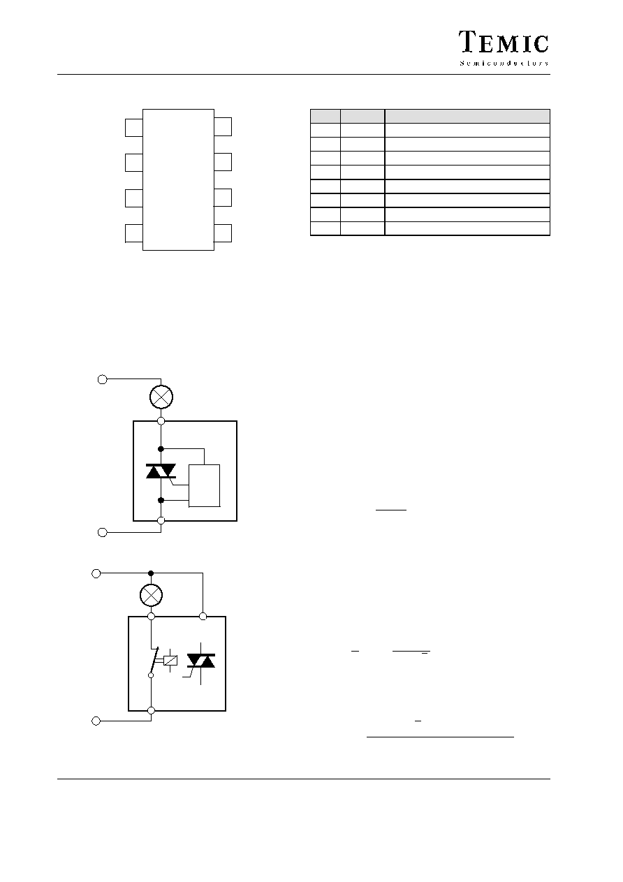
Description
The timer control circuit, U2100B, uses bipolar technol-
ogy. It has different mode selections (Zero voltage switch,
Phase control, Relay control). The output stage is
triggered according to input conditions. It can be used in
triac application for two or three wire system as a power
switch.
Features
D Adjustable and retriggerable tracking time
D Window monitoring for sensor input
D Enable input for triggering
D Internal noise suppression (40 ms) and retrigger
blocking (640 ms)
D Two or three wire application
Applications
D Motion detectors
D Touch sensors
D Timer
Package:
DIP8, SO8
V
mains
Supply voltage
limitation
Voltage control
monitoring
Noise
suppression
40 ms
Retrigger
delay
640 ms
Mode
Sync
Control
logic
Trigger
window
+
≠
+
≠
≠V
Ref
0.6 V
Ref
0.6 V
Ref
ON
0.5 V
Ref
OFF
RC Oscillator
Divider 1:2
10
7
0.5 V
Ref
En-
able
C
t
R
t
5
6
Trigger
signal
C
2
8
C
1
R
1
R
sync
D
1
2
≠V
S
4
R
G
3
1
Output
GND
L
N
Load
95 9876
selection
Z
Figure 1. Block diagram with external circuit
U2100B
TELEFUNKEN Semiconductors
Rev. A1, 30-May-96
2 (9)
Pin Description
1
2
3
4
8
7
6
5
95 9945
GND
≠V
S
Output
Sync
V
Ref
Osc
TRIG
EN
Pin
Symbol
Function
1
GND
Reference point
2
≠V
S
Supply voltage
3
Output
Driver output
4
Sync
Synchronisation and mode selection
5
EN
Enable
6
TRIG
Input trigger signal
7
Osc
RC Oscillator
8
V
Ref
Reference voltage
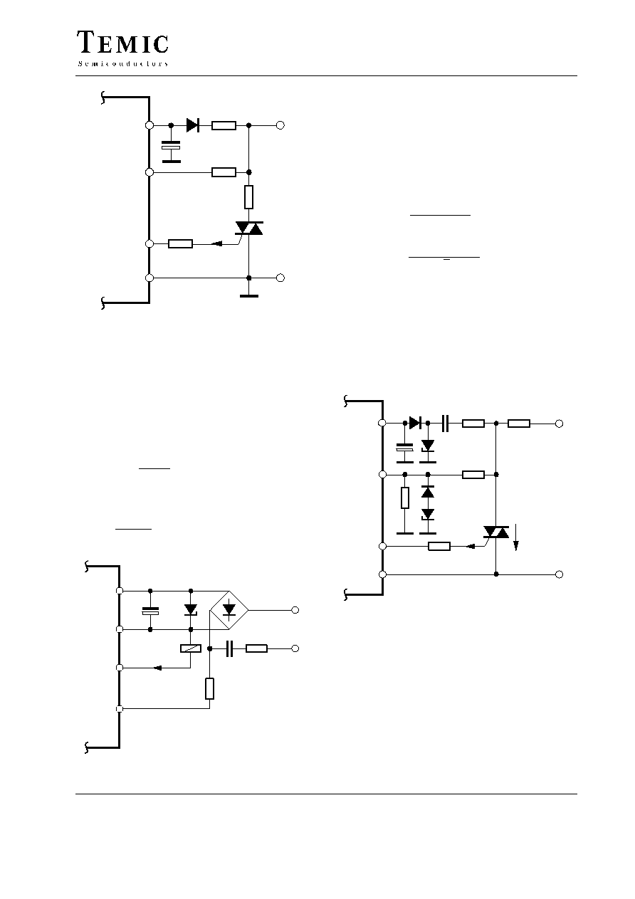
General Description
Monostable integrated power control circuit, U2100B,
can be used according to mode selection in relay's or
triac's applications. Beyond that, it can be used in triac-
application for two wire system as power switch, (being
the load in series to the switch) whereas the supply
voltage for the control unit is gained from phase rest angle
(
a
min
-operation).
Control
L
N
95 9949
Figure 2. Two wire circuit
Control
L
N
95 9950
Figure 3. Three wire circuit
For three wire switch, two modes of operations are
possible:
≠
Zero voltage switch operation for triac control
≠
Static operation for relay control
Mode Selection Pin 4 and Supply Voltage
Pin 2
Operation modes can be selected by external voltage at
the sync. input Pin 4 (clamping). Mode selection deter-
mines the current requirement of driver stage for relay's
or triac's and hence the selection of supply voltage.
Zero Voltage Switch Operation, Figure 4
Selection condition:
V
4
= internal sync limitation, without external clamping
R
1
[ 0.85
V
M
≠V
S
2 I
tot
I
tot
= I
S
+ I
p
+ I
X
whereas:
I
S
= Supply current of IC without load
I
P
= Average trigger current I
G
I
X
= External circuit current requirement
V
M
= Mains voltage
Required firing pulse width t
p
t
p
+ 2w arcsin
I
L
V
M
P
2
whereas:
I
L
= Triac latching current
P
= Power at load Z
R
sync
[k
W] [
V
M
[V]
2 sin w t
p
[s] ≠ 0.7
1.8
10
≠2
≠176
U2100B
TELEFUNKEN Semiconductors
Rev. A1, 30-May-96
3 (9)
2
≠V
S
4
Sync
R
sync
R
G
3
Output
C
1
D
1
R
1
I
G
Z
1
L
N
V
M
95 9951
GND
Figure 4.
DC Operation, Figure 5
Selection condition:
+V
4
= 6.1 V ≠V
4
= int. limitation
whereas:
R
0
[ 1 10 X
c
X
c
+ 0.85
V
M
≠V
S
I
tot
I
tot
+ I
S
) I
Rel
) I
X
C
0
+
1
w X
C
2
≠V
S
R
sync
3
Output
C
1
I
Rel
1
GND
95 9952
BZX85C22V
4
Sync
C
o
R
o
Rel
N
L
V
M
230 V~
4xBYX86
Figure 5.
a
min
-operation, Figure 6
Selection condition:
≠V
4
= 6.5 to 7.8 V
+V
4
= int. limitation
R
amax
+ R
sync
3.6 V
V
R(peak)
≠3.6 V
R
amin
+ R
sync
10 V
V
M
2 ≠10 V
V
R(peak)
is the peak voltage of the rest phase angle, which
should be high enough to generate the supply voltage, V
S
.
I
G
V
R(peak)
BZX85
C22V
N
V
M
230 V~
2
≠V
S
4
Sync
R
sync
R
G
3
Output
C
1
Z
1
GND
L
95 9953
C
o
R
o
1N4148
BZX55
6V8
R
a
D
1
IN 4007
Figure 6.
C
1
=
100
mF/35 V
C
o
=
0.33
mF/250 V
R
o
=
390
W
R
sync
=
220 k
W
R
a
=
10 k
W
R
G
=
390
W
D
1
=
IN 4007

U2100B
TELEFUNKEN Semiconductors
Rev. A1, 30-May-96
4 (9)
Tracking Time Pin 7
An internal RC oscillator with following divider stage
1:2
10
allows a very long and reproducible tracking time.
RC-values for required final time, t
t
, can be calculated as
follows:
R
t
[
W] +
t
t
[s] 10
6
1.6 1024 C
t
[
mF]
C
t
[
mF] +
t
t
[s] 10
6
1.6 1024 R
t
[
W]
t
t
[s]
+
C
t
[
mF] R
t
[
W] 1.6 1024
10
6
Trigger Inputs Pins 5 and 6, Figures 7 and 8
Two AND-connected, identical inputs determine the
trigger conditions of monostable time stages, i.e., both
inputs must be in position "ON" so that the output is
switched ON. The tracking time starts after the trigger
conditions has elapsed. The output ON state is given until
the tracking time is over.
Input Pin 5 is a simple comparator whereas input Pin 6 is
built up as a window discriminator.
Noise suppression for t
ON
= 40 ms guarantee, that there
is no peak noise signals at the inputs which could trigger
the circuit.
At the same time, the retrigger is delayed for a duration
of 640 ms (t
OFF
), to avoid noise signal to trigger the relay.
0
Hysteresis
95 9954
OFF
ON
T
1
= 0.5 V
Ref
T
2
= 0.6 V
Ref
V
Ref
V
5
Figure 7. Trigger condition, Pin 5
0
95 995
ON
T
1
+ 0.5 V
Ref
T
2
+ 0.65 V
Ref
V
Ref
V
6
ON
OFF
Figure 8. Trigger condition, Pin 6
U2100B
TELEFUNKEN Semiconductors
Rev. A1, 30-May-96
5 (9)
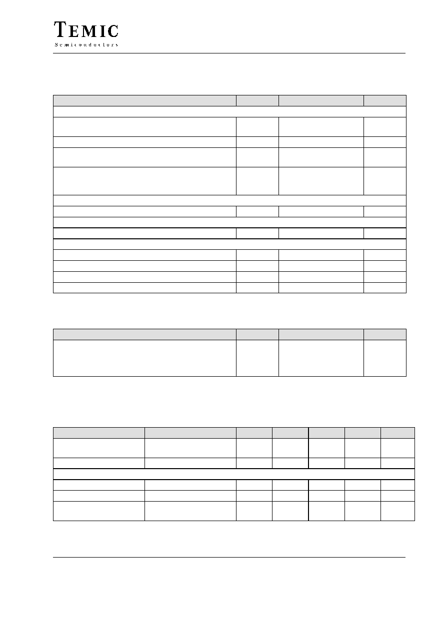
Absolute Maximum Ratings
Reference point Pin 1, unless otherwise specified
Parameters
Symbol
Value
Unit
Supply
Pin 2
Supply current
Peak current
t
10
ms
≠I
S
≠i
s
10
60
mA
Supply voltage
≠V
S
32
V
Reference voltage source
Pin 8
Output current
I
O
3
mA
Synchronization
Pin 4
Input current
t
10
ms
±
I
Sync.
i
Sync.
5
20
mA
Window monitoring
Input voltage
Pin 6
≠V
1
V
Ref
to 0
V
Enable-Schmitt trigger
Pin 5
Input voltage
≠V
1
V
Ref
to 0
V
Driver output
Pin 3
Collector voltage
≠V
o
V
S
to 2
V
Storage temperature range
T
stg
≠40 to +125
∞
C
Junction temperature
T
j
125
∞
C
Ambient temperature range
T
amb
0 to 100
∞
C
Thermal Resistance
Parameters
Symbol
Value
Unit
Junction ambient
DIP8
SO8 on PC board
SO8 on ceramic
R
thJA
110
220
140
K/W
Electrical Characteristics
V
S
= ≠18 V, T
amb
= 25
∞
C, reference point Pin 1, unless otherwise specified
Parameters
Test Conditions / Pins
Symbol
Min
Typ
Max
Unit
Supply voltage limitation
I
S
= 800
mA
Pin 2
I
S
= 2 mA
≠V
S
21
21.3
23
24
V
Current consumption
I
3
= 0
≠I
S
750
mA
Supply voltage monitoring
Pin 2
ON-Threshold
≠V
S
15
V
OFF-Threshold
≠V
S
6.5
V
Reference voltage
I
8
= 0.1 mA
Pin 8
I
8
= 1.5 mA
≠V
Ref
4.75
4.55
5.25
5.25
V