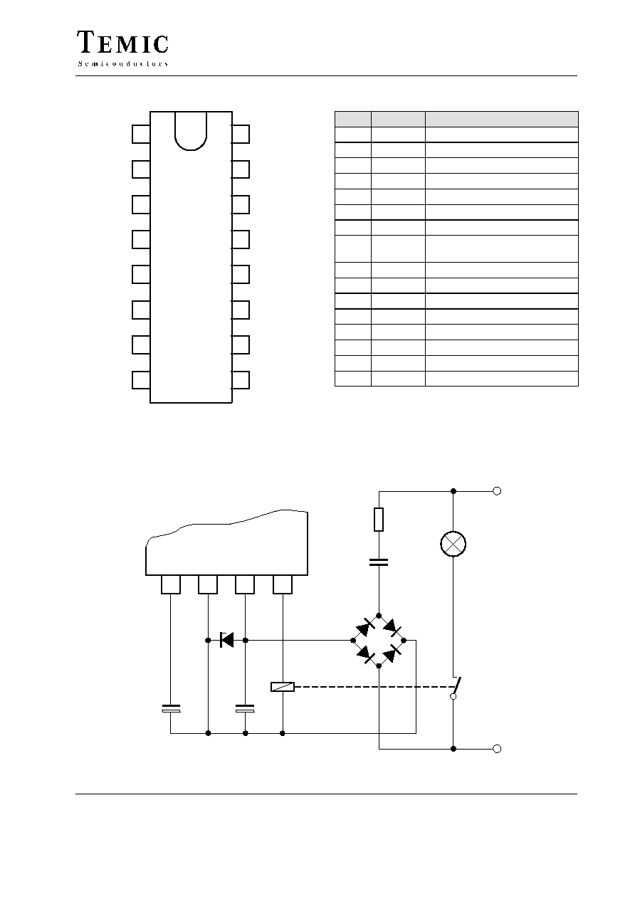
U2101B
TELEFUNKEN Semiconductors
Rev. A1, 30-May-96
1 (9)
Relay Timer
Description
The U2101B monolithic integrated bipolar circuit is a
versatile timer device for relay control. Because of two
integrated, freely configurable operational amplifiers, it
covers a very wide range of applications.
Features
D Adjustable window for trigger input
D Enable input for triggering
D Adjustable noise suppression
D Adjustable and retriggerable tracking time
D Enable and block delay
D Two integrated operational amplifiers *
freely connectable
D 50 mA relay driver
Applications
D Motion detectors
D Tracking controllers
D Multiple timer
D Conditional switches
D Clock generators
Package: DIP16, SO16
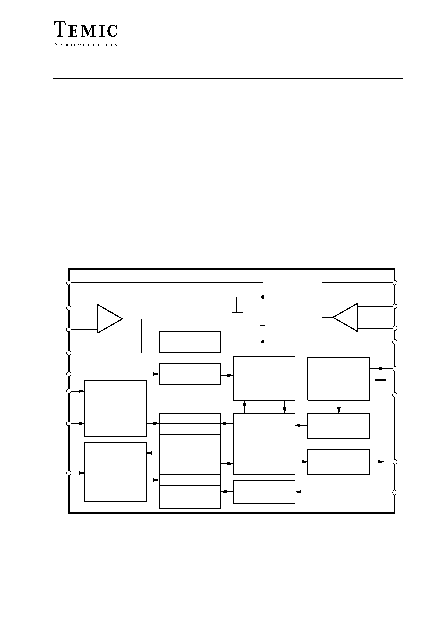
4
95 9738
V
Ref
≠ 5 V
Control logic
Noise
suppression
Timer 2, 3, 4
On: 4 T
osc2
Restart on: 64 T
osc2
On / Off: 1024 T
osc2
RC oscillator 2
Voltage
monitoring
Relay driver
50 mA
Voltage
limitation
Enable
schmitt trigger
Out (On): 0.1 V
Ref
Out (Off): 0.5 V
Ref
On: 0.6 V
Ref
Window adjustment
Trigger
window
Timer 1
1024 T
osc1
RC oscillator 1
+
≠
OP 1
+
≠
OP 2
5
6
GND
≠V
S
3
2
16
R
b
40 k
W
R
a
60 k
W
7
f
osc2
8
1
15
14
13
f
osc1
12
11
10
9
Figure 1. Block diagram

U2101B
TELEFUNKEN Semiconductors
Rev. A1, 30-May-96
4 (9)
Capacitor C
1
is calculated as follows:
X
C1
+ 0.85
V
mains
≠V
S
I
tot
where
I
tot
= I
S
+ I
Rel
+ I
X
I
S
= current consumption of the IC without load
I
Rel
= relay current
I
X
= current consumption of the external components
C
1
+
1
w X
C1
The following applies for R
1
:
R
1
[ 1
10
X
C1
At Pin 4, the circuit provides a stabilized reference
voltage of ≠5 V.
Voltage Monitoring
While the operating voltage is being built up or reduced,
uncontrolled states and activation of the output stage are
prevented by the internal monitoring circuit. All latches
in the circuit, the divider and the control logic are reset.
After the supply voltage is applied, a single operating
cycle is started independently of the trigger inputs in
order to immediately make the entire function visible.
Trigger Inputs, Pins 9 and 10
The trigger condition for the time stage is determined by
the two input Pins 9 and 10. To initiate a triggering opera-
tion, both inputs must be in the ON state, since they are
equivalent and AND connected. The tracking time begins
when the trigger condition finishes. The output remains
in the ON state until the tracking time is over.
The enable input, Pin 9, is designed as a comparator with
hysteresis. The blocking threshold is switched over by the
noise suppression in order to avoid faults as a result of
load switching (see figure 4).
The trigger input, Pin 10, is designed as a window dis-
criminator. The window is adjusted at Pin 11. When
V
11
= V
4
, the minimum window of approximately
250 mV is set. When V
11
= V
5
, the maximum window is
approximately 1 V. The window discriminator is in the
OFF state when the voltage at Pin 10 is within the window
set at Pin 11 (see figure 5).
If a resistor divider with a NTC resistor is connected at
Pin 11, it is possible to compensate for the temperature
dependence of an IR sensor, for example. This means that
the range becomes temperature independent.
0.6
V
Ref
V
Ref
0
V
9
0.5/0.1
V
Ref
Hysteresis
94 9299
OFF
ON
Figure 4. Trigger condition, Pin 9
0.05
V
Ref
+ 0.15
V
11≠4
OFF
0.6
V
Ref
V
Ref
0
V
10
95 9739
ON
ON
0.05
V
Ref
+ 0.15
V
11≠4
Figure 5. Trigger condition, Pin 10
Noise Suppression, Pin 8
The internal noise suppression ensures that peak noise
signals at the inputs do not cause undesired triggering.
Also, triggering is prevented for a certain time after the
load is switched off in order to avoid any intrinsic fault.
The delay times are derived from oscillator 2 at Pin 8, the
frequency, f
osc2
, of which is calculated as follows:
f
osc2
+
1
1.6 R
osc2
C
osc2
,
whereas
C
osc2
should not be greater than 1
mF.
This gives the period duration T
osc2
:
T
osc2
[s]
+ 1600 R
osc2
[k
W] C
osc2
[
mF]
The enable input, Pin 9, is buffered for 1024
T
osc2
during switching on and switching off, and the input of the
window discriminator at Pin 10 is buffered for 4
T
osc2
during switching on and for 64
T
osc2
in the case of
switching back on. Appropriately selecting R
osc2
and
C
osc2
at Pin 8 allows any delay times to be adjusted so that
they can be adapted to the respective requirements.

U2101B
TELEFUNKEN Semiconductors
Rev. A1, 30-May-96
5 (9)
RC Oscillator 1, Pin 12
The oscillator 1 with the following divider stage 1:1024
allows a very long and reproducible tracking time t
t
. The
circuitry of Pin 12 for a certain tracking time t
t
can be
calculated as follows:
R
osc1
[k
W] +
t
t
[s]
10
3
1.6
1024 C
osc1
[
mF]
whereas C
osc1
should not be greater than 1
mF.
Voltage Divider, Pin 1
Two freely connectable operational amplifiers, OP1 and
OP2, are used to evaluate several sensor signals. The tap
of a voltage divider between GND and V
Ref
with a voltage
level of 0.6
V
Ref
is available at Pin 1. The middle of the
discriminator window is also at this value. Assuming that
the output of one operational amplifier is connected at the
trigger input, Pin 10 (window discriminator), the dc
operating point of this operational amplifier can
be
adjusted without additional external resistors by
connecting the input to Pin 1. This value is approximately
in the center of the dynamic range of the OP.
Absolute Maximum Ratings
Reference point Pin 5, unless otherwise specified
Parameters
Symbol
Value
Unit
Power supply
Current
Pin 6
t < 10
ms
Pin 6
≠I
S
≠i
S
15
60
mA
mA
Reference voltage source
Output current
Pin 4
I
O
5
mA
Output stage
Output voltage
Pin 7
≠V
O
V
S
to 1.8
V
Input currents
Pin 13 and 16
"I
I
5
mA
Input voltages
Pins 1, 2, 3, 8, 9, 10, 11, 12, 14, 15
V
I
V
Ref
to 0
V
Storage temperature range
T
stg
≠40 to +125
∞
C
Junction temperature
T
j
+125
∞
C
Ambient temperature range
T
amb
≠10 to +100
∞
C
Thermal Resistance
Parameters
Symbol
Maximum
Unit
Junction ambient
DIP 16
SO 16 on PC board
SO 16 on ceramic
R
thJA
120
180
100
K/W