 | –≠–ª–µ–∫—Ç—Ä–æ–Ω–Ω—ã–π –∫–æ–º–ø–æ–Ω–µ–Ω—Ç: U2102B | –°–∫–∞—á–∞—Ç—å:  PDF PDF  ZIP ZIP |

U2102B
TELEFUNKEN Semiconductors
Rev. A1, 30-May-96
1 (16)
Multifunction Timer
Description
The monolithic integrated bipolar circuit U2102B is an
MOSFET or IGBT control circuit which allows
realization of an extremely wide range of timer and
dimmer functions. The integrated current monitoring
function additionally permits the power switch to be
reliably protected without an additional fuse.
Features
D Integrated reverse phase control
D Two- or three-wire applications
D Mode selection:
≠
Zero-voltage switch with static output
≠
Two-stage reverse phase control with switch-off
≠
Two-stage reverse phase control
D Current monitoring:
≠
High-speed short-circuit monitoring with output
≠
High-current monitoring with integrating buffer
D Integrated chip temperature monitoring
D Adjustable and retriggerable tracking time
D External window adjustment for sensor input
D Enable input for triggering
Applications
D Motion detectors
D Time-delay relays
D Dimmers
D Reverse phase controls
D Timers
Package: DIP16, SO16
V
Ref
Divider
Control
logic
Voltage limitation
Synchronization
Push
pull
RC oscillator
Triggering with buffers
Voltage monitoring
Temperature
monitoring
Reverse
phase
control
Programing
Current monitoring
Test logic
94 8666
16
14
9
6
7
12
8
5
1
15
10
2
13
11
4
3
Figure 1. Block diagram

U2102B
TELEFUNKEN Semiconductors
Rev. A1, 30-May-96
2 (16)
POR
33 k / 2
W
Ref
adjustment
V
oltage
Synchronization
Buf
fer
Current monitoring
Push pull
Load
V
W
indow
limitation
NTC
120 ms
68 k
R
1 nF
1 k
100
mains
230 V
47 F/25
V
IGBT
V
R
m
W
W
W
W
1 k
Stat. ZVS
Control
2
Ramp
7
820 k
C
10 nF
94 8220 e
W
RC oscillator
3
8
2 stage / out
6
1
V
5
220 nF
22 k
1 F
+ V
100k
C
4
1 M
R
Clock
GND
V
oltage
monitoring
Phase
Ref
Reverse
S
Control
Divider
(spike-
+
Buf
fer
T
est mode
Clock
Enable
Clock
logic
filter)
signal
T
rigger
W
W
W
m
V
Ref
+
≠
≠
T
rigger window
Enable
+
≠
GND
+ V
S
V
Ref
2 stage
W
Clock
generator
T
est logic
10
16
9
100 mV
500 mV
14
+
11
12
13
15
+
≠
≠
Q
R
Q
T
emp
S
monitoring
X
+Vs
GND
Control
0.02xV
0.1/0.4/
0.5 x
V
2
3
R
3
C
2
Ref
0.55 x
V
+ 0.2
V
Ref
9
0.45 x
V
≠ 0.2 x
V
Ref
9
1
C
1
R
G
sh
Ref
Ref
Figure 2. Block diagram with typical circuit for dc loads

U2102B
TELEFUNKEN Semiconductors
Rev. A1, 30-May-96
3 (16)
Pin Description
Pin
Symbol
Function
1
V
Ref
Reference voltage 5 V
2
C
Ramp
Ramp, capacitance
3
R
Ramp
Current setting for ramp
4
Control
Control voltage
5
Osc
RC oscillator
6
Prog.
Tri state programing
7
EN
Enable-input
8
Trigger
Trigger-input (window)
9
V
9
Window-adjustment
10
Test
Test output
11
I
I
Input current monitoring
12
I
off
Fast output current monitoring
13
GND
Ground
14
V
O
Output voltage
15
+ V
S
Supply voltage
16
Sync
Synchronization input
1
2
3
4
5
6
7
8
16
15
14
13
12
11
10
9
V
Ref
C
Ramp
R
Ramp
Control
Osc
Prog.
EN
Trigger
Sync
+V
S
V
O
GND
I
off
I
I
Test
V
9
94 8619

U2102B
TELEFUNKEN Semiconductors
Rev. A1, 30-May-96
4 (16)
Power Supply, Synchronization Pins 15 and 16
The voltage limitation circuit contained in the U2102B
enables simple power supply via a dropping resistor R
1
.
In the case of dc loads, practically all the supply current
flows into Pin 16 (the pull down resistor at Pin 16 is neces-
sary in order to guarantee reliable synchronization) and
is supplied via an internal diode to Pin 15, where the resul-
tant supply voltage is limited and smoothed by C
1
. As a
result, the rectified and divided line voltage appears at
Pin 16, where the amplitude is limited. The power supply
for the circuit can be realized in all modes for dc loads as
shown in figure 3. The voltage at Pin 16 is used to
synchronize the circuit with the mains and generate the
system clock required for the buffers. The circuit detects
a "zero crossing" when the voltage at Pin 16 falls below
an internal threshold of approximately 8 V.
Voltage
limitation
Push
pull
Sync.
16
15
14
13
GND
+V
S
R
1
=R
sync
R
G
V
mains
Load
IGBT
R
sh
C
1
95 9882
Temp.
monit.
Figure 3. Power supply for dc loads (R
1
is identical with R
sync
)
R
1
is calculated here as follows:
R
1max
+ 0.85
V
Nmin
≠V
S
I
tot
(1)
where:
V
Nmin
=
V
mains
≠ 15%
V
S
=
Supply voltage
I
tot
=
I
Smax
+ I
x
I
Smax =
Max. current consumption of the IC
I
x
=
Current consumption of the external
components
U2102B
TELEFUNKEN Semiconductors
Rev. A1, 30-May-96
5 (16)
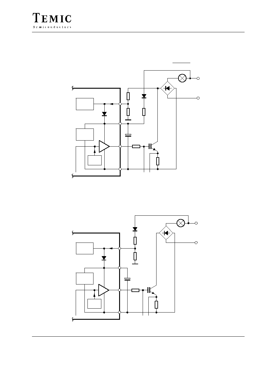
In the case of ac loads, it is necessary to make a distinction
for power supply purposes between the individual
operating modes. In reverse phase control mode, figure 4,
Pin 15 must be additionally supplied with power via a
dropping resistor, since no current flows in Pin 16 when
the power switch is switched on. Here, the dropping
resistor, R
1
, is connected before the rectifier bridge and
therefore has only one mains half-wave. R
1
is then calcu-
lated as follows:
R
1max
+ 0.85 @
V
Nmin
≠V
S
2
@ I
tot
Voltage
limitation
Temp.
monit.
Push
pull
Sync.
16
15
14
13
GND
+V
S
R
sync
R
G
Load
IGBT
R
sh
C
1
95 9883
D
1
R
1
V
mains
Figure 4.
Power supply in reverse phase
control mode for ac loads
In two-wire systems, the additional power supply at
Pin 15 is not possible (see figure 4, by omitting R
1
and
Diode D
1
). In this case, the resistor R
sync
is identical with
R
1
and should be as low as the power dissipation allows
it. A sufficiently large residual phase angle must remain
in this case in order to guarantee the device supply.
The power supply is simplified if the device is operated
as a static zero-voltage switch for ac loads (see figure 5).
All delay times are twice as long here, since synchro-
nization of the module is tapped before the rectifier
bridge.
Voltage
limitation
Temp.
monit.
Push
pull
Sync.
16
15
14
13
GND
+V
S
R
G
Load
IGBT
R
sh
C
1
95 9884
R
1
= R
sync
V
mains
Figure 5.
Power supply as static zero
voltage switch for ac loads