 | –≠–ª–µ–∫—Ç—Ä–æ–Ω–Ω—ã–π –∫–æ–º–ø–æ–Ω–µ–Ω—Ç: U2203B-A | –°–∫–∞—á–∞—Ç—å:  PDF PDF  ZIP ZIP |

U2203B
TELEFUNKEN Semiconductors
Rev. A2, 27-Jan-97
1 (7)
RGB Video Amplifier System for Monitors
Description
The U2203B-A is a wideband video amplifier IC system
especially designed for use in high-resolution RGB moni-
tors. The IC includes three well matched video
amplifiers, three gated differential amplifiers for black-
level clamping and brightness control and the function for
simultaneously contrast control. Separate adjustment of
the maximum gain of each channel is also possible.
Features
D 3 channels, high bandwidth (90 MHz @ ≠3 dB)
D Matched attenuators for contrast control
D Black-level clamping for brightness control
D Independent gain control of each amplifier
D ESD protection according to MIL-STD. 883
28 Vs1
1
Vs1
CONTRAST CAP
CONTRAST CAP
2
3
SUPPLY
REG.
1k
RED
40
26 R CLAMP (≠)
27 R DRIVE
24 R CLAMP (+)
25 R VIDEO OUT
90
4
5
R VIDEO IN
R CLAMP CAP
G VIDEO IN
GROUND
G CLAMP CAP
6
7
8
1k
GREEN
21 G CLAMP (≠)
22 G DRIVE
23 Vs2
19 G CLAMP (+)
20 G VIDEO OUT
40
1k
BLUE
9
10
B VIDEO IN
B CLAMP CAP
Vin REF
CONTRAST
11
12
CONTRAST
CONTROL
17 B CLAMP (≠)
18 B DRIVE
15 B CLAMP (+)
16 B VIDEO OUT
U2203B
13
14
Vs1
CLAMP GATE
1.4V
REF
2.4V
REF
95 10749
90
40
90
Figure 1. Block diagram
U2203B
TELEFUNKEN Semiconductors
Rev. A2, 27-Jan-97
2 (7)
Pin Description
1
2
3
4
5
6
7
8
10
9
27
22
21
20
18
19
17
12
11
28
25
26
23
24
V
in, G
GND
C
clamp, G
V
in, B
C
clamp, B
V
Bias
V
in, R
C
clamp, R
V
contr
C
contr
C
contr
V
S1
V
S2
R
G
V
G≠
V
out, G
V
G+
R
B
V
out, R
V
R+
V
B≠
V
R≠
R
R
V
S1
16
15
14
13
96 12388
V
S1
V
Gate
V
out, B
V
B+
Figure 2. Pinning
Pin
Symbol
Function
1
V
S1
Supply voltage
2
C
contr
Contrast cap.
3
C
contr
Contrast cap.
4
V
in, R
Video input (R)
5
C
clamp, R
Clamp cap. (R)
6
V
in, G
Video input (G)
7
GND
Ground
8
C
clamp, G
Clamp cap. (G)
9
V
in, G
Video input (B)
10
C
clamp, B
Clamp cap. (B)
11
V
Bias
Bias voltage (RGB-inputs)
12
V
contr
Contrast control
13
V
S1
Supply voltage
14
V
Gate
Inverted clamp gate
15
V
B+
Clamp amplifier (B+)
16
V
in, B
Video output (B)
17
V
B≠
Clamp amplifier (B≠)
18
R
B
Drive resistor (B)
19
V
G+
Clamp amplifier (G+)
20
V
out, G
Video output (G)
21
V
G≠
Clamp amplifier (G≠)
22
R
G
Drive resistor (G)
23
V
S2
Supply voltage (outputs)
24
V
R+
Clamp amplifier (R+)
25
V
out, R
Video output (R)
26
V
R≠
Clamp amplifier (R≠)
27
R
R
Drive resistor (R)
28
V
S1
Supply voltage
Absolute Maximum Ratings
Parameters
Symbol
Value
Unit
Supply voltage
Pins 1, 13, 28 and 23
V
S
13.5
V
Input voltage at all other pins
V
in
0 toV
S
V
Video output current
Pins 16, 20 and 25
I
V
28
mA
Junction temperature
T
j
125
∞
C
Storage temperature range
T
stg
≠40 to 125
∞
C
Operating Range
Parameters
Symbol
Value
Unit
Ambient temperature range
T
amb
0 to 80
∞
C
Supply voltage range
Pins 1, 13, 23 and 28
V
S2
, V
S1
11.0 to 13.0
V
U2203B
TELEFUNKEN Semiconductors
Rev. A2, 27-Jan-97
3 (7)
Thermal Resistance
Parameters
Symbol
Value
Unit
Junction ambient
(DIP28)
R
thJA
46
K/W
Electrical Characteristics
Test conditions unless otherwise specified, reference point Pin 7, T
amb
= 25
∞
C,
V
S1
= V
S2
= 12 V, V
12
= 6 V (contrast); V
14
= 0 V (inv. gating); V
15
= V
19
= V
24
= 2 V (brightness)
Parameters
Test Conditions / Pins
Symbol
Min.
Typ.
Max.
Unit
DC-values
Supply current
V
S1
only,
Pins 1, 13 and 28
I
S1
60
70
mA
Input bias voltage
Pin 11
V
inREF
2.3
2.5
V
Input bias current
Pins 4, 6 and 9
I
inREF
1
5
10
mA
Switching voltage gating
"on"
Pin 14
VG "L"
0.8
1.3
V
Switching voltage gating
"off"
Pin 14
VG "H"
1.5
2.0
V
Switching current gating
"on"
V
14
= 0.8 V
Pin 14
IG "L"
≠1
≠0.01
mA
Switching current gating
"off"
V
14
= 2.0 V
Pin 14
IG "H"
5
8
mA
Charge current clamping
capacitor
V
5,8,10
= 0 V
Pins 5, 8 and 10
ICL+
0.8
1.0
1.2
mA
Discharge current clamping
capacitor
V
5,8,10
= 5 V
Pins 5, 8 and 10
ICL≠
≠1.2
≠1.0
≠0.8
mA
Video outputs, V
O
Pins 16, 20 and 25
Low level
V
5,8,10
= 0 V
V
O"L"
0.8
1.0
V
High level
V
5,8,10
= V
S
V
O"H"
8.0
8.6
V
Output offset between two
amplifiers
V
15
, V
19
, V
24
= 2 V
DV
O
(2 V)
±
50
mV
p
V
15
, V
19
, V
24
= 4 V
DV
O
(4 V)
±
50
mV
Video gain
V
15
= V
19
= V
24
= 4 V (brightness); f
IN
= 1 MHz
Maximum video gain
V
12
= 12 V
G
Vmax
16.0
17.7
dB
Middle video gain
V
12
= 5 V
GV
mid
8.5
dB
Dynamic gain range
GVD
50
dB
Video gain match
(any 2 outputs)
V
12
= 12 V
V
12
= 5 V
V
12
= 2.2 V 1)
GVM
max
GVM
mid
GVM
≠30
±
0.1
±
0.1
±
0.3
dB
dB
dB
Video bandwidth
unpeaked (C = 0 pF)
optimal peaking
(C = 27 pF)
V
12
= 12 V (f
≠3dB
)
V
12
= 12 V (f
≠3dB
)
BWV
BWV
P
65
90
MHz
MHz
Video cross talk
f
IN
= 10 kHz
f
IN
= 10 MHz
CT
10kHz
CT
10MHz
≠50
≠47
dB
dB
1)
Measured 30 dB below maximum gain
U2203B
TELEFUNKEN Semiconductors
Rev. A2, 27-Jan-97
4 (7)
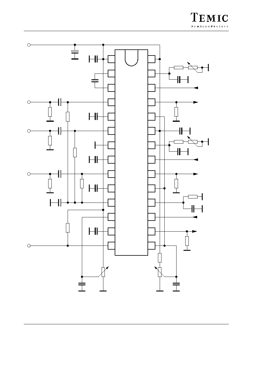
28
27
26
25
1
2
3
4
U2203B
24
23
22
5
6
7
21
8
9
10
11
12
13
14
20
19
18
17
16
15
100 nF
100 nF
100 nF
100 nF
100 nF
100 nF
10 k
W
10 k
W
10 k
W
100
mF
5
mF
75
W
R Video in
5
mF
75
W
75
W
5
mF
5
mF
10 k
W
V
S
(+12V)
G Video in
B Video in
51
W
100
W
C
R Clamp (≠)
390
W
To cascade
driver (R)
51
W
100
W
C
G Clamp (≠)
390
W
To cascade
driver (G)
91
W
C
390
W
To cascade
driver (B)
10 k
W
Black level
(brightness)
control
Black level
gate I/P
10 k
W
10 nF
Contrast
control
0 ... 12 V
100 nF
10 k
W
93 7632
100 nF
G Clamp (≠)
Figure 3. Typical application circuit

U2203B
TELEFUNKEN Semiconductors
Rev. A2, 27-Jan-97
5 (7)
AC Characteristics
0
2
4
6
8
10
12
14
16
18
20
1
10
100
1000
Gain ( dB )
Frequency ( MHz )
95 10748
C = 0 pF
C = 10 pF
C = 27 pF
C = 47 pF
Figure 4. Gain vs. frequency (various peaking), V
12
= 12 V (contrast), V
15
= V
19
= V
24
= 4 V (brightness)
≠60
≠50
≠40
≠30
≠20
≠10
0
10
1
10
100
1000
Relative gain ( dB )
Frequency ( MHz )
95 10747
Figure 5. Relative gain vs. frequency (no peaking), V
12
= variable (contrast), V
15
= V
19
= V
24
= 4 V (brightness),
0 dBrel = 17.7 dB, C = 0 pF