 | –≠–ª–µ–∫—Ç—Ä–æ–Ω–Ω—ã–π –∫–æ–º–ø–æ–Ω–µ–Ω—Ç: U2270B | –°–∫–∞—á–∞—Ç—å:  PDF PDF  ZIP ZIP |

U2270B
TELEFUNKEN Semiconductors
Rev. A3, 13-Dec-96
1 (13)
Read / Write Base Station IC
Description
IC for IDIC
Æ
*)
read-write base stations
The U2270B is a bipolar integrated circuit for read-write
base stations in contactless identification and immo-
bilizer systems.
The IC incorporates the energy transfer circuit to supply
the transponder. It consists of an on-chip power supply, an
oscillator, and a coil driver optimized for automotive-
specific distances. It also includes all signal-processing
circuits which are necessary to form the small input signal
into a microcontroller-compatible signal.
The U2270B is well suitable to perform read operations
with e5530-GT and TK5530-PP transponders and also
performs read-write operations with TK5550-PP and
TK5560-PP transponders.
Features
D Carrier frequency f
osc
100 KHz ≠ 150 KHz
D Typical data rate up to 5 Kbaud at 125 KHz
D Suitable for Manchester and Bi-phase modulation
D Power supply from the car battery or from
5-V regulated voltage
D Optimized for car immobilizer applications
D Tuning capability
D Microcontroller-compatible interface
D Low power consumption in standby mode
D Power supply output for microcontroller
Applications
D Car immobilizers
D Animal identification
D Access control
D Process control
D Further industrial applications
Case: SO16 U2270B-FP
enable
Read / write base station
MCU
Unlock
System
RF≠ Field
typ. 125 kHz
Transp.
IC
e5530
e5550
e5560
Transponder / TAG
9300
Carrier
output
Data
NF read channel
Osc
U2270B
TK5530-PP
e5530-GT
TK5550-PP
TK5560-PP
Figure 1.
*)
IDIC
Æ
stands for IDentification Integrated Circuit and is a trademark of TEMIC.
U2270B
TELEFUNKEN Semiconductors
Rev. A3, 13-Dec-96
2 (13)
Pin Description
1
2
3
4
5
6
7
8
16
15
14
13
12
11
10
9
OE
Output
GND
CFE
MS
Input
COIL2
DGND
V
S
RF
HIPASS
DV
S
V
Batt
Standby
COIL1
V
EXT
9844
Figure 2. Pinning
Pin
Symbol
Function
1
GND
Ground
2
Output
Data output
3
OE
Data output enable
4
Input
Data input
5
MS
Mode select coil 1: Common
mode / Differential mode
6
CFE
Carrier frequency enable
7
DGND
Driver ground
8
COIL 2
Coil driver 2
9
COIL 1
Coil driver 1
10
V
EXT
External power supply
11
DV
S
Driver supply voltage
12
V
Batt
Battery voltage
13
Standby
Standby input
14
V
S
Internal power supply (5 V)
15
RF
Frequency adjustment
16
HIPASS
DC decoupling
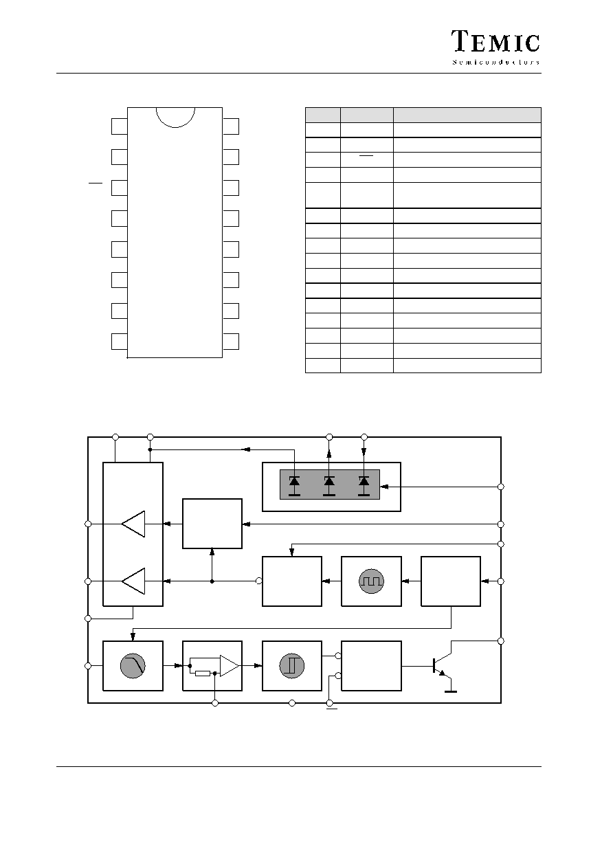
Block Diagram
Frequency
adjustment
&
&
Power supply
Driver
Low pass filter
Amplifier
= 1
Oscillator
Schmitt trigger
V
EXT
DV
S
V
S
V
Batt
COIL1
COIL2
DGND
Input
HIPASS
OE
GND
Standby
MS
CFE
RF
Output
9692
Figure 3.

U2270B
TELEFUNKEN Semiconductors
Rev. A3, 13-Dec-96
3 (13)
Functional Description
Power Supply (PS)
V
Batt
6 V
6 V
18 V
25 k
W
12 k
W
internal supply
V
S
9 V
PS
DRV
DV
S
Standby
COILx
DGND
11413
V
EXT
Figure 4. Equivalent circuit of power supply and antenna driver
The U2270 can be operated with one external supply
voltage or with two externally-stabilized supply voltages
for an extended driver output voltage or from the 12-V
battery voltage of a vehicle. The 12-V supply capability
is achieved via the on-chip power supply (see figure 4).
The power supply provides two different output voltages,
V
S
and V
EXT
.
V
S
is the internal power supply voltage except for the
driver circuit. Pin V
S
is used to connect a block capacitor.
V
S
can be switched off by the pin STANDBY. In standby
mode, the chip's power consumption is very low. V
EXT
is
the supply voltage of the antenna's pre-driver. This
voltage can also be used to operate external circuits, i.e.,
a microcontroller. In conjunction with an external NPN
transistor, it also establishes the supply voltage of the
antenna coil driver, DVS.

U2270B
TELEFUNKEN Semiconductors
Rev. A3, 13-Dec-96
4 (13)
The following section explains the 3 different
operation modes to power the U2270B.
1.
One-rail operation
All internal circuits are operated from one 5-V power rail.
(see figure 5). In this case, V
S
,V
EXT
and DV
S
serve as
inputs. V
Batt
is not used but should also be connected to
that supply rail.
D
VS
V
EXT
V
S
V
Batt
Standby
+5 V (stabilized)
12579
Figure 5.
2.
Two-rail operation
In that application, the driver voltage, DV
S,
and the
pre-driver supply, V
EXT
, are operated at a higher voltage
than the rest of the circuitry to obtain a higher
driver-output swing and thus a higher magnetic field,
refer to figure 6. V
S
is connected to a 5-V supply, whereas
the driver voltages can be as high as 8 V. This operation
mode is intended to be used in situations where an
extended communication distance is required.
D
VS
V
EXT
V
S
V
Batt
Standby
5 V (stabilized)
12580
7 to 8 V (stabilized)
Figure 6.
3.
Battery-voltage operation
Using this operation mode, V
S
and V
EXT
are generated by
the internal power supply. (refer to figure 7). For this
mode, an external voltage regulator is not needed. The IC
can be switched off via the pin Standby. V
EXT
supplies the
base of an external NPN transistor and external circuits,
i.e., a microcontroller (even in Standby mode).
Pin V
EXT
and V
Batt
are overvoltage protected via internal
Zener diodes (refer figure 4).The maximum current into
that pins is determined by the maximum power dissipa-
tion and the maximum junction temperature of the IC. For
a short-time current pulse, a higher power dissipation can
be assumed (refer to application note ANT019).
D
VS
V
EXT
V
S
V
Batt
Standby
12600
7 to 16 V
Figure 7.
Table 1. The following table summarizes the characteristics of the various operation modes.
Operation Mode
External Components Re-
quired
Supply Voltage Range
Driver Output
Voltage Swing
Standby Mode
Available
¡¡¡¡¡¡¡¡
¡
¡¡¡¡¡¡
¡
¡¡¡¡¡¡¡¡
1. One-rail operation
¡¡¡¡¡¡¡¡¡
¡
¡¡¡¡¡¡¡
¡
¡¡¡¡¡¡¡¡¡
1 Voltage regulator
1 Capacitor
¡¡¡¡¡¡¡¡
¡¡¡¡¡¡¡
¡
¡¡¡¡¡¡¡¡
5 V
±
10%
¡¡¡¡¡¡¡
¡
¡¡¡¡¡
¡
¡¡¡¡¡¡¡
[ 4 V
¡¡¡¡¡¡
¡
¡¡¡¡
¡
¡¡¡¡¡¡
No
¡¡¡¡¡¡¡¡
¡
¡¡¡¡¡¡
¡
¡¡¡¡¡¡¡¡
2. Two-rail operation
¡¡¡¡¡¡¡¡¡
¡
¡¡¡¡¡¡¡
¡
¡¡¡¡¡¡¡¡¡
2 Voltage regulators
2 Capacitors
¡¡¡¡¡¡¡¡
¡¡¡¡¡¡¡
¡
¡¡¡¡¡¡¡¡
5 V
±
10%
7 V to 8 V
¡¡¡¡¡¡¡
¡
¡¡¡¡¡
¡
¡¡¡¡¡¡¡
6 V to 7 V
¡¡¡¡¡¡
¡
¡¡¡¡
¡
¡¡¡¡¡¡
No
¡¡¡¡¡¡¡¡
¡
¡¡¡¡¡¡
¡
¡
¡¡¡¡¡¡
¡
¡
¡¡¡¡¡¡
¡
¡¡¡¡¡¡¡¡
3. Battery voltage
operation
¡¡¡¡¡¡¡¡¡
¡
¡¡¡¡¡¡¡
¡
¡
¡¡¡¡¡¡¡
¡
¡
¡¡¡¡¡¡¡
¡
¡¡¡¡¡¡¡¡¡
1 Transistor
2 Capacitors
Optional for load-dump
protection:
1 Resistor
1 Capacitor
¡¡¡¡¡¡¡¡
¡¡¡¡¡¡¡
¡
¡¡¡¡¡¡¡
¡
¡¡¡¡¡¡¡
¡
¡¡¡¡¡¡¡¡
6 V to 16 V
¡¡¡¡¡¡¡
¡
¡¡¡¡¡
¡
¡
¡¡¡¡¡
¡
¡
¡¡¡¡¡
¡
¡¡¡¡¡¡¡
[ 4 V
¡¡¡¡¡¡
¡
¡¡¡¡
¡
¡
¡¡¡¡
¡
¡
¡¡¡¡
¡
¡¡¡¡¡¡
Yes

U2270B
TELEFUNKEN Semiconductors
Rev. A3, 13-Dec-96
5 (13)
Oscillator (Osc)
The frequency of the on-chip oscillator is controlled by a
current fed into the R
F
input. An integrated compensation
circuit ensures a widly temperature and supply voltage in-
dependent frequency which is selected by a fixed resistor
between R
F
(pin 15) and V
S
(pin 14). For 125 kHz a resis-
tor value of 110 k
W is defined. For other frequencies, use
the following formula:
R
f
+ 14375
f
0
[kHz]
≠ 5 k
W
This input can be used to adjust the frequency close to the
resonance of the antenna. For more details refer to the ap-
plicatons and the application note ANT019.
V
CC
R
F
2 k
W
9695
R
f
Figure 8. Equivalent circuit of Pin R
F
Filter (LPF)
The fully-integrated low-pass filter (4th order butter-
worth) removes the remaining carrier signal and
high-frequency disturbancies after demodulation. The
upper cut-off frequency of the LPF depends on the se-
lected oscillator frequency. The typ. value is fosc/18. That
means that data rates up to fosc/25 are possible if Bi-phase
or Manchester encoding is used.
A high-pass characteristic results from the capacitive
coupling at the input Pin 4, as shown in figure 9. The input
voltage swing is limited to 2 V
pp
. For frequency response
calculation, the impedances of the signal source and LPF
input (typ. 220 k
W) have to be considered. The recom-
mended values of the input capacitor for selected data
rates are shown in the chapter "Applications".
Note:
After switching on the carrier, the dc voltage of
the coupling capacitor changes rapidly. When
the antenna voltage is stable, the LPF needs
approximately 2 ms to recover full sensitivity.
10 k
W
210 k
W
V
Bias
≠ 0.4 V
C
IN
R
S
~
~
12601
V
Bias
+ 0.4 V
V
Bias
Figure 9. Equivalent circuit of Pin Input
Amplifier (AMP)
The differential amplifier has a fixed gain, typically 30.
The HIPASS pin is used for dc decoupling. The lower
cut≠off frequency of the decoupling circuit can be
calculated as follows:
f
cut
+
1
2
p C
HP
R
i
The value of the internal resistor R
i
can be assumed to be
2.5 k
W.
Recommended values of C
HP
for selected data rates can
be found in the chapter "Applications".
+
≠
V
Ref
R
R
R
R
R
i
Schmitt
trigger
LPF
HIPASS
C
HP
12578
Figure 10. Equivalent circuit of pin HIPASS