 | –≠–ª–µ–∫—Ç—Ä–æ–Ω–Ω—ã–π –∫–æ–º–ø–æ–Ω–µ–Ω—Ç: U2320B | –°–∫–∞—á–∞—Ç—å:  PDF PDF  ZIP ZIP |
U2320B
TELEFUNKEN Semiconductors
Rev. A1, 29-May-96
1 (7)
VHF/UHF Tuner-IC
Description
This tuner IC requires a power supply of 12 V and
performs the function of two separate oscillators and
mixers, SAW-filter driver and dual state band switch.
Features
D Frequency range from 48 to 860 MHz
D Band A: balanced high impedance mixer input and
amplitude controlled oscillator
D Band B: balanced low impedance mixer input and
symmetrical oscillator
D SAW filter driver with low impedance output
D Voltage regulator for stable operating characteristics
D ESD protection on all pins except oscillator pins and
RF-inputs
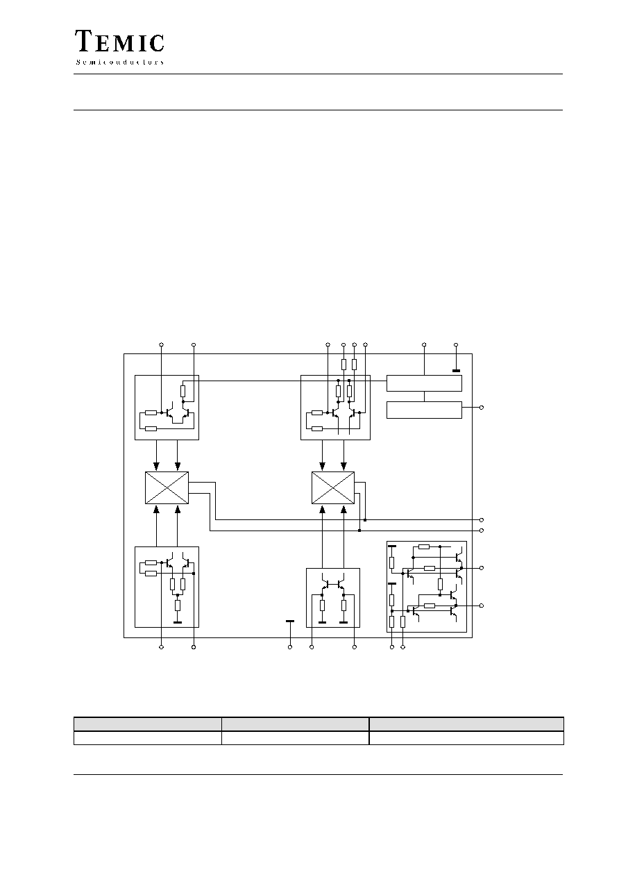
Block Diagram
RF
Osc. A
Osc. B
Voltage stabiliser
Band switch
Mixer output
SAW≠filter driver
Band A
Band B
19 18
13
14
10
9
1 3
4
15 2
20 17
16
12 11
8
95 10713
6 5 7
Figure 1.
Ordering Information
Extended Type Number
Package
Remarks
U2320B-FLG3
SO20 plastic package
Taped and reeled

U2320B
TELEFUNKEN Semiconductors
Rev. A1, 29-May-96
2 (7)
Pin Description
1
2
3
4
5
6
7
8
10
9
19
18
17
16
14
15
13
12
11
20
9612044
Osc A, base
GND (RF)
RF in, A
RF in, A
RF in, B
RF in, B
V
S
Mix.out
Mix. out
SAWF, inp.
SAWF, inp.
Osc A, coll.
Osc B, base
Osc B, coll.
Osc B, coll.
Osc B, base
Band sw.
SAWF, out
SAWF, out
GND (common)
Pin
Symbol
Function
1
Osc A, base Oscillator band A, base
2
GND
(common)
Ground, common
3
Osc A, coll. Oscillator band A, collector
4, 7
Osc B, base Oscillator band B, bases
5, 6
Osc B, coll. Oscillator band B, collectors
8
Band sw.
Dual-state band switch
9, 10
SAWF, out
SAW filter driver outputs
11, 12
SAWF, inp. SAW filter driver input
13, 14
Mix, out
Mixer outputs, open collector
15
V
S
Supply voltage V
s
16, 17
RF in, B
RF inputs, band B
18, 19
RF in, A
RF inputs, band A
20
GND (RF)
Ground, RF part
Absolute Maximum Ratings
All voltages are referred to GND, Pin 2
Parameters
Test Conditions / Pins
Symbol
Min.
Typ.
Max.
Unit
Supply voltage
Pin 15
V
S
13,.5
V
RF inputs
Pin 16-19
5.0
V
IF outputs
Pin 13-14
13. 5
V
Dual-state switch voltage
Pin 8
ViDSW
13. 5
V
Junction temperature
T
j
150
∞C
Storage temperature
T
stg
≠40
150
∞C
Operating Range
All voltages are referred to GND, Pin 2
Parameters
Test Conditions / Pins
Symbol
Min.
Typ.
Max.
Unit
Supply voltage
Pin 13-15
V
S
10.8
12
13.2
V
Ambient temperature
With heat conductive glue
T
amb
≠25
75
∞C
Thermal Resistance
Parameters
Test Conditions / Pins
Symbol
Min.
Typ.
Max.
Unit
Junction ambient
Test conditions page 4
Package soldered to PCB
R
thJA
90
K/W

U2320B
TELEFUNKEN Semiconductors
Rev. A1, 29-May-96
3 (7)
Electrical Characteristics
Test conditions (unless otherwise specified): Vs = 12 V, T
amb
= 25
∞C,
reference point Pin 2, referred to test circuit page 5.
Parameters
Test Conditions / Pins
Symbol
Min.
Typ.
Max.
Unit
Supply voltage
Pin 13-15
V
S
10.8
12.0
13.2
V
Supply current
Pin 13-15
I
S
42
50
mA
Band switch
Voltage band A
Pin 8
VSWA
0
0
1.0
V
Voltage band B
Pin 8
VSWB
3.4
4.0
5.0
V
Switching current
VSW = 5 V
Pin 8
ISW
100
mA
SAW filter driver
fi = 36 MHz
Input impedance
Pin 11, 12
ZiSAW
450
W
Output impedance
Pin 9, 10
ZoSAW
70
W
Voltage gain
11, 12
9, 10
GvSAW
19
dB
Band A (note 1)
Input frequency range
Pin18
fiA
48
470
MHz
Input impedance
Figure 4
Pin18
S11A
Gain (note 4)
I/P to O/P
GA
30
dB
Noise figure DSB (note 2)
fiA = 50 MHz
I/P to O/P
fiA = 150 MHz
NF
11.5
12
dB
dB
Input level for (note 3):
Each carrier
IM3 (Interm. of 3rd order)
fiA = 71 MHz
I/P
ViA
≠22
dBm
IM2 (Interm. of 2nd order)
fiA = 71 MHz
I/P
ViA
≠22
dBm
Band B (note 1)
Input frequency range
Pin 16, 17
fiB
470
860
MHz
Input impedance
Figure 4
Pin 16, 17
S11B
Gain (note 4)
I/P to O/P
GB
34
dB
Noise figure DSB (note 2)
fiB = 500 MHz
I/P to O/P
fiB = 800 MHz
NF
10.5
11.5
dB
dB
Input level for IM3
Each carrier
p
(Interm. of 3rd order, note 3)
fiB = 600 MHz
I/P
ViB
≠27
dBm
Notes
1)
The RF input B is symmetrical driven by means of a hybrid for 180
∞ phase shifting, consequently the source
impedance is 100
W. All other impedance for RF tests is 50 W.
2)
The noise figure (NF) is the value for double-side-band measurement.
3)
The intermodulation test (2-carrier-method) which is made on IF-centre
is in reference to a signal-to-IM ratio of 60 dB.
4
)
Gain is the ratio of the voltage at the primary coil of L5 to the available voltage at the input.

U2320B
TELEFUNKEN Semiconductors
Rev. A1, 29-May-96
4 (7)
Test and Principle Application Circuit
Bd. I/III
Hybrid 0 / 180 degree
Band B
UHF
Band A
VHF
I/P
I/P
180
15p
with 50 ohms Z(in)
and 100 ohms (2x50) Z(out)
10n
VS
SC 33.4 MHz
1n 1n
L6
IF : PC 38.9 MHz
1n 1n 1n
1n
Air Coils 0.6 mm
enamelled copper wire
L1 2 turns 2.5 mm dia
L2 8 turns 3.5 mm dia
L3 3 turns 2.5 mm dia
L4 3 turns 2.5 mm dia
TOKO≠Coils
L5 12+2 turns
L6 6+6 turns
The output voltage of the
IF is calculated back to the
primary coil of L5
IF≠Out
O/P
1n
1n
L5
15p
L3
1p0
1p0
1p0
1p0
2p2
18k
1
1k5
2p2
L1
BB515
820p
BA282
BB619
68p
L2
L4
BB515
8p2
100p
2k2
18k
1n
18k
USW
18k
VT
5
9
13
17
o
96 11674
Figure 2. Test and principle application circuit
Note:
All component values must be determined application specific. For more detailed information pls. request the
application note "Semiconductors for TV-Tuners and The New EasyLink Concept".
PCB for the R
thJA
-Measurement
95 10715
Figure 3. PCB for the R
thJA
-measurement
35
mm one-sided Cu-coated PCB,
40 mm x 40 mm x 1.5 mm.

U2320B
TELEFUNKEN Semiconductors
Rev. A1, 29-May-96
5 (7)
Input Impedance Mixer Band A (S11A) and B (S11B)
≠0.2j
≠0.5j
≠j
≠2j
≠5j
0
0.2j
0.5j
j
2j
5j
¡¡
¡¡
0.2
¡¡
¡¡
0.5
¡
¡
1
¡
¡
2
¡
¡
5
1
95 9928
¡¡¡
45 MHz
¡¡¡¡
¡¡¡¡
245 MHz
¡¡¡
¡¡¡
445 MHz
¡¡¡
645 MHz
¡¡¡¡
845 MHz
¡¡¡
1045 MHz
¡¡¡
45 MHz
¡¡¡¡
¡¡¡¡
250 MHz
¡¡¡¡
¡¡¡¡
500 MHz
¡¡¡
750 MHz
Z
0
= 50
W
1)
2)
Figure 4. Input impedance mixer band A (S11A), and B (S11B)
1)
VHF-Low
Normalized to 50
W, measuring range 45 MHz to 750 MHz.
2)
VHF-High and UHF
Normalized to 50
W, measuring range 45 MHz to 1045 MHz. Both inputs are driven symmetrical.
The output impedance of the hybrid is 100
W, the measured levels are then calculated in reference
to 50
W.