U2352B
TELEFUNKEN Semiconductors
Rev. A1, 29-May-96
1 (8)
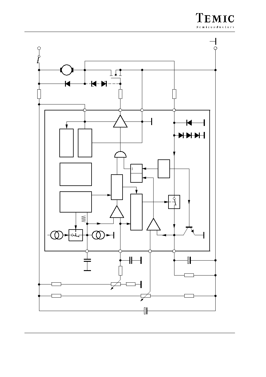
PWM Power Control for DC Loads
Description
The U2352B bipolar circuit is a PWM device for control-
ling logic level Power MOSFETs and IGBTs. It allows
simple power control for dc loads. Integrated load current
monitoring with adjustable switch-off threshold also
gives the option of measuring the load current via the
MOS transistor's on-state resistance, R
DS(on)
, or via a
shunt resistor.
Special Features
D Pulse width control up to 50 kHz clock frequency
D Load current monitoring via the on-state resistance,
R
DS(on)
, of the FET or via shunt resistor (optional)
D 100 mA push-pull output stage
D Voltage monitoring
D Temperature-compensated supply voltage limitation
D Chip temperature monitoring
Applications
D Battery-operated screwdrivers
D Battery-operated machine tools
D Halogen lamp controllers
D Dimmers
D Electronic fuses
D High-performance clock generators
Package: DIP8, SO8
Chip
temperature
monitoring
140
∞
C
Reference
voltage
Voltage
limitation 6.8 V
Oscillator
Output stage
logic
Time window
current measurement
≠
+
K1
Q
S
R
≠
+
K2
Load current
monitoring
S
2
POR
Push-pull
output stage
7
8
6
5
2 x I
GND
S
1
1
I
2
3
4
95 9670
V
S
Q
V
S
Figure 1. Block diagram

U2352B
TELEFUNKEN Semiconductors
Rev. A1, 29-May-96
3 (8)
Pin Description
1
2
3
4
8
7
6
5
Osc
V
Contr
I
Set
S
2
OUT
V
S
Output
GND
S
2
IN
95 9701
Pin
Symbol
Function
1
Osc
Oscillator
2
V
Contr
Control voltage input
3
I
Set
Setpoint value current
monitoring
4
S
2
OUT
Output, current switch S
2
5
S
2
IN
Input, current switch S
2
6
GND
Ground
7
Output
Output
8
V
S
Supply voltage
Supply, Pin 8
Internal voltage limitation in the U2352B allows a simple
supply via a series resistor R
1
. This enables operation of
the circuit under different operating voltages. Supply
voltage between Pin 8 (V
S
) and Pin 6 (GND) builds up via
R
1
and is smoothed by C
1
.
The series resistor R
1
is calculated as follows:
R
1max
+
V
Bmin
* V
Smax
I
tot
where
V
Bmin
= Minimum operating voltage
V
Smax
= Maximum supply voltage
I
tot
= I
Smax
+ I
X
I
Smax
= Maximum current consumption of the IS
I
X
= Current consumption of the external elements
Various thresholds are derived from an internal reference
voltage source.
Voltage Monitoring
During build-up and reduction of the operating voltage,
uncontrolled output pulses with excessively low ampli-
tude are suppressed by the internal monitoring circuit. All
latches are reset and the output of the load current detec-
tion Pin 4 is switched to ground.
Chip Temperature Monitoring
U2352B has integrated chip temperature monitoring
which switches off the output stage when a temperature
of approximately 140
∞
C is reached. The device is not
enabled again until cooling has taken place and the supply
voltage has been switched off and then back on again.
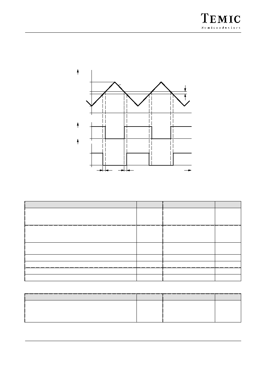
Pulse Width Control, Pins 1 and 2
At the frequency-determining capacitor, C
osc
, at Pin 1,
switching over of two internal current sources gives rise
to a triangular voltage which comparator, K
1
, compares
with the control voltage at Pin 2. If the voltage, V
1
, is
more negative than the control voltage V
2
, the output
stage is switched on via the output stage logic. When C
osc
is charged, the whole process then runs in reverse order
(see figure 3).
Load Current Monitoring, Pins 3, 4, 5
Load current can be measured with the aid of an external
shunt resistor, but this is only appropriate for decreased
loads due to additional power loss and component size
and costs. This involves the shunt voltage being fed
directly to Pin 4 via a protective resistor (see figure 5).
In order to save component costs and additional power
loss, the integrated load current monitoring allows the
load current to be directly measured via the voltage drop
at the on-state resistance, R
DS(on)
, of the FET, without an
additional shunt resistor. The drain voltage of the FET is
supplied via an external protective resistor to Pin 5.
During the off-state of the FET, a diode clamp circuit
protects the detection input, Pin 5. In the on state, the load
current flowing through the FET generates a
corresponding voltage drop at its R
DS(on)
, which is in turn
converted into a current at Pin 5 by the protective resistor.
This current reaches the integration element at Pin 4 via
the switch S
2
, which is only closed in the on-state of the
FET. If the voltage at Pin 4 exceeds the setpoint value set
at Pin 3, as a result of a high load current, the shutdown
latch is set and the output stage is blocked. To enable the
circuit again, it is necessary to switch the operating
voltage off and then back on again.
Switch-off behavior is adjusted with the resistors at Pin 4
and Pin 5 and also with the capacitor at Pin 4.
U2352B
TELEFUNKEN Semiconductors
Rev. A1, 29-May-96
4 (8)
A time space,
Dt, must be observed between switching the
output stage off and on and switching S
2
(current
measurement enable switch) in order to avoid incorrect
measurement and incorrect switching-off. To create this
time window, the control voltage V
2
is reduced internally
about
DV
2
= approximately 300 mV and the resulting
voltage, V
2
*, is compared with the triangular voltage, V
1
(see figure 3).
0.6
V
S
0.3
V
S
V
2
*
V
closed
open
Dt
V
7
V
1
DV
2
Dt
t
95 9672
S
2
V
2
Figure 3. Signal characteristics of pulse width control with time window generation
Absolute Maximum Ratings
Reference point Pin 6, unless otherwise specified
Parameters
Symbol
Value
Unit
Power supply
current
Pin 8
t < 10
ms
Pin 8
I
S
i
S
40
400
mA
Push-pull output stage
Output current
Pin 7
t < 2 ms
Pin 7
±
I
O
±
i
O
20
100
mA
Input currents
Pins 4 and 5
Pins 1 and 3
±
I
I
I
I
10
2
mA
Input voltages
Pins 1, 2 and 3
V
I
0 to V
8
V
Storage temperature range
T
stg
≠40 to +125
∞
C
Junction temperature
T
j
+125
∞
C
Ambient temperature
T
amb
≠10 to +100
∞
C
Thermal Resistance
Parameters
Symbol
Maximum
Unit
Junction ambient
DIP8
SO8 on PC board
SO8 on ceramic
R
thJA
110
220
140
K/W

U2352B
TELEFUNKEN Semiconductors
Rev. A1, 29-May-96
5 (8)
Electrical Characteristics
V
S
= 6 V, T
amb
= 25
_C, reference point Pin 6, unless otherwise specified
Parameters
Test Conditions / Pins
Symbol
Min.
Typ.
Max.
Unit
Supply voltage limitation
I
S
= 5 mA
Pin 8
I
S
= 20 mA
V
S
6.4
6.5
6.8
6.9
7.2
7.3
V
Current consumption
V
S
= 6 V
Pin 8
I
S
2.7
3.5
mA
Voltage monitoring
Switch-on threshold
Switch-off threshold
Pin 8
Pin 8
V
SON
V
SOFF
5.2
4.7
5.6
5.1
6.0
5.5
V
Oscillator
f
OSC
[kHz]
[
55
C
OSC
[nF]
V
S
[V]
Pin 1
Upper threshold (0.6
V
S
)
Lower threshold (0.3
V
S
)
Charge current
Discharge current
V
Tu
V
Tl
≠I
ch
I
dis
3.4
1.7
26
26
3.6
1.8
33
33
3.8
1.9
40
40
V
V
mA
mA
Control voltage input
Input voltage range
Input current,
Offset voltage K
1
Window, current
measurement
Pin 2
0 V
V
2
V
8
Pin 2
Pin 2≠1
Pin 2≠1
V
I
±
I
i
±
V
Offs
≠
DV
2
0
260
300
V
8
500
15
340
V
nA
mV
mV
Load current monitoring
Setpoint value input:
Input voltage range
Input current
Pin 3
0 V
V
3
6 V
Pin 3
V
I
±
I
i
0
6
500
V
nA
Offset voltage K
2
Pin 4≠3
±
V
Offs
15
mV
Load current detection:
Voltage limitation
Voltage limitation
I
5
= 1 mA
Pin 5
I
5
= ≠1 mA
Pin 5
V
L
≠V
L
2.3
0.7
V
Discharge current at POR
Pin 4
I
dis
1
mA
Switch S
2
Pin 5≠4
Residual voltage at closed
switch
V
4
= 0 V, I
5
= 50
mA
V
4
= 0.1 V, I
5
= 50
mA
V
4
= 0.3 V, I
5
= 50
mA
V
4
= 0.3 V, I
5
= 100
mA
V
Sat
175
150
125
200
mV
Push-pull output stage
Pin 7
Upper saturation voltage
I
7
= ≠2 mA
Pin 7≠8
≠V
Satu
1
V
Lower saturation voltage
I
7
= 10 mA
Pin 7
V
Satl
0.3
V
Output current
ON state
OFF state
t
2
ms
t
2
ms
≠i
o
i
o
100
100
mA