U2407B
TELEFUNKEN Semiconductors
Rev. A4, 05-Mar-97
1 (16)
Simple Controller for Fast Charge Systems
Description
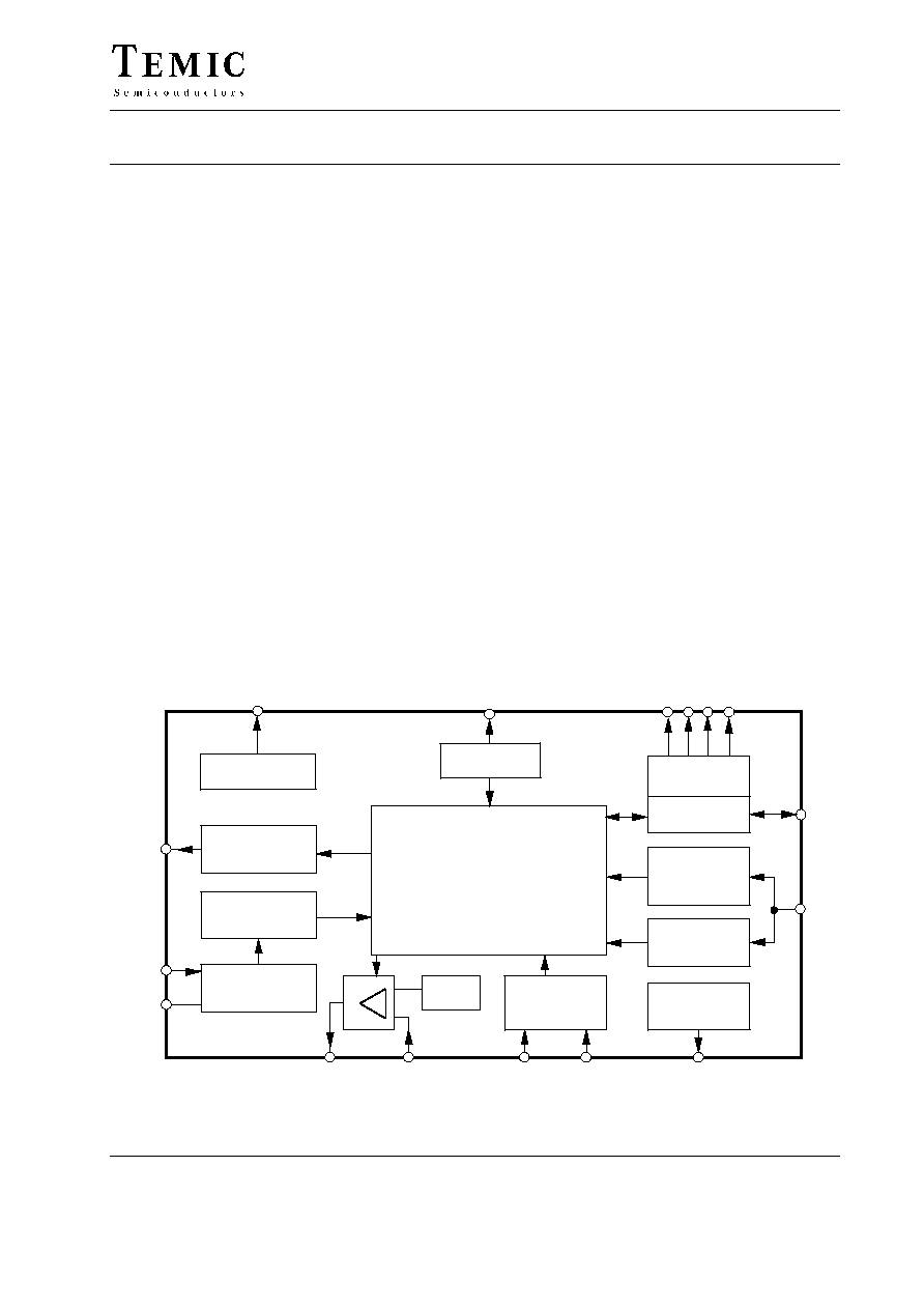
The bipolar IC U2407B is a fast charge battery controller
for drained NiCd/ NiMH batteries. Apart from phase
control, it is identical with U2405B, but has four LED
outputs. The IC enables the designer to create an efficient
and economic charge system. The U2407B incorporates
an intelligent multiple-gradient battery-voltage moni-
toring combined with temperature and failure mode
detection. With automatic top-off charging, the
integrated circuit ensures that the charge device stops
regular charging before the critical stage of overcharging
is achieved. It incorporates an additional algorithm for
reactivating fully drained batteries especially after long
time storage. It has four LED driver outputs for different
indications of the charge status.
Features
D Multiple gradient monitoring
D Temperature window (T
min
/T
max
)
D Exact currentless measurement
D Four LED status outputs
D Linear power control
D Preferred for externally regulated current sources
D Preformation algorithm for drained batteries
D Programmable top-off charge function
Applications
D Primary switch mode
D AC/ DC wall plug adapter
D Ultra fast charger (10 minutes)
Package: DIP16/ SO16
Gradient
d
2
V/dt
2
and �dV
4
2
3
Power supply
V
S
= 8 to 26 V
Switch output
Power - on control
V
Ref
6.5 V/10 mA
13
Oscillator
160 mV
Ref
Temp. control
T
max
Sensor
Battery
detection
V
Ref
= 5 V
Status control
Scan path
V
Batt
monitor
0.1 to 4 V
Charge break
output
Control unit
12
15
10
9
5
6
7
8
16
14
1
95 10648
11
Figure 1. Block diagram

U2407B
TELEFUNKEN Semiconductors
Rev. A3, 05-Mar-97
2 (16)
C
2
10
W
R
1
R
8
100 k
W
R
B2
10 k
W
R
B3
10 k
W
Output
V
Batt
Sensor
9
7
S
TM
14
V
S
C
1
1
220
mF
LED1
4
5
0.22
mF
OP
O
13
V
Ref
10
LED4
15
R
5
2.2 k
W
6
T
max
8
11
t
p
12
Osc
R
O
270 k
W
C
O
10 nF
U2407B
95 10677
OP
I
GND
C
10
10
mF
10 k
W
16
R
6
R
7
1 k
W
I
ch
1
mF
C
R
C
7
1
mF
R
sh
0.2
W
R
T2
100 k
W
R
T3
1.5 k
W
Input Voltage
8 V to 24 V
Mounted
on
heatsink
D
1
BD649
T
2
BC237
C
4
1
mF
BYW52
T
1
LED2
2
LED3
3
2.2 k
W
Battery
R
4
R
B1
1 k
W
Figure 2. Scheme for DC linear regulation
Pin Description
Package: DIP16/ SO16
LED3
OP
O
OP
I
T
max
Sensor
t
p
GND
LED2
1
2
3
4
5
6
7
8
16
15
14
13
12
11
10
9
95 10618
S
TM
Osc
V
Ref
V
S
LED4
Output
V
Batt
LED1
Pin
Symbol
Function
1
GND
Ground
2
LED2
Display output "top-off/ trickle
charge"
3
LED3
Display output "Fast charge"
4
OP
O
Operational amplifier output
5
OP
I
Operational amplifier input
6
T
max
Maximum temperature
7
Sensor
Temperature sensor
8
t
p
Charge break output
9
V
Batt
Battery voltage
10
LED1
Display output "failure mode"
11
S
TM.
Test mode switch (status control)
12
Osc
Oscillator
13
V
Ref
Reference output voltage
14
V
S
Supply voltage
15
LED4
Display output "top-off charge"
16
Output
Trigger output

U2407B
TELEFUNKEN Semiconductors
Rev. A4, 05-Mar-97
3 (16)
General Description
The integrated circuit, U2407B, is designed for charging
Nickel-Cadmium (NiCd) and Nickel-Metal-Hydride
(NiMH) batteries. Fast charging results in voltage lobes
when fully charged (figure 3). It supplies two
identifications ( i. e., + d
2
V/dt
2
,
and �
DV) to end the
charge operation at the proper time.
As compared to the existing charge concepts where the
charge is terminated
* after voltage lobes * according
to �
DV and temperature gradient identification, the
U2407B takes into consideration the additional changes
in positive charge curves, according to the second
derivative of the voltage with respect to time (d
2
V/dt
2
).
The charge identification is the sure method of switching
off the fast charge before overcharging the battery. This
helps to give the battery a long life by hindering any
marked increase in cell pressure and temperature.
Even in critical charge applications, such as a reduced
charge current or with NiMH batteries where weaker
charge characteristics are present multiple gradient
control results in very efficient switch-off.
An additional temperature control input increases not
only the performances of the charge switching
characteristics but also prevents the general charging of
a battery whose temperature is outside the specified
window.
A specific preformation algorithm is implemented for
reactivating fully drained batteries especially in the case
of batteries that have been stored for a long time.
A constant charge current is necessary for continued
charge-voltage characteristic. This constant current is
generated from an external power supply and can be regu-
lated with the help of an internal op-amp regulator
(figure 2). An external current source can also be con-
trolled by the switch output Pin 16 (see figure 12).
For further information please refer to the applications.
5 V
95 10616
Battery insertion
Fast charge stop
Top-off charge stop
Top-off
charge rate
1/4 I
O
Battery
voltage
without
charge control
preformation
t
1
= 5 min
Trickle
1/256 I
O
t
Fast charge rate I
O
t
2
= 20 min
) d
2
V
dt
2
, �
D
V
) d
2
V
dt
2
�
DV
charge rate
1.6 V
��
��
�
DV
I (R
B1)
Figure 3. Charge function diagram, f
osc
= 800 Hz

U2407B
TELEFUNKEN Semiconductors
Rev. A3, 05-Mar-97
4 (16)
Flow Chart Explanation, f
osc
= 800 Hz
(Figures 2, 3 and 4)
Battery pack insertion disables the voltage lock at battery
detection input Pin 9. All functions in the integrated
circuit are reset. For further description, DIP-pinning is
taken into consideration.
Battery Insertion and �
DV
Monitoring
After battery insertion fast charge I
o
begins when the
input voltage V
Batt
is higher than 1.6 V. For the first
5 minutes the d
2
V/dt
2
-gradient recognition is suppressed,
�
DV monitoring is activated. In case the detected V
Batt
voltage is less then 1.6 V the special preformation
procedure will be activated. The reference level with
respect to the cell voltage can be adjusted by the resistor
R
B3
(see figure 2).
Preformation Procedure
Before fast charge of fully drained or long-time stored
batteries begins, a reactivation of it is necessary. The
preformation current is dependent on pull-up resistor
R
B1
. The fast charge starts only after the V
Batt
is higher
than 1.6 V. During the first 10 minutes the green LED2 is
blinking. If after 10 minutes, V
Batt
voltage has not
reached the reference level, the indication changes to red
blinking LED1. The charge will continue with
preformation rate I (R
B1
). In case V
Batt
increases to 1.6 V
reference level, the fast charge rate current, I
o
, is
switched-on and the green LED2 is blinking.
�
DV Cut-Off (Monitoring)
When the signal at Pin 9 of the DA converter is 12 mV
below the actual value, the comparator identifies it as a
voltage drop of �
DV. The validity of �DV cut-off is
considered only if the actual value is below 12 mV for
three consecutive cycles of measurement.
d
2
V/dt
2
-Gradient
If there is no charge stop within the first 5 minutes after
battery insertion, then d
2
V/dt
2
monitoring will be active.
In this actual charge stage, all stop-charge criteria are
active.
When close to the battery's capacity limit, the battery
voltage curve will typically rise. As soon as the +d
2
V/dt
2
stop-charging criteria are met, the device will stop the fast
charge activities.
Top-Off Charge Stage
By charge disconnection through the + d
2
V/dt
2
mode, the
device switches automatically to a defined protective
top-off charge with a pulse rate of 1/4 I
O
(pulse time,
t
p
= 5.12 s, period, T = 20.48 s).
The top-off charge time is specified for a time of
20 minutes @ 800 Hz.
During top-off mode the LED4 is in ON mode.
Trickle Charge Stage
When top-off charge is terminated, the device switches
automatically to trickle charge with 1/256 I
O
(t
p
= 5.12 s,
period = 1310.72 s). The trickle continues until the
battery pack is removed.
During trickle mode the LED2 output is in on mode,
LED4 is in OFF-mode.
Basic Description
Power Supply, Figure 2
The charge controller allows the direct power supply of
8 to 26 V at Pin 14. Internal regulation limits higher input
voltages. Series resistance, R
1
, regulates the supply cur-
rent, I
S
, to a maximum value of 25 mA. Series resistance
is recommended to suppress the noise signal, even below
26 V limitation. It is calculated as follows.
R
1min
w
V
max
�26 V
25 mA
R
1max
v
V
min
� 8 V
I
tot
where
I
tot
= I
S
+ I
RB1
+ I
1
V
max,
V
min
= Rectified voltage
I
S
= Current consumption (IC) without load
I
RB1
= Current through resistance, R
B1
I
1
= Trigger current at Pin 1
