
U243B
Preliminary Information
TELEFUNKEN Semiconductors
Rev. A1, 05-Sep-96
1 (6)
Warning or Car-Direction Indicator
Technology: Bipolar
Features
D Can be protected against damage or interference with
a minimum of external circuitry
D Temperature- and voltage-compensated frequency
D Warning indication of lamp failure by means of
frequency doubling
D Voltage dependence of the car indicator lamps also
compensated for lamp failure
D Relay output with high-current carrying capacity and
low saturation voltage
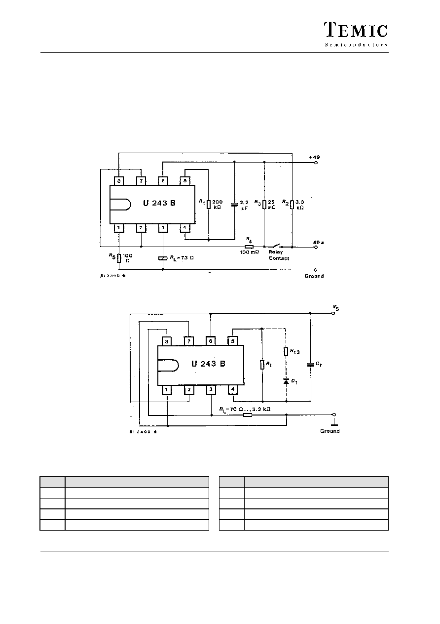
Figure 1. Application circuit as a car flasher
(Resistor R
1
, R
2
and R
t
: 1/4 Watt
R
1
for protection against continuous reversed polarity: 2 Watt)
Order Information
Extended Type Number
Package
Remarks
U243B
8 pin dual-inline plastic
U243B-FP
8 pin SO plastic

U243B
TELEFUNKEN Semiconductors
Rev. A1, 05-Sep-96
Preliminary Information
2 (6)
Circuit Description
The application circuit shows the operation of the U243B
as a car-direction indicator signal generator. The flashing
frequency is determined by the components R
t
and C
t
, and
the frequency can be calculated from
f
1
1
R
t
C
t
1.5
(Hz)
where f
1
is the frequency in normal flashing operation
(basic frequency). The control frequency f
2
is typically
2.2 times the value of f
1
and is the frequency in the case
of lamp failure. The bright periods for f
1
and f
2
are inter-
nally set in the IC and are 50% for f
1
and 40% for f
2
.
The resistors R
1
and R
2
are needed to protect the circuit
against possible damage. An integrated Z-diode in addi-
tion to these external resistors limits the impulse current
in the integrated circuit to
1.5 A. Connecting the circuit
with the wrong polarity leads to current limitation by R
1
,
R
2
and the resistance of the coil of the relay. A current of
about 150 mA would then flow over R
1
,
so that for unlim-
ited protection against continuous reversal of the polarity
of the supply, a 2-W resistor would be necessary. A short
circuit between the indicator lamp (49a) and ground (31)
can give rise to a voltage drop of about 4 V across the
measuring resistance, R
3
. The circuit is not damaged by
such a short circuit.
The use of this application circuit ensures damage and
interference protection accordance to VDE 0839. The
recognition point for lamp failure can be calculated from
the control signal threshold, typically 81 mV with
V
S
= 12 V.
With 81 mV and a measuring resistance of R
3
= 30 m
W,
it corresponds to a lamp current of 2.7 A, i.e., the
frequency change-over with a lamp load of 21 W
+ 11.4 W. The variation of the control-signal threshold
with the supply voltage takes into account the PTC char-
acteristic of the filament lamps. A resistance R
p
5 k
W
between the lamp indicator (49a) and ground (31) ensures
that in case the direction indicator switch is open, the
flashing generator is in stand-by mode.
With a control lamp of max. 4 W between 49 and 49a the
IC still starts with the bright phase.
The arrangement of the supply connections to Pins 2 and
6 must be such as to ensure that, on the connection PCB,
the resistance of V
S
to Pin 6 is lower than that to Pin 2.
Defined operation is ensured with a lamp load of
P
L
10 W or more. Defined operation with lamp loads
2
W require an additional external resistance as
described in "Applications". With considerably reduced
external circuitry, the integrated circuit U243B can be
used as an instable multivibrator in the frequency range
f = 0.05 to 10 Hz.
Absolute Maximum Ratings
Reference point Pin 1
Parameters
Symbol
Value
Unit
Supply voltage
Pins 2 and 6
V
S
16.5
V
Surge forward current
t
p
= 0.1 ms
Pins 2 and 6
I
FSM
1.5
A
t
p
= 2 ms
Pins 2 and 6
I
FSM
1.0
A
t
p
= 2 ms
Pin 8
I
FSM
50
mA
Output current
Pin 3
I
o
0.3
A
Power dissipation
T
amb
= 95
�
C
DIP8
P
tot
420
mW
SO8
P
tot
340
mW
T
amb
= 60
�
C
DIP8
P
tot
690
mW
SO8
P
tot
560
mW
Junction temperature
T
j
150
�
C
Ambient temperature range
T
amb
�40 to +95
�
C
Storage temperature range
T
stg
�55 to +125
�
C

U243B
Preliminary Information
TELEFUNKEN Semiconductors
Rev. A1, 05-Sep-96
3 (6)
Electrical Characteristics
Typical values under normal operation in application circuit figure 1, V
S
(+49, Pins 2 and 6) = 12 V
Reference point ground (�31), T
amb
= 25
�
C, unless otherwise specified
Parameters
Test Conditions / Pin
Symbol
Min
Typ
Max
Unit
Supply voltage range
Pins 2 and 6
V
S
(+49)
9 ... 15
V
Supply current,
dark phase or stand-by
Pins 2 and 6
I
S
4.5
8
mA
Supply current,
bright phase
Pins 2 and 6
I
S
7.0
11
mA
Z�diode limitation
I
S2, 6
= 70 mA
Pins 2 and 6
V
S
23
V
Relay output,
saturation voltage
I
0
= 150 mA, V
S
= 9 V
Pin 3
V
O
1.0
V
Relay output,
reverse current
Pin 3
I
O
0.1
mA
Relay coil resistance
R
L
60
W
Start delay
(first bright phase)
t
on
10
ms
Frequency-determining
resistor
R
t
6.8
510
k
W
Frequency-determining
capacitor
C
t
47
mF
Frequency tolerance (normal flashing, basic frequency
f
1
not including the tolerance of the external compo-
nents R
1
and C
t
)
f
1
�5
+5
%
Bright period
(basic frequency f
1
)
f
1
47
53
%
Bright period
(control frequency f
2
)
f
2
37
45
%
Frequency increase
(lamp failure)
f
2
2.15 f
1
2.3f
1
Control-signal threshold
V
S
= 15 V
Pin 7
V
R3
85
91
97
mV
V
S
= 9 V
Pin 7
V
R3
66
71
76
mV
V
S
= 12 V
Pin 7
V
R3
76
81
87
mV
Transfer resistance
49a to common for
stand-by
R
P
2
5
k
W
Lamp load
P
L
10
W
Applications
D Flashing generator, operation with smaller loads
(
2 W)
By adding a resistor to the application circuit (figure 1),
defined operation with lamp loads
2 W is possible. The
voltage drop across the resistor R
4
is generated by the
current flowing over the relay and should be about 15 mV.
With a relay current of 150 mA (relay resistance 73 Q),
this requires a resistance of R
4
= 100 m
W. The change of
the operating point by 15 mV results in a corresponding
change of the control signal threshold by 15 mV. For a
lamp current of 2.7 A, a measuring resistance of
R
3
=
81 mV � 15 mV
2.7 A
= 25 m
W results.
U243B
TELEFUNKEN Semiconductors
Rev. A1, 05-Sep-96
Preliminary Information
4 (6)
D Istable multivibrator
The figure shows the minimum of circuitry necessary for
the operation as an instable multivibrator. The circuit is
suitable for frequencies between 0.05 Hz and approxi-
mately 10 kHz. The frequency can be calculated by using
the relationship for f
1
given in circuit description. A start-
ing resistor of 3.8 k
W is integrated into the circuit between
pins 8 and 6. This means that, for a load on pin 3 of, for
example, 500
W (open circuits) and zero current, a voltage
of about 1.4 V remains on the load (for 70
WW the
corresponding voltage is about 220 mV). A load of R
L
3.3 k
W on pin 3 ensures correct operation of the instable
multivibrator. The relationship between the on- and off-
periods can be changed in this circuit by inserting a
resistor-diode combination parallel to R
1
(see dashed
lines in the figure), e.g., to reduce the "bright"-time.
Figure 2. Flashing generator with small loads
Figure 3. Instable multivibrator for general-purpose applications
Pin Description
Pin
Function
1
IC ground
2
Supply voltage V
S
3
Relay driver
4
C
t
oscillator
Pin
Function
5
R
t
oscillator
6
Supply voltage V
S
7
Lamp-failure detection
8
Start input (49a)
U243B
Preliminary Information
TELEFUNKEN Semiconductors
Rev. A1, 05-Sep-96
5 (6)
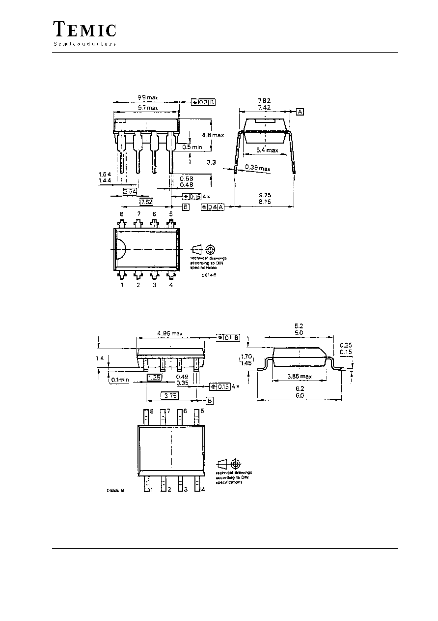
Dimensions in mm
Package: DIP8
Package: SO8 (SOT96A)

U243B
TELEFUNKEN Semiconductors
Rev. A1, 05-Sep-96
Preliminary Information
6 (6)
Ozone Depleting Substances Policy Statement
It is the policy of TEMIC TELEFUNKEN microelectronic GmbH to
1. Meet all present and future national and international statutory requirements.
2. Regularly and continuously improve the performance of our products, processes, distribution and operating systems
with respect to their impact on the health and safety of our employees and the public, as well as their impact on
the environment.
It is particular concern to control or eliminate releases of those substances into the atmosphere which are known as
ozone depleting substances ( ODSs ).
The Montreal Protocol ( 1987 ) and its London Amendments ( 1990 ) intend to severely restrict the use of ODSs and
forbid their use within the next ten years. Various national and international initiatives are pressing for an earlier ban
on these substances.
TEMIC TELEFUNKEN microelectronic GmbH semiconductor division has been able to use its policy of
continuous improvements to eliminate the use of ODSs listed in the following documents.
1. Annex A, B and list of transitional substances of the Montreal Protocol and the London Amendments respectively
2 . Class I and II ozone depleting substances in the Clean Air Act Amendments of 1990 by the Environmental
Protection Agency ( EPA ) in the USA
3. Council Decision 88/540/EEC and 91/690/EEC Annex A, B and C ( transitional substances ) respectively.
TEMIC can certify that our semiconductors are not manufactured with ozone depleting substances and do not contain
such substances.
We reserve the right to make changes to improve technical design and may do so without further notice.
Parameters can vary in different applications. All operating parameters must be validated for each customer
application by the customer. Should the buyer use TEMIC products for any unintended or unauthorized
application, the buyer shall indemnify TEMIC against all claims, costs, damages, and expenses, arising out of,
directly or indirectly, any claim of personal damage, injury or death associated with such unintended or
unauthorized use.
TEMIC TELEFUNKEN microelectronic GmbH, P.O.B. 3535, D-74025 Heilbronn, Germany
Telephone: 49 ( 0 ) 7131 67 2831, Fax number: 49 ( 0 ) 7131 67 2423