U2514B
Preliminary Information
TELEFUNKEN Semiconductors
Rev. A2, 04-Nov-96
1 (15)
AM/FM Receiver for Digital Tuning with FM-Stereo Decoder
Description
The U2514B is an integrated bipolar radio suitable for
digital tuning systems. It contains a FM front end with
pre-amplifier and FM-stereo decoder as well as a
complete AM receiver and demodulator. Stop-signal
generation is implemented for FM and AM mode. This
circuit is designed for use in small radios, power packs
and multimedia applications
Features
D FM wideband AGC
D LO-buffer for digital tuning
D Integrated stop signal generation with true
AM/ FM discriminators
D Adjustable stop signal sensitivity
D Automatic stereo-mono-blend
D High cut
D Mute function
D Pilot canceller
D Supply voltage range 3 to 12 V
D Package: SSO28
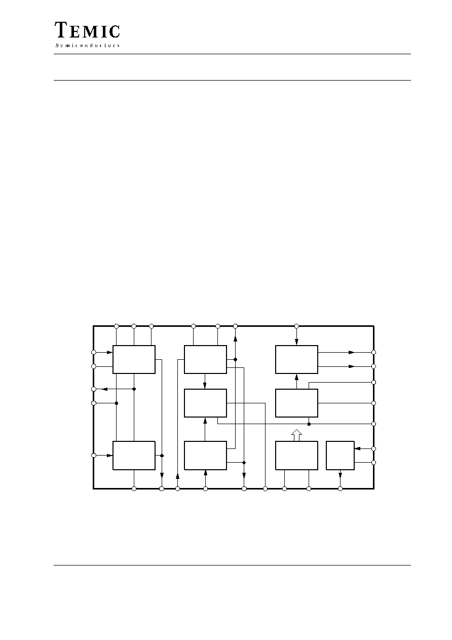
Block Diagram
FM IF +
demodulator
Matrix
decoder
+ HCC
FM front end
6
5
3
15
11
25
FMOSCE
FMOSCB
FMRF
FMDET
AFSM
MPXOUT
24
MPXIN
AM FM stop
signal detect
AM IF +
demodulator
AM front end
7
13
10
12
17
9
Pilot PLL
AMOSC
IFOUT
FMIFIN
AMIFIN
METER
AMSADJ
Control
unit
22
26
CTRLA
AMFM
V
Ref
14
VREF
27
16
23
20
21
19
18
OUTR
OUTL
LPF
CERES
GND
CTRLB
VS
28
2
8
4
1
FMIN
FMAGC
OSCOUT
GNDRF
AMIN
12305
Figure 1.

U2514B
TELEFUNKEN Semiconductors
Rev. A2, 04-Nov-96
Preliminary Information
2 (15)
Pin Description
1
2
3
4
5
6
7
8
10
9
27
22
21
20
18
19
17
12
11
28
25
26
23
24
FMOSCB
AMOSC
OSCOUT
AMSADJ
IFOUT
AFSM
GNDRF
FMOSCE
FMIFIN
FMRF
FMAGC
AMIN
CTRLB
CTRLA
LPF
CERES
OUTL
OUTR
MPXOUT
MPXIN
METER
AMFM
VS
FMIN
16
15
14
13
10547
AMIFIN
VREF
GND
FMDET
Figure 2. Pinning
Pin
Symbol
Function
1
AMIN
AM antenna input
2
FMAGC
FM-AGC time constant
3
FMRF
FM RF tank
4
GNDRF
Ground RF
5
FMOSCE FM oscillator emitter
6
FMOSCB FM oscillator basis
7
AMOSC
AM oscillator
8
OSCOUT Buffered AM/FM oscillator
output
9
AMSADJ Current-input for AM stop signal
adjust
10
IFOUT
AM/FM IF output
11
AFSM
AF smoothing voltage
12
FMIFIN
FM IF amplifier input
13
AMIFIN
AM IF amplifier input
14
VREF
Reference voltage
15
FMDET
FM discriminator output
16
GND
Ground
17
METER
Fieldstrength voltage output
18
OUTR
AF output right
19
OUTL
AF output left
20
CERES
Resonator 456 kHz
21
LPF
Low pass filter for Pilot-PLL
22
CTRLA
Control input for mute, search
mode and search sensitivity
23
CTRLB
Control input for forced mono,
control output for stop function
and stereo information
24
MPXIN
Stereo decoder MPX input
25
MPXOUT AM/FM MPX output
26
AMFM
AM/FM switch and pilot
canceller time constant
27
VS
Supply voltage
28
FMIN
FM antenna input
Ordering and Package Information
Extended Type Number
Package
Remarks
U2514B-AFN
SSO28
U2514B-AFNG3
SSO28
Taping according to ICE-286-3
U2514B
Preliminary Information
TELEFUNKEN Semiconductors
Rev. A2, 04-Nov-96
3 (15)
Pin Description
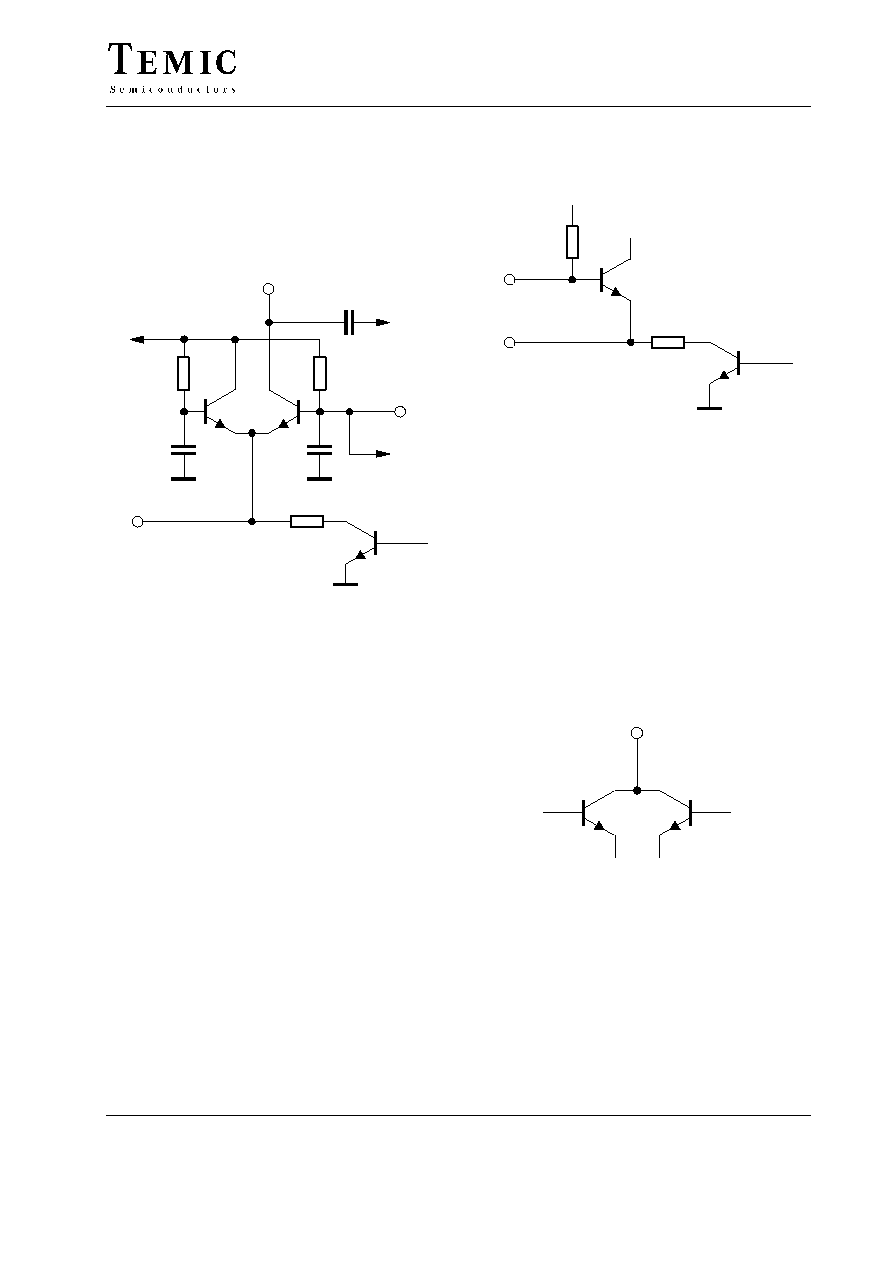
FMIN, FMAGC, FMRF
3
2
1.5 k
12414
VREF
28
FMIN
T
1
T
2
I
AGC
FMAGC
MIXER
FMRF
FM
ON
GNDRF
Figure 3.
The FM pre-amplifier input FMIN (Pin 28) consists of a
transistor grounded base circuit (T
2
) which provides
excellent noise performance and large signal behavior. It
is recommended to connect a source impedance of 100
W
in order to achieve optimal performance. The dc current
through the amplifying transitor is reduced by the internal
AGC. This means in the case of large input signals, the
input ac current is bypassed via the wideband AGC
transistor T
1
. A capacitor is connected between FMAGC
(Pin 2) and GNDRF (Pin 4). It shortens the transistor base
to GNDRF and it also serves for smoothing of the AGC
voltage. A tuned RF circuit is connected between FMRF
(Pin 3) and VS (Pin 27). The amplified RF signal is fed
internally to the mixer input.
FMOSCE, FMOSCB
12415
FM
ON
GNDRF
1.2 k
6
FMOSCB
5
FMOSCE
Figure 4.
The FM local oscillator consists of a transistor in
grounded collector configuration. The negative
resistance at the base of the transistor is generated by an
external capacitor connected between emitter FMOSCE
(Pin 5) and GNDRF (Pin 4) An other external capacitor
is connected between base FMOSCB (Pin 6) and emitter
FMOSCE (Pin 5) which increases the resistance at the
emitter and leads to a higher oscillator swing. The
negative resistance at FMOSCB is approximately 250
W.
Therefore, the resonant LO tank resistance of
approximately 5 k
W (depends on Q-factor of the coil) is
transformed to this magnitude via a capacitor.
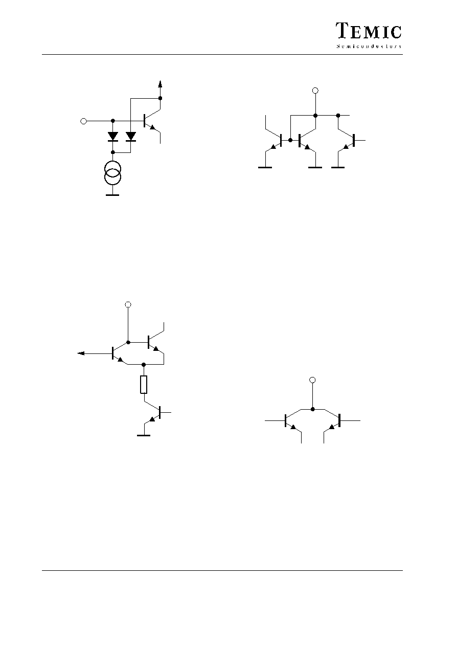
OSCOUT
12416
8
AM
FM
OSCOUT
Figure 5.
A resistor is connected between OSCOUT (Pin 8) and
VREF (Pin 14). It determines the amplitude of oscillator
voltage which is fed to the PLL circuit. The TEMIC PLL
familiy U428xBM is recommended because it offers high
signal to noise ratio and low current consumption.
U2514B
TELEFUNKEN Semiconductors
Rev. A2, 04-Nov-96
Preliminary Information
4 (15)
AMIN
12417
1
AMIN
I
AGC
GNDRF
VREF
Figure 6.
The AM antenna coil is connected between AMIN (Pin 1)
and VREF (Pin 14). In order to ensure that the AGC
operates correctly, a coil impedance of approximately 25
k
W is necessary.
AMOSC
12419
6 k
AMOSC
7
VREF
AM
ON
GNDRF
Figure 7.
The AM oscillator has to be loaded by an external tank
referred to VREF (Pin 14). If reduction of the oscillator
voltage is necessary, this may be achieved by a parallel
resistor.
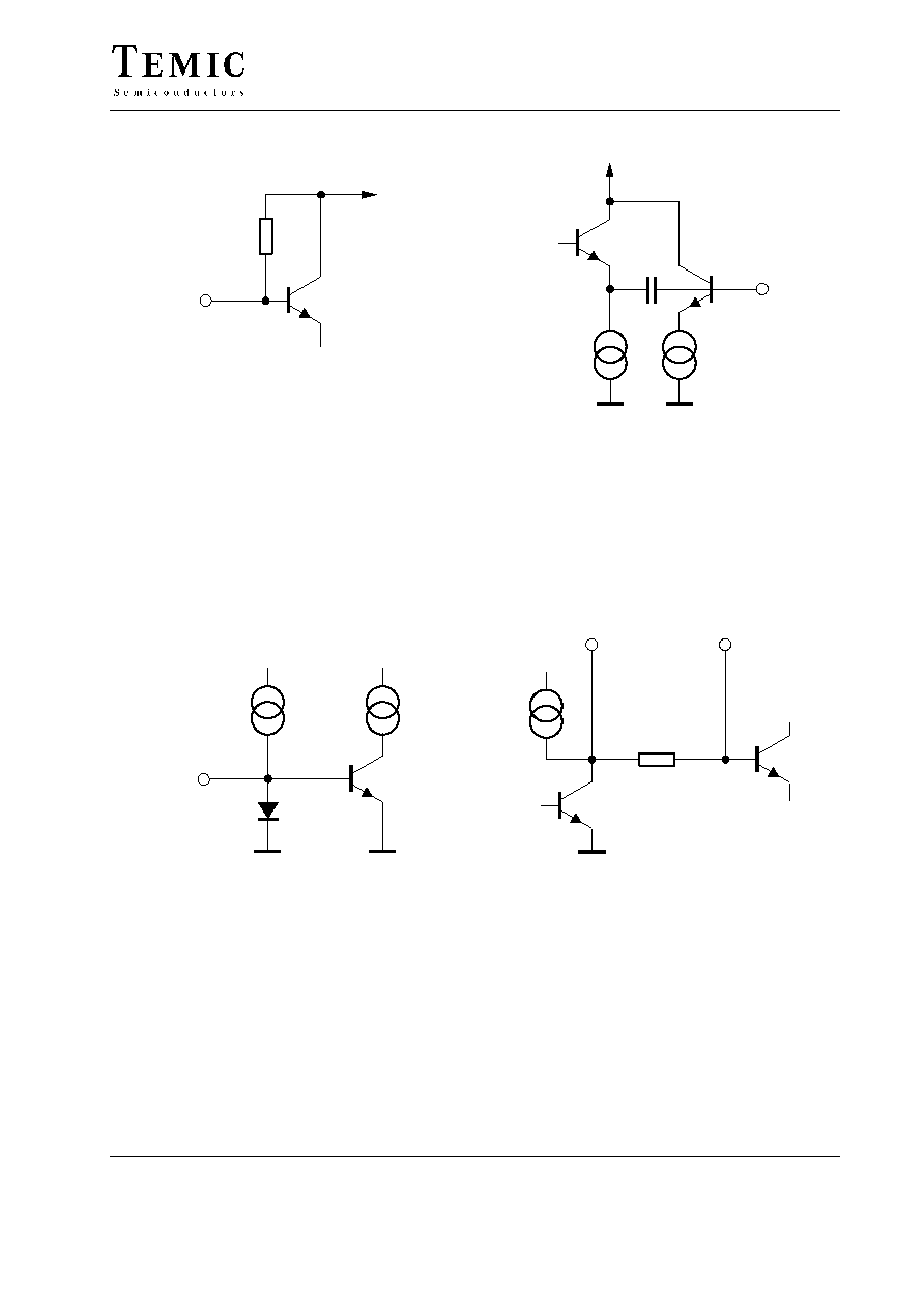
AMSADJ
12418
AMSADJ
GND
9
Figure 8.
The ceramic resonator of the stereo decoder PLL circuit
is used as a stop signal detector for AM signals. For this
purpose, the parallel resonance frequency of the
resonator, which is unloaded about 456 kHz, is reduced
by an internal load capacitor down to 455 kHz. Therefore,
the AM IF must be 455 kHz. The internal loading
capacitor is defined by the current through AMSADJ
(Pin 9) to GND. An external resistor is connected
between AMSADJ (Pin 9) and GND. It allows the
alignment of the stop signal center frequency. The width
of the stop window is typicaly 800 Hz. If AM search-
mode is not activated, the pin is internally pulled to
ground.
IFOUT
12420
10
AM
FM
IFOUT
Figure 9.
The IF output (IFOUT Pin 10) of both the FM and the AM
mixer has to be loaded into external IF-tank circuits
refered to VREF (Pin 14). Q-factor of IF coils must not be
lower than 50.
U2514B
Preliminary Information
TELEFUNKEN Semiconductors
Rev. A2, 04-Nov-96
5 (15)
AMIFIN
13
12421
3.3 k
VREF
AMIFIN
Figure 10.
The input impedance of the AM IF amplifier is 3.3 k
W
according to the required impedance of most ceramic
filters. The input refers to VREF (Pin 14).
FMIFIN
12423
12
GND
40
mA
FMIFIN
Figure 11.
The input impedance of the FM IF amplifier is 330
W
according to the required impedance of most FM ceramic
filters. The input referes to GND (Pin 16).
FMDET
12422
150
mA
15
VREF
FMDET
Figure 12.
The discriminator allows the connection of a ceramic
resonator or LC tank. A minimization of THD and
adjustment of center frequency versus temperature can
only be achieved by using a LC tank. This performs a
temperature independent stop signal.
AFSM
25
12424
100 k
11
MPXOUT
AFSM
Figure 13.
A capacitor is connected between AFSM (Pin 11) and
GND for smoothing of the FM-AF. This is necessary to
generate a modulation independent stop signal. (Because
the deviation of the FM signal (75 kHz) can be greater
than the stop signal window (25 kHz)). In the
AM-search-mode, the external capacitor smoothes the
demodulated AM-IF-signal.