 | –≠–ª–µ–∫—Ç—Ä–æ–Ω–Ω—ã–π –∫–æ–º–ø–æ–Ω–µ–Ω—Ç: U2730B-B | –°–∫–∞—á–∞—Ç—å:  PDF PDF  ZIP ZIP |

U2730B-B
Preliminary Information
Rev. A1, 22-Jul-98
1 (12)
L-Band Down-Converter for DAB Receivers
Description
The U2730B-B is a monolithic integrated L-band down-
converter circuit fabricated in TEMIC's advanced
UHF5S technology. Combining the functionality of
U2754B-B and U2755B-B in one integrated circuit, it
covers all functions of an L-band down-converter in a
DAB receiver. The device includes a gain-controlled
amplifier, a gain-controlled mixer, an output buffer, a
gain-control block, an L-band oscillator and a complete
frequency syntheziser unit. The frequency syntheziser
block consists of an input buffer for the reference
frequency signal, a reference divider, an LO divider, a
tri-state phase detector, a loop filter amplifier, a lock
detector, a programmable charge pump, a test interface
and a control interface.
Electrostatic sensitive device.
Observe precautions for handling.
Features
D Supply voltage: 8.5 V
D RF frequency range: 1400 MHz to 1550 MHz
D IF frequency range: 150 MHz to 250 MHz
D Overall IM3 rejection: > 40 dB
D Overall gain control range: typ. 30 dB
D DSB noise figure: 9.5 dB
D Gain-controlled amplifier
D Gain-controlled L-band mixer
D On-chip gain-control circuitry
D On-chip VCO, typical frequency 1261.568 MHz
D Internal VCO can be overdriven by an external LO
D On-chip frequency synthesizer
≠
Fixed LO divider factor: 2464
≠
Four reference divider factors selectable: 32, 35, 36, 48
≠
Tristate phase detector with programmable charge pump
≠
De-activation of tuning output programmable
≠
Lock-status indication
≠
Test interface
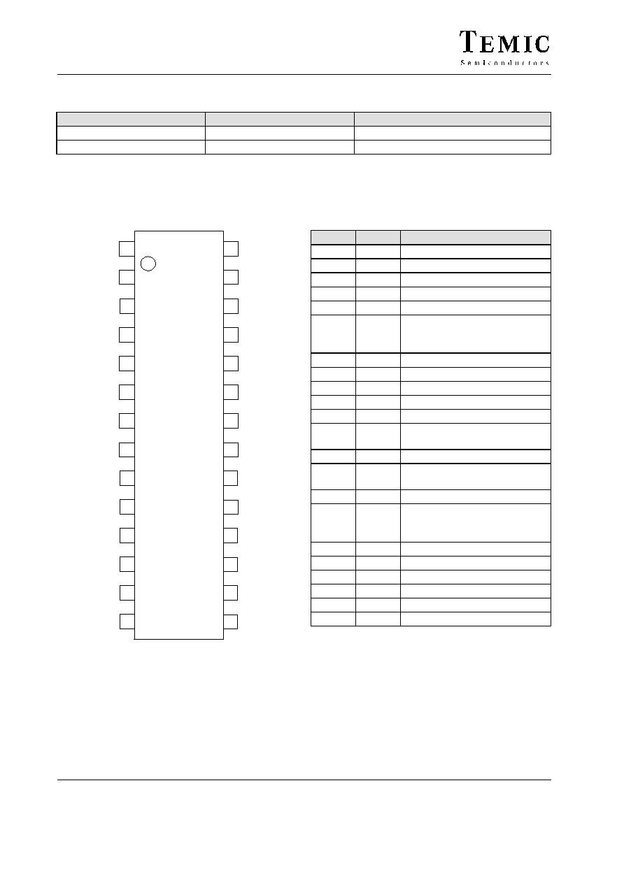
Block Diagram
14749
U
VCO
RF
26
25
NRF
18
17
Tristate
phase
detector
Reference counter
32/35/36/48
RF counter
2464
19
Test interface
10
11
Programmable
charge pump
(50
µ
A / 200
µ
A)
Control interface
Lock
detector
Voltage
stabilizer
9
6, 7, 8, 21,
22, 23, 24
12
14
13
internal supply voltage for
frequency synthesizer
TH
IF
TMD
TRD
3
VCC1
20
VCC3
28
VCC4
VCC2
GND
PLCK
PD
CD
4
5
15
16
2
27
VREF
TANK
REF
NREF
C
S
20k
AGC
Figure 1. Block diagram
U2730B-B
Rev. A1, 22-Jul-98
Preliminary Information
2 (12)
Ordering Information
Extended Type Number
Package
Remarks
U2730B-BFS
SSO28
U2730B-BFSG1
SSO28
Taped and reeled according to IEC 286≠3
Pin Description
GND
GND
VCC2
TMD
TRD
CD
PD
PLCK
1
2
3
4
5
6
7
8
10
9
27
22
21
20
18
19
17
12
11
28
25
26
23
24
GND
GND
GND
VCC3
IF
AGC
NRF
GND
TH
RF
S
VCC4
16
15
14
13
14828
NREF
REF
n.c.
C
VCC1
VREF
TANK
GND
Figure 2. Pinning
Pin
Symbol
Function
1
n.c.
Not connected
2
C
Control input
3
VCC1
Supply voltage
4
VREF
Reference pin of VCO
5
TANK
Tank pin of VCO
6, 7, 8,
21, 22,
23, 24
GND
Ground
9
VCC2
Supply voltage
10
TMD
Test output of main divider
11
TRD
Test output of reference divider
12
CD
Active filter output
13
PD
Three-state charge pump output
14
PLCK
Lock-indication output
(open collector)
15
REF
Reference divider input
16
NREF
Reference divider input
(inverted)
17
TH
Threshold voltage of comparator
18
AGC
Charge-pump output of
comparator, AGC input for
amplifier and mixer
19
IF
Intermediate frequency output
20
VCC3
Supply voltage
25
NRF
RF input (inverted)
26
RF
RF input
27
S
Control input
28
VCC4
Supply voltage
U2730B-B
Preliminary Information
Rev. A1, 22-Jul-98
3 (12)
Functional Description
The U2730B-B is an L-band down-converter circuit
covering a gain-controlled amplifier, a gain-controlled
mixer, an output buffer, a gain-control circuitry, an
L-band oscillator and a frequency synthesizer block.
Designed for applications in an DAB receiver, the
purpose of this circuit is to down-convert incoming
L-band signals in the frequency range of 1452 MHz to
1492 MHz to an IF frequency in the range of about
190 MHz to 230 MHz which can be handled by a
subsequent DAB tuner. A block diagram of this circuit is
shown in figure 1.
Gain-Controlled Amplifier
RF signals applied to the input Pin RF are amplified by a
gain-controlled amplifier. Although the complementary
Pin NRF is internally blocked, it is recommended to
block this pin additionally by an external capacitor. The
gain-control voltage is generated by an internal gain-
control circuitry. The output signal of this amplifier is fed
to a gain-controlled mixer.
Gain-Controlled Mixer and Output Buffer
The purpose of this mixer is to down-convert the L-band
signal in the frequency range of 1452 MHz to 1492 MHz
to an IF frequency in the range of about 190 MHz to
230 MHz. Like the amplifier, the gain of the mixer is
controlled by the gain-control circuitry. The IF signal is
buffered and filtered by a one-pole lowpass filter at a
3-dB frequency of about 500 MHz and then it is fed to the
single-ended output Pin IF.
Gain-Control Circuitry
The purpose of the gain-control circuitry is to measure the
signal power, to compare it with a certain power level and
to generate control voltages for the gain-controlled
amplifier and mixer. An equivalent circuit of this
functional block is shown in figure 4.
In order to meet this functionality, the output signal of the
buffer amplifier is weakly bandpass filtered (transition
range about 60 MHz to 550 MHz), rectified, lowpass
filtered and fed to a comparator whose threshold can be
defined by an external resistor, R
TH
, at Pin TH. By
varying the value of this resistor, a power threshold of
about ≠35 dBm to ≠25 dBm can be selected. In order to
achieve a good intermodulation ratio, it is recommended
to keep the power threshold below ≠30 dBm. An
appropriate application is shown in figure 3. Depending
on the selection made by the comparator, a charge pump
charges or discharges a capacitor which is applied to the
Pin
AGC. By varying this capacitor, different time
constants of the AGC loop can be realized. The voltage
arising at the Pin AGC is used to control the gain setting
of the gain-controlled amplifier and mixer. By applying
an external voltage to the Pin AGC the internal AGC loop
can be overdriven.
Voltage-Controlled Oscillator
A voltage-controlled oscillator supplies an LO signal to
the mixer. An equivalent circuit of this oscillator is shown
in figure 5. In the application circuits figures 3 and 5, a
ceramic coaxial resonator is applied to the oscillator's
Pins TANK and REF. It should be noted that the Pin REF
has to be blocked carefully. Figure 6 shows a different
application where the oscillator is overdriven by an
external oscillator. In any case, a DC path at a low
impedance must be established between the Pins TANK
and REF. The output signal of the oscillator is fed to the
LO divider block of the frequency synthesizer unit which
locks the VCO's frequency on the frequency of a
reference signal applied to the Pins REF and NREF.
Figure 7 shows the typical phase-noise performance of
the oscillator in locked state.
Overall Properties of the Signal Path
The overall gain of this circuit amounts 21 dB, the gain-
control range is about 32 dB.
Frequency Synthesizer
The frequency synthesizer block consists of an input
buffer for a reference signal, a reference divider, an LO
divider to divide the frequency of the internal oscillator,
a tristate phase detector, a lock detector, a programmable
charge pump, a loop filter amplifier, a control interface
and a test interface. The control interface is accessed by
two control pins, Pins C and S. The test interface provides
test signals which represent output signals of the
reference and the LO divider.
The purpose of this unit is to lock the frequency, f
VCO
, of
the internal VCO on the frequency, f
ref
, of the reference
signal applied to the input Pins REF and NREF by a
phase-locked loop according to the following equation:
f
VCO
= SF
f
ref
/ SF
ref
where:
SF
= 2464
SF
ref
= scaling factor of reference divider
according to the following table
Voltage at Pin S (Pin 27)
SF
ref
Ground
35
V
CC
/ 2
32
Open
48
V
CC
36
V
CC
-supply voltage
U2730B-B
Rev. A1, 22-Jul-98
Preliminary Information
4 (12)
Reference Divider
Four different scaling factors of the reference divider can
be selected by the input Pin S: 32, 35, 36, 48. Starting
from a reference oscillator frequency of 16.384 MHz/
17.92 MHz/ 18.432 MHz/ 24.576 MHz these scaling
factors result in an output frequency of the reference
divider of 512 kHz. If the input control Pin C is left open
(high-impedance state), a test signal which monitors the
output frequency of the reference divider appears at the
output Pin TRD of the test interface.
LO Divider
The LO divider is operated at the fixed division ratio
2464. Assuming the settings described in the section
`Reference divider', the oscillator's frequency is
controlled to be 1261.568 MHz in locked state, the output
frequency of the RF divider is 512 kHz. In analogy to the
reference divider, a test signal which monitors the output
frequency of the RF divider appears at the output
Pin TMD of the test interface if the input control Pin C is
left open (high-impedance state).
Phase Comparator,
Charge Pump and Loop Filter
The tristate phase detector causes the charge pump to
source or to sink current at the output Pin PD depending
on the phase relation of its input signals which are
provided by the reference and the RF divider respectively.
By means of the control Pin C, two different values of this
current can be selected, and furthermore the charge-pump
current can be switched off.
A high-gain amplifier (output Pin CD) which is
implemented to construct a loop filter, as shown in the
application circuit, can be switched off by means of the
control Pin C. In the application circuit figure 3, the loop
filter is completed by connecting the Pins PD and CD by
an appropriate RC network.
An internal lock detector checks if the phase difference of
the input signals of the phase detector is smaller than
approximately 250 ns in seven subsequent comparisons.
If a phase lock is detected, the open collector output
Pin PLCK is set to HIGH. It should be noted that the
output current of this pin must be limited by external
circuitry as it is not limited internally. If the voltage at the
control Pin C is chosen to be half the supply voltage, or
if this control pin is left open, the lock-detector function
is de-activated and the logical value of the PLCK output
is undefined.
Absolute Maximum Ratings
Parameters
Symbol
Value
Unit
Supply voltage
Pins 3, 9, 20 and 28
V
CC
≠0.3 to +9.5
V
RF input voltage
Pins 25 and 26
V
RF
750
mV
pp
Voltage at Pin AGC
Pin 18
V
AGC
0.5 to 6
V
Voltage at Pin TH
Pin 17
V
TH
≠0.3 to +4.0
V
Input voltage at Pin TANK
(internal oscillator overdriven)
Pin 5
V
TANK
1
V
pp
Current at IF output
Pin 19
I
IF
4.0
mA
Reference input voltage (diff.)
Pins 15 and 16
REF, NREF
1
V
pp
Control input voltage
Pins 1, 2 and 27
C, S
≠0.3 to +9.5
V
PLCK output current
Pin 14
I
PLCK
0.5
mA
PLCK output voltage
Pin 14
V
PLCK
≠0.3 to +5.5
V
Junction temperature
T
j
125
∞
C
Storage temperature
T
stg
≠40 to +125
∞
C
Operating Range
Parameters
Symbol
Min.
Typ.
Max.
Unit
Supply voltage
Pins 3, 9, 20 and 28
V
CC
8.0
8.5
9.35
V
Ambient temperature
T
amb
≠40
+85
∞
C
U2730B-B
Preliminary Information
Rev. A1, 22-Jul-98
5 (12)
Thermal Resistance
Parameters
Symbol
Value
Unit
Junction ambient
SSO28 (mod.)
R
thJA
t.b.d.
K/W
Electrical Characteristics
Operating conditions: V
CC
= 8.5 V, T
amb
= 25
∞
C, application circuit see figure 3, unless otherwise specified
Parameters
Test Conditions / Pins
Symbol
Min.
Typ.
Max.
Unit
Supply current (max. gain)
p
RF
= ≠60 dBm
I
S,MAX
40
51
62
mA
Supply current (min. gain)
p
RF
= ≠10 dBm
I
S,MIN
44
55
66
mA
Overall characteristics
Pin 8
2
Maximum conversion gain
p
RF
= ≠60 dBm
g
c,max
18
21
24
dB
Minimum conversion gain
p
RF
= ≠10 dBm
g
c,min
≠14
≠11
≠8
dB
AGC range
Dg
c
32
dB
Third order 2 tone
intermodulation ratio
p
RF1
+ p
RF2
= ≠6 dBm
p
RF1
+ p
RF2
= ≠15 dBm
dim3
20
30
35
40
dB
dB
DSB noise figure
(50-
system)
Maximum gain
Minimum gain
NF
9.5
30
dB
dB
RF input
Pin 26
Frequency range
f
in,RF
1400
1550
MHz
Maximum input power
dim3
20 dB
p
in,max,RF
≠6
dBm
Input impedance
Z
in,RF
200
||
1
W
||
pF
IF output
Pin 19
Frequency range
f
out,IF
150
250
MHz
Output impedance
Z
out,IF
50
Voltage standing wave ratio
VSWR
IF
2.0
VCO
Pin 5
Frequency
f
LO
1000
1261.568
1500
MHz
Phase noise
100 kHz distance, appli-
cation circuit see figure 5
L
100kHz
≠100
dBc/Hz
Minimum input power
VCO overdriven, appli-
p
LO,MIN
≠11
dBm
Maximum input power
pp
cation circuit see figure 6
p
LO,MAX
≠5
dBm
Frequency synthesizer
RF divide factor
SF
2464
Reference divide factor
Pin S connected to GND
Pin S connected to V
CC
/2
Pin S open
Pin S connected to V
CC
SF
ref
35
32
48
36