
U2740B
Preliminary Information
TELEFUNKEN Semiconductors
Rev. A3, 24-Feb-97
1 (10)
UHF AM/FM Transmitter
Description
The U2740B-B is an one-chip multi-purpose UHF
ASK/FSK transmitter IC designed for various applica-
tions within a wide frequency range. When a Chip-Select
(CS) signal is supplied, the IC starts operation (Power-up,
XTO, VCO, PD) and the VCO is then locked to
128
f(XTO). The locked status is indicated at the
Lock-Detect (LD) output.
The digital data is supplied to either an AM- or FM-input
pin, the output power being set via the AM-input pin. A
differential output enables simple applications with loop
antennas. An output driver (XTO_out) can be used for
clocking the microcontrolller.
Features
D One-chip solution with few external components
D Wide frequency range (200 to 500 MHz)
D Single voltage supply (2.2 to 5.5 V) with power-down
feature
D Adjustable output power with differential output for
loop antenna
D PLL lock-detect signal
D XTO output for
µ
C clock
D ESD protection according to MIL≠STD. 883
(except Pins 1, 2, 13 and 14)
D Low standby current <0.25 mA for V
S
= 3 V
D Single lithium-cell operation
Applications
D Keyless entry (automotive, domestic,...)
D Alarm systems
D Remote control
D Communication systems
Ordering Information
Extended Type Number
Package
Remarks
U2740B-BFP
SO16
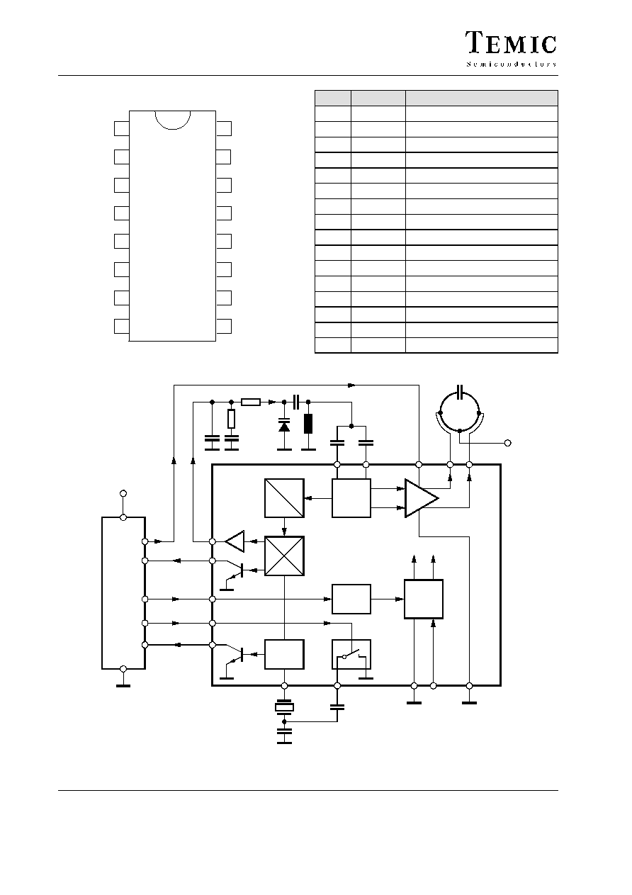
System Block Diagram
PLL
Encoder
M44Cx9x
Power
ampl.
VCO
XTO
1 Li cell
Keys
13350
U2740B
RF≠Transmitter
Antenna
Figure 1. System block diagram
U2740B
TELEFUNKEN Semiconductors
Rev. A3, 24-Feb-97
Preliminary Information
2 (10)
Pin Description
1
2
3
4
5
6
7
8
16
15
14
13
12
11
10
9
OSC1
OSC2
IC
LD
GND
FM_in
PD_out
XTAL2
AM_in
PAGND
ANT2
ANT1
V
S
CS
XTO_out
XTAL1
95 9700
Figure 2. Pinning
Pin
Symbol
Function
1
OSC1
VCO tank
2
OSC2
VCO tank
3
IC
Internally connected
4
LD
Lock-detect (open collector)
5
GND
Ground
6
FM_in
FM modulation input
7
PD_out
Phase detector output
8
XTAL2
FM modulation capacitor
9
XTAL1
XTAL
10
XTO_out
XTO output (open collector)
11
CS
Chip-select (power-up)
12
V
S
Supply voltage
13
ANT1
Differential output 1
14
ANT2
Differential output 2
15
PAGND
Power amplifier ground
16
AM_in
AM modulation input
PD
PD
LD
:128
f
Power≠up
VCO
CS
Loop
antenna
OSC1
OSC2
PA
AM_in ANT1
ANT2
Power
LD
CS
FM_in
Data
XTO_out
Clock
XTO
XTAL1
XTAL2
V
Ref
I
Ref
GND
V
S
PAGND
V
S
13324
µ
C
V
S
Figure 3. Block diagram

U2740B
Preliminary Information
TELEFUNKEN Semiconductors
Rev. A3, 24-Feb-97
3 (10)
Circuit Description
The transmitter PLL U2740B contains the complete RF
part for a radio control system. The IC consists of a VCO,
a complete PLL circuit, a crystal oscillator, a power
amplifier and a power-up module. An integrated switch
can be used to change the load capacitance of the crystal.
VCO
The VCO is a voltage-controlled current source. The
frequency is determined by the external LC-tank. The
frequency is changed via a Varicap diode.
PLL
The complete PLL consists of a prescaler, a digital
phase/frequency detector (PFD) with charge-pump
output. The output frequency is locked to 128 times the
frequency of the XTO. The PFD, however, operates at a
frequency four times lower than that of the XTO. A lock-
detect output indicates that the PLL is locked.
Crystal Oscillator (XTO)
It is a single-pin crystal oscillator, operating at the series
resonant frequency of the crystal. Depending on the type
of crystal used, this oscillator takes 3 to 20 ms until
settling after setting CS to V
S
. The integrated switch can
be used to change the load capacitance. Thus, the output
frequency is FSK modulated.
Power Amplifier (PA)
As figure 4 shows, the differential PA switches its output
current between the two power output pins (ANT1,
ANT2). The output current is seven times the current
flowing into the AM_in Pin. The achievable output power
is about 1.5 mW.
Power-up
When CS = 0 V, the circuit is in standby mode with a
power≠down supply current of type. IS,off = 0.1
µ
A. With
CS = V
S
, the circuit is in power-up mode.
PAGND
VS
ANT1
ANT2
AM_in
4.6 k
0.7 V
Iout = 3.5 mA
0.5 mA
VCO
Q1
Q2
1
7
0.7 V
Figure 4. Power output stage of U2740B

U2740B
TELEFUNKEN Semiconductors
Rev. A3, 24-Feb-97
Preliminary Information
4 (10)
Absolute Maximum Ratings
Parameters
Symbol
Min.
Max.
Unit
Supply voltage
Pin 12
V
S
≠0.3
5.5
V
Voltage at Pins 13 and 14
≠0.3
10
V
Input current AM_in
Pin 16
0.75
mA
Output current lock detect
Pin 4
1.5
mA
Output current XTO_out
Pin 10
1.5
mA
Junction temperature
T
j
125
∞
C
Storage temperature
T
stg
≠55
125
∞
C
Thermal Resistance
Parameters
Symbol
Min.
Typ.
Max.
Unit
Junction ambient
SO16
R
thJA
120
K/W
Operating Range
All voltages are referred to GND (Pin 5) and PAGND (Pin 15), T
amb
= ≠40 to +85
_C, unless otherwise specified
Parameters
Symbol
Min.
Typ.
Max.
Unit
Supply voltage
Pin 12
V
S
2.4
3.0
5.5
V
Supply voltage, T
amb
= ≠20 to +85
∞
C
V
S
2.2
3.0
5.5
V
Minimum supply voltage, T
amb
= 25
∞
C
1.8
V
Minimum supply voltage, T
amb
= ≠20
∞
C
2.0
V
Carrier frequency
200
500
MHz

U2740B
Preliminary Information
TELEFUNKEN Semiconductors
Rev. A3, 24-Feb-97
5 (10)
Electrical Characteristics DC
All voltages referred to GND (Pin 5), V
S
= 2.4 to 5.5 V, T
amb
= ≠40 to +85
∞
C, unless otherwise specified
Parameters
Test Conditions / Pins
Symbol
Min.
Typ.
Max.
Unit
Supply current
(power-down)
V
11
= 0, I
16
= 0, V
S
= 3 V
Pin 12
I
S OFF
0.05
0.25
mA
(p
)
V
11
= 0, I
16
= 0, V
S
= 5.5 V
Pin 12
I
S, OFF
0.1
0.5
mA
Supply current
V
16
= 0 V, V
11
= V
S
I
S, ON
5.0
8.0
mA
pp y
(power-up, transmit space)
V
16
= 0 V, V
11
= 3 V,
V
S
= 3 V, T
amb
= 25
∞
C,
Pin 12
I
S, ON
4.5
5.0
6.5
mA
V
16
= 0 V, V
11
= 5.5 V,
V
S
= 5.5 V, T
amb
= 25
∞
C,
Pin 12
I
S, ON
4.5
5.8
7.2
mA
Temperature coefficient of
supply current
1)
TKI
0.18
%/K
Supply current
(power-up, transmit mark)
V
16
= 3 V, V
11
= 3 V,
V
S
= 3 V, T
amb
= 25
∞
C,
Pin 12
8
11
13.5
mA
Power-down voltage
V
16
= 0 V
Pin 11
V
11, OFF
0.4
V
Power-up voltage
V
16
= 0 V
Pin 11
V
11, ON
1.0
V
Power-up current
V
11
= 3 V
Pin 11
I
11 ON
40
65
mA
p
V
11
= 5.5 V
Pin 11
I
11, ON
110
150
mA
Input current FM_in
V
6
= 3 V
Pin 6
I
6
16
25
mA
Output current
Lock-detect
Pin 4
I
4
1
Output current XTO_out
Pin 10
I
10
1
mA
Input current AM_in
2)
R16 = 0 connected to
V
S
= 3 V,
Pin 16
T
amb
= 25
∞
C
T
amb
= 85
∞
C
I
16
0.40
0.44
0.50
0.55
0.60
0.65
mA
mA
Notes:
1)
There are circuit parts with increasing supply current over temperature. The resulting supply current is
IS(T
amb
) = I
SDN
(1 + (T
amb
≠ 25
∞
C)
TKI)
2)
This depends on the value of resistor R16 connected to V
S
. If the supply voltage is 2.0 to 3.5 V, Pin 16 can
be directly connected to V
S
. For V
S
= 5 V, R16 should be 3.9 k
W.