
U2762B
Preliminary Information
Rev. A3, 10-Jun-98
1 (9)
900-MHz ISM Band Receiver
Description
The receiver IC U2762B-B is specifically designed for
cordless telephone applications in the 900-MHz ISM
band. It is manufactured using TEMIC's advanced UHF
process. The IC consists of a 900-MHz RF amplifier and
mixer, 10.7-MHz IF amplifier, limiter, RSSI, quadrature
demodulator and comparator for the bit-slicer function.
The device features 2.9-V operation. In conjunction with
TEMIC's transmitter IC U2763B-B and the PLL
U2781B, a complete ISM RF IC kit is available which fits
perfectly with AMD's PhoX controllers AM79C432A
and AM79C433.
Electrostatic sensitive device.
Observe precautions for handling.
Features
D Single-conversion receiver with 10.7-MHz IF
D Comparator for bit slicer integrated
D Temperature-compensated RSSI with 65 dB
dynamic range
D Supply-voltage range 2.7 V to 3.3 V
D Only 17 mA typical current consumption
D Few external components
D SSO28 package
Benefits
D Low filter costs due to 10.7-MHz single conversion
D Very low count of external components saves PCB
space and costs
D Low current consumption results in very long
stand-by time of approximately 7 days
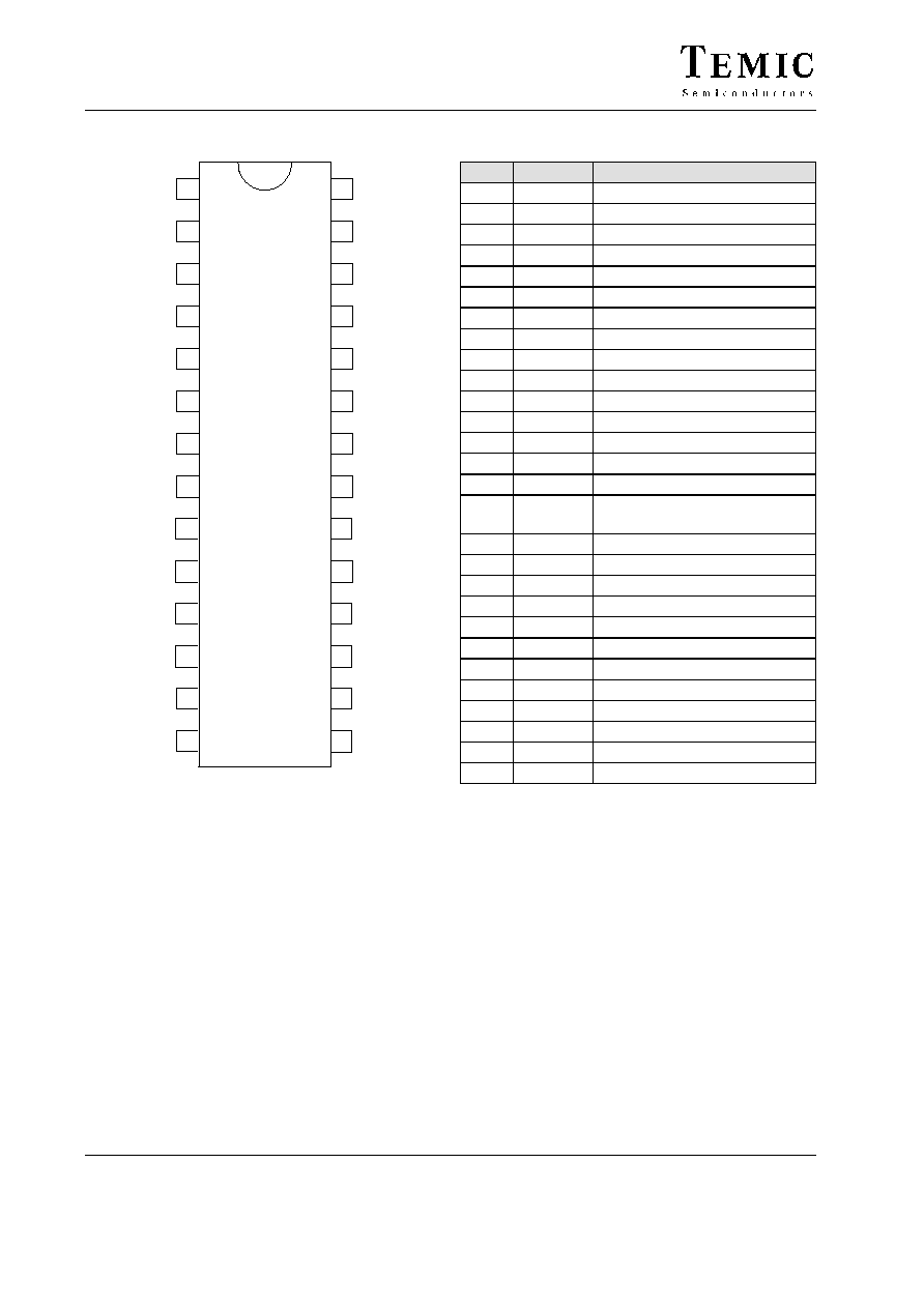
Block Diagram
28
1
2
3
4
5
6
7
8
27
26
25
24
23
22
21
9
10
11
12
13
14
20
19
18
17
16
15
V
CC1
LO
REF
LO
in
GND1
A2
out
V
CC2
Lim1
in
Lim1
REF
Lim1
out
GND3
Lim2
in
Lim2
REF
DEM
NTank
DEM
Tank
A1
REF
RSSI
NC
A1
in
GND2
Mix
out
V
CC3
A2
in
A2
REF
Data
out
Com
Nin
Com
in
SL
in
DEM
out
Compa≠
rator
Demo≠
dulator
RSSI
10 k
A2
Mix
A1
Vcc/2
+
≠
13951
Figure 1. Block diagram
Ordering Information
Extended Type Number
Package
Remarks
U2762B-BFS
SSO28
Tubes, MOQ 600 pcs
U2762B-BFSG3
SSO28
Taped and reeled, MOQ 4000 pcs
U2762B
Rev. A3, 10-Jun-98
Preliminary Information
2 (9)
Pin Description
1
2
3
4
5
6
7
8
10
9
27
22
21
20
18
19
17
12
11
28
25
26
23
24
Mix out
V
CC3
A2 in
A2 REF
Data out
Com Nin
A1 in
GND2
Com in
A1 REF
RSSI
NC
V
CC2
Lim1 in
Lim1 REF
Lim1 out
GND3
Lim2 in
GND1
A2 out
Lim2 REF
LO in
LO REF
V
CC1
16
15
14
13
13960
SL in
DEM out
DEM NTank
DEM Tank
Figure 2. Pinning
Pin
Symbol
Function
1
NC
Not connected
2
RSSI
Signal-strength indicator
3
A1 REF
RF reference
4
A1 in
RF input
5
GND2
IF ground
6
Mix out
Mixer output
7
V
CC3
IF and AF power supply
8
A2 in
IF amplifier A2 input
9
A2 REF
IF amplifier A2 reference
10
Data out
Data output
11
Com Nin
Comparator reference
12
Com in
Comparator input / slicer output
13
SL in
Slicer input
14
DEM out
Demodulator output
15
DEM Tank
Quadrature filter
16
DEM
NTank
Quadrature filter
17
Lim2 REF Limiter2 reference
18
Lim2 in
Limiter2 input
19
GND3
IF and AF Ground
20
Lim1 out
Limiter1 output
21
Lim1 REF Limiter1 reference
22
Lim1 in
Limiter1 input
23
V
CC2
IF power supply 1
24
A2 out
IF amplifier A2 output
25
GND1
RF ground
26
LO in
Local oscillator input
27
LO REF
Local oscillator reference
28
V
CC1
RF power supply
Functional Description
RF Amplifier / Mixer
The RF amplifier / mixer
down-converts the antenna
signal to the IF frequency. It has asymmetrical RF and IF
ports. The LO input includes an amplifier for good sensi-
tivity and can be used in a symmetrical- as well as an
asymmetrical configuration.
IF Amplifier A2
An additional gain stage enables an application-specific
insertion point for IF filtering.
Limiter 1 / 2
The two-stage limiting amplifier is designed to be
directly coupled to low-cost 10.7-MHz ceramic IF filters
in front of each stage. The total dynamic range is 65 dB.
Demodulator
The quadrature demodulator in the receiving path
contains an internal 7-pF quadrature capacitor to couple
the IF signal to the external tank providing the 90-degree
phase shift. The tank may be either an LC-tank circuit or
an alignment-free discrete ceramic resonator.
Bit-Slicer Amplifier and Comparator
The bit-slicer limits the baseband signal. Furthermore it
eliminates the DC-offset by an AC-coupled lowpass filter
to the demodulator output. A second lowpass filter
recovers the exact comparator threshold value of the
bit-slicer's output. The time constants of both lowpass
filters can be selected independently from each other to
optimize power-up timing.
U2762B
Preliminary Information
Rev. A3, 10-Jun-98
3 (9)
Absolute Maximum Ratings
Parameters
Symbol
Value
Unit
Supply voltage
Pins 7, 23, 28
V
CC
0 to 3.5
V
Input voltages
Pins 1, 2, 6, 10, 14, 20 and 24
V
in
0 to V
CC
V
Input voltages
Pins 3, 4, 8, 9, 11, 12, 13,15, 16,
18, 21, 22, 26 and 27
V
in
0 to V
CC
≠ 1 V
V
Junction temperature
T
j
125
_C
Storage temperature
T
stg
≠40 to +125
_C
Thermal Resistance
Parameters
Symbol
Value
Unit
Junction ambient
SSO28
R
thJA
130
K/W
Operating Range
Parameters
Symbol
Value
Unit
Supply voltage
V
S
2.7 to 3.3
V
Ambient temperature
T
amb
0 to 70
_C
Electrical Characteristics Cascaded A1 and MX1
Temperature range: 0
_C to 70_C
Parameters
Test Conditions / Pins
Symbol
Min.
Typ.
Max.
Unit
¡¡¡¡¡¡¡¡¡
¡¡¡¡¡¡¡¡¡
Supply-voltage range
¡¡¡¡¡¡¡¡¡
¡¡¡¡¡¡¡¡¡
¡¡¡¡
¡¡¡¡
V
CC
¡¡¡¡
¡¡¡¡
2.7
¡¡¡¡
¡¡¡¡
2.9
¡¡¡¡
¡¡¡¡
3.3
¡¡¡¡
¡¡¡¡
V
¡¡¡¡¡¡¡¡¡
¡¡¡¡¡¡¡¡¡
Supply current
¡¡¡¡¡¡¡¡¡
¡¡¡¡¡¡¡¡¡
Pin 28
¡¡¡¡
¡¡¡¡
I
SA1on
¡¡¡¡
¡¡¡¡
¡¡¡¡
¡¡¡¡
6.5
¡¡¡¡
¡¡¡¡
¡¡¡¡
¡¡¡¡
mA
¡¡¡¡¡¡¡¡¡
A1MX1 turn-on time
¡¡¡¡¡¡¡¡¡
¡¡¡¡
t
A1MX1on
¡¡¡¡
¡¡¡¡
2.5
¡¡¡¡
¡¡¡¡
ms
RF input impedance
Pin 4
50
W
¡¡¡¡¡¡¡¡¡
¡¡¡¡¡¡¡¡¡
RF input SWR
¡¡¡¡¡¡¡¡¡
¡¡¡¡¡¡¡¡¡
Pin 4
¡¡¡¡
¡¡¡¡
Z
A1in
¡¡¡¡
¡¡¡¡
¡¡¡¡
¡¡¡¡
< 2:1
¡¡¡¡
¡¡¡¡
¡¡¡¡
¡¡¡¡
VSWR
¡¡¡¡¡¡¡¡¡
¡¡¡¡¡¡¡¡¡
RF input frequency
¡¡¡¡¡¡¡¡¡
¡¡¡¡¡¡¡¡¡
¡¡¡¡
¡¡¡¡
f
in
¡¡¡¡
¡¡¡¡
800
¡¡¡¡
¡¡¡¡
¡¡¡¡
¡¡¡¡
1200
¡¡¡¡
¡¡¡¡
MHz
¡¡¡¡¡¡¡¡¡
¡¡¡¡¡¡¡¡¡
LO input impedance
¡¡¡¡¡¡¡¡¡
¡¡¡¡¡¡¡¡¡
Pins 26, 27
¡¡¡¡
¡¡¡¡
¡¡¡¡
¡¡¡¡
¡¡¡¡
¡¡¡¡
2
¡¡¡¡
¡¡¡¡
¡¡¡¡
¡¡¡¡
k
W
¡¡¡¡¡¡¡¡¡
¡¡¡¡¡¡¡¡¡
LO input frequency
¡¡¡¡¡¡¡¡¡
¡¡¡¡¡¡¡¡¡
¡¡¡¡
¡¡¡¡
f
LOin
¡¡¡¡
¡¡¡¡
800
¡¡¡¡
¡¡¡¡
¡¡¡¡
¡¡¡¡
1200
¡¡¡¡
¡¡¡¡
MHz
¡¡¡¡¡¡¡¡¡
¡
¡¡¡¡¡¡¡
¡
¡
¡¡¡¡¡¡¡
¡
¡¡¡¡¡¡¡¡¡
A1/MX1 cascaded
insertion voltage gain
¡¡¡¡¡¡¡¡¡
¡
¡¡¡¡¡¡¡
¡
¡
¡¡¡¡¡¡¡
¡
¡¡¡¡¡¡¡¡¡
MX1
LO
= 916.8 MHz
MX1
RF
= 927.5 MHz
P
in
= ≠40 dBm
P
LOin
= ≠20 dBm
¡¡¡¡
¡
¡¡
¡
¡
¡¡
¡
¡¡¡¡
G
VA1MX1
¡¡¡¡
¡
¡¡
¡
¡
¡¡
¡
¡¡¡¡
21
¡¡¡¡
¡
¡¡
¡
¡
¡¡
¡
¡¡¡¡
24
¡¡¡¡
¡
¡¡
¡
¡
¡¡
¡
¡¡¡¡
27
¡¡¡¡
¡
¡¡
¡
¡
¡¡
¡
¡¡¡¡
dB
¡¡¡¡¡¡¡¡¡
¡¡¡¡¡¡¡¡¡
Noise figure
¡¡¡¡¡¡¡¡¡
¡¡¡¡¡¡¡¡¡
SSB
¡¡¡¡
¡¡¡¡
N
F
¡¡¡¡
¡¡¡¡
¡¡¡¡
¡¡¡¡
11.5
¡¡¡¡
¡¡¡¡
¡¡¡¡
¡¡¡¡
dB
¡¡¡¡¡¡¡¡¡
¡¡¡¡¡¡¡¡¡
1-dB compression point
¡¡¡¡¡¡¡¡¡
¡¡¡¡¡¡¡¡¡
Input Pin 4
¡¡¡¡
¡¡¡¡
P
1dB
¡¡¡¡
¡¡¡¡
¡¡¡¡
¡¡¡¡
≠27
¡¡¡¡
¡¡¡¡
¡¡¡¡
¡¡¡¡
dBm
¡¡¡¡¡¡¡¡¡
¡¡¡¡¡¡¡¡¡
Output voltage @ 1 dB
compression
¡¡¡¡¡¡¡¡¡
¡¡¡¡¡¡¡¡¡
MX1
LO
= 916.8 MHz,
MX1
RF
= 927.5 MHz, Pin 6
¡¡¡¡
¡¡¡¡
P
1dBout
¡¡¡¡
¡¡¡¡
¡¡¡¡
¡¡¡¡
104
¡¡¡¡
¡¡¡¡
¡¡¡¡
¡¡¡¡
dB
mV
¡¡¡¡¡¡¡¡¡
¡
¡¡¡¡¡¡¡
¡
¡
¡¡¡¡¡¡¡
¡
¡
¡¡¡¡¡¡¡
¡
¡¡¡¡¡¡¡¡¡
3rd-order intercept point
¡¡¡¡¡¡¡¡¡
¡
¡¡¡¡¡¡¡
¡
¡
¡¡¡¡¡¡¡
¡
¡
¡¡¡¡¡¡¡
¡
¡¡¡¡¡¡¡¡¡
f
LO
= 980 MHz
P
LO
= ≠20 dBm
f
RF1
= 1 GHz
f
RF2
= 995 MHz
P
RF
= ≠40 dBm,
Pin 4
¡¡¡¡
¡
¡¡
¡
¡
¡¡
¡
¡
¡¡
¡
¡¡¡¡
IIP3
¡¡¡¡
¡
¡¡
¡
¡
¡¡
¡
¡
¡¡
¡
¡¡¡¡
¡¡¡¡
¡
¡¡
¡
¡
¡¡
¡
¡
¡¡
¡
¡¡¡¡
≠15
¡¡¡¡
¡
¡¡
¡
¡
¡¡
¡
¡
¡¡
¡
¡¡¡¡
¡¡¡¡
¡
¡¡
¡
¡
¡¡
¡
¡
¡¡
¡
¡¡¡¡
dBm
¡¡¡¡¡¡¡¡¡
¡¡¡¡¡¡¡¡¡
LO to RF leakage
¡¡¡¡¡¡¡¡¡
¡¡¡¡¡¡¡¡¡
P
LO
= ≠20 dBm
Pin 4
¡¡¡¡
¡¡¡¡
¡¡¡¡
¡¡¡¡
¡¡¡¡
¡¡¡¡
≠50
¡¡¡¡
¡¡¡¡
¡¡¡¡
¡¡¡¡
dBm
¡¡¡¡¡¡¡¡¡
¡¡¡¡¡¡¡¡¡
LO to IF leakage
¡¡¡¡¡¡¡¡¡
¡¡¡¡¡¡¡¡¡
P
LO
= ≠20 dBm
Pin 6
¡¡¡¡
¡¡¡¡
¡¡¡¡
¡¡¡¡
¡¡¡¡
¡¡¡¡
62
¡¡¡¡
¡¡¡¡
¡¡¡¡
¡¡¡¡
dB
mV
¡¡¡¡¡¡¡¡¡
¡¡¡¡¡¡¡¡¡
IF output impedance
¡¡¡¡¡¡¡¡¡
¡¡¡¡¡¡¡¡¡
@10.7-MHz IF
single ended
Pin 6
¡¡¡¡
¡¡¡¡
L
MX1Zout
¡¡¡¡
¡¡¡¡
¡¡¡¡
¡¡¡¡
330
¡¡¡¡
¡¡¡¡
¡¡¡¡
¡¡¡¡
W
U2762B
Rev. A3, 10-Jun-98
Preliminary Information
4 (9)
Electrical Characteristics A2
Parameters
Test Conditions / Pins
Symbol
Min.
Typ.
Max.
Unit
A2 turn-on time
t
A2on
2.5
ms
¡¡¡¡¡¡¡¡¡
¡¡¡¡¡¡¡¡¡
IF input impedance
¡¡¡¡¡¡¡¡¡
¡¡¡¡¡¡¡¡¡
@10.7 MHz
Pin 8
¡¡¡¡
¡¡¡¡
Z
MX2in
¡¡¡¡
¡¡¡¡
260
¡¡¡¡
¡¡¡¡
330
¡¡¡¡
¡¡¡¡
400
¡¡¡¡
¡¡¡¡
W
¡¡¡¡¡¡¡¡¡
¡¡¡¡¡¡¡¡¡
Input frequency
¡¡¡¡¡¡¡¡¡
¡¡¡¡¡¡¡¡¡
¡¡¡¡
¡¡¡¡
f
MX2in
¡¡¡¡
¡¡¡¡
¡¡¡¡
¡¡¡¡
10.7
¡¡¡¡
¡¡¡¡
22
¡¡¡¡
¡¡¡¡
MHz
¡¡¡¡¡¡¡¡¡
¡¡¡¡¡¡¡¡¡
Output frequency
¡¡¡¡¡¡¡¡¡
¡¡¡¡¡¡¡¡¡
Pin 24
¡¡¡¡
¡¡¡¡
f
MX2out
¡¡¡¡
¡¡¡¡
¡¡¡¡
¡¡¡¡
10.7
¡¡¡¡
¡¡¡¡
22
¡¡¡¡
¡¡¡¡
MHz
¡¡¡¡¡¡¡¡¡
¡¡¡¡¡¡¡¡¡
Gain
¡¡¡¡¡¡¡¡¡
¡¡¡¡¡¡¡¡¡
@10.7 MHz
¡¡¡¡
¡¡¡¡
G
p
¡¡¡¡
¡¡¡¡
8
¡¡¡¡
¡¡¡¡
10
¡¡¡¡
¡¡¡¡
12
¡¡¡¡
¡¡¡¡
dB
¡¡¡¡¡¡¡¡¡
¡¡¡¡¡¡¡¡¡
Noise figure
¡¡¡¡¡¡¡¡¡
¡¡¡¡¡¡¡¡¡
¡¡¡¡
¡¡¡¡
N
F
¡¡¡¡
¡¡¡¡
¡¡¡¡
¡¡¡¡
8
¡¡¡¡
¡¡¡¡
¡¡¡¡
¡¡¡¡
dB
¡¡¡¡¡¡¡¡¡
1-dB compression point
¡¡¡¡¡¡¡¡¡
Pin 8
¡¡¡¡
P
1dB
¡¡¡¡
¡¡¡¡
95
¡¡¡¡
¡¡¡¡
dB
mV
¡¡¡¡¡¡¡¡¡
¡¡¡¡¡¡¡¡¡
3rd-order intercept point
¡¡¡¡¡¡¡¡¡
¡¡¡¡¡¡¡¡¡
Pin 8
¡¡¡¡
¡¡¡¡
IIP3
¡¡¡¡
¡¡¡¡
¡¡¡¡
¡¡¡¡
112
¡¡¡¡
¡¡¡¡
¡¡¡¡
¡¡¡¡
dB
mV
¡¡¡¡¡¡¡¡¡
¡
¡¡¡¡¡¡¡
¡
¡¡¡¡¡¡¡¡¡
Output voltage @ 1 dB
compression
¡¡¡¡¡¡¡¡¡
¡
¡¡¡¡¡¡¡
¡
¡¡¡¡¡¡¡¡¡
@10.7 MHz
Pin 24
¡¡¡¡
¡
¡¡
¡
¡¡¡¡
P
1dBout
¡¡¡¡
¡
¡¡
¡
¡¡¡¡
¡¡¡¡
¡
¡¡
¡
¡¡¡¡
104
¡¡¡¡
¡
¡¡
¡
¡¡¡¡
¡¡¡¡
¡
¡¡
¡
¡¡¡¡
dB
mV
¡¡¡¡¡¡¡¡¡
¡¡¡¡¡¡¡¡¡
Output load
¡¡¡¡¡¡¡¡¡
¡¡¡¡¡¡¡¡¡
Single ended
Pin 24
¡¡¡¡
¡¡¡¡
L
MX2out
¡¡¡¡
¡¡¡¡
260
¡¡¡¡
¡¡¡¡
330
¡¡¡¡
¡¡¡¡
400
¡¡¡¡
¡¡¡¡
W
Common Electrical Characteristics IF/AF System
Parameters
Test Conditions / Pins
Symbol
Min.
Typ.
Max.
Unit
Supply-voltage range
Pins 7, 23
V
7
, V
23
2.7
2.9
3.3
V
¡¡¡¡¡¡¡¡¡
¡¡¡¡¡¡¡¡¡
Supply current
¡¡¡¡¡¡¡¡¡
¡¡¡¡¡¡¡¡¡
Pin 7
¡¡¡¡
¡¡¡¡
I
7
¡¡¡¡
¡¡¡¡
¡¡¡¡
¡¡¡¡
4.9
¡¡¡¡
¡¡¡¡
¡¡¡¡
¡¡¡¡
mA
¡¡¡¡¡¡¡¡¡
Supply current
¡¡¡¡¡¡¡¡¡
Pin 23
¡¡¡¡
I
23
¡¡¡¡
¡¡¡¡
6.0
¡¡¡¡
¡¡¡¡
mA
Electrical Characteristics RSSI/Lim1 and Lim2
Parameters
Test Conditions / Pins
Symbol
Min.
Typ.
Max.
Unit
¡¡¡¡¡¡¡¡¡
¡
¡¡¡¡¡¡¡
¡
¡
¡¡¡¡¡¡¡
¡
¡¡¡¡¡¡¡¡¡
≠3 dB limiting at Lim1
input
¡¡¡¡¡¡¡¡¡
¡
¡¡¡¡¡¡¡
¡
¡
¡¡¡¡¡¡¡
¡
¡¡¡¡¡¡¡¡¡
Valid for ≠5 dB insertion
loss for 2nd IF filter
Pin 22
¡¡¡¡
¡
¡¡
¡
¡
¡¡
¡
¡¡¡¡
P
3dB
¡¡¡¡
¡
¡¡
¡
¡
¡¡
¡
¡¡¡¡
¡¡¡¡
¡
¡¡
¡
¡
¡¡
¡
¡¡¡¡
¡¡¡¡
¡
¡¡
¡
¡
¡¡
¡
¡¡¡¡
8
¡¡¡¡
¡
¡¡
¡
¡
¡¡
¡
¡¡¡¡
dB
mV
Lim1/Lim2 cascaded
voltage gain
f
IF
= 10.7 MHz,
P
IFin
= ≠110 dBm
G
LIM12
110
dB
¡¡¡¡¡¡¡¡¡¡¡¡¡¡¡¡¡¡¡¡¡¡¡¡¡¡¡¡¡¡¡¡
¡¡¡¡¡¡¡¡¡¡¡¡¡¡¡¡¡¡¡¡¡¡¡¡¡¡¡¡¡¡¡¡
Limiter 1
¡¡¡¡¡¡¡¡¡
¡¡¡¡¡¡¡¡¡
Lim1 input impedance
¡¡¡¡¡¡¡¡¡
¡¡¡¡¡¡¡¡¡
Pin 22
¡¡¡¡
¡¡¡¡
Z
LIM1in
¡¡¡¡
¡¡¡¡
260
¡¡¡¡
¡¡¡¡
330
¡¡¡¡
¡¡¡¡
400
¡¡¡¡
¡¡¡¡
W
¡¡¡¡¡¡¡¡¡
¡¡¡¡¡¡¡¡¡
Lim1 input frequency
¡¡¡¡¡¡¡¡¡
¡¡¡¡¡¡¡¡¡
Pin 22
¡¡¡¡
¡¡¡¡
f
LIM1BW
¡¡¡¡
¡¡¡¡
1
¡¡¡¡
¡¡¡¡
¡¡¡¡
¡¡¡¡
22
¡¡¡¡
¡¡¡¡
MHz
¡¡¡¡¡¡¡¡¡
¡¡¡¡¡¡¡¡¡
Lim1 output impedance
¡¡¡¡¡¡¡¡¡
¡¡¡¡¡¡¡¡¡
Pin 22
¡¡¡¡
¡¡¡¡
f
LIM1out
¡¡¡¡
¡¡¡¡
260
¡¡¡¡
¡¡¡¡
330
¡¡¡¡
¡¡¡¡
400
¡¡¡¡
¡¡¡¡
W
¡¡¡¡¡¡¡¡¡
¡¡¡¡¡¡¡¡¡
Voltage gain
¡¡¡¡¡¡¡¡¡
¡¡¡¡¡¡¡¡¡
¡¡¡¡
¡¡¡¡
G
LIM1
¡¡¡¡
¡¡¡¡
¡¡¡¡
¡¡¡¡
45
¡¡¡¡
¡¡¡¡
¡¡¡¡
¡¡¡¡
dB
¡¡¡¡¡¡¡¡¡¡¡¡¡¡¡¡¡¡¡¡¡¡¡¡¡¡¡¡¡¡¡¡
¡¡¡¡¡¡¡¡¡¡¡¡¡¡¡¡¡¡¡¡¡¡¡¡¡¡¡¡¡¡¡¡
Limiter 2
¡¡¡¡¡¡¡¡¡
Lim2 input impedance
¡¡¡¡¡¡¡¡¡
Pin 18
¡¡¡¡
Z
LIM2in
¡¡¡¡
260
¡¡¡¡
330
¡¡¡¡
400
¡¡¡¡
W
¡¡¡¡¡¡¡¡¡
¡¡¡¡¡¡¡¡¡
Lim2 input frequency
¡¡¡¡¡¡¡¡¡
¡¡¡¡¡¡¡¡¡
Pin 18
¡¡¡¡
¡¡¡¡
f
LIM2BW
¡¡¡¡
¡¡¡¡
1
¡¡¡¡
¡¡¡¡
¡¡¡¡
¡¡¡¡
22
¡¡¡¡
¡¡¡¡
MHz
¡¡¡¡¡¡¡¡¡¡¡¡¡¡¡¡¡¡¡¡¡¡¡¡¡¡¡¡¡¡¡¡
¡¡¡¡¡¡¡¡¡¡¡¡¡¡¡¡¡¡¡¡¡¡¡¡¡¡¡¡¡¡¡¡
RSSI
Dynamic range
D
RSSI
20
85
dB
mV
Output voltage
@ 20 dB
mV
@ 85 dB
mV
V
out
0.1
1.7
0.2
1.8
0.3
1.9
V
V
¡¡¡¡¡¡¡¡¡
¡¡¡¡¡¡¡¡¡
RSSI fall time
¡¡¡¡¡¡¡¡¡
¡¡¡¡¡¡¡¡¡
Pin 2
¡¡¡¡
¡¡¡¡
t
fRSSI
¡¡¡¡
¡¡¡¡
¡¡¡¡
¡¡¡¡
¡¡¡¡
¡¡¡¡
50
¡¡¡¡
¡¡¡¡
ms
¡¡¡¡¡¡¡¡¡
RSSI rise time
¡¡¡¡¡¡¡¡¡
Pin 2
¡¡¡¡
t
rRSSI
¡¡¡¡
¡¡¡¡
¡¡¡¡
50
¡¡¡¡
ms
¡¡¡¡¡¡¡¡¡
¡¡¡¡¡¡¡¡¡
Output impedance
¡¡¡¡¡¡¡¡¡
¡¡¡¡¡¡¡¡¡
Pin 2
¡¡¡¡
¡¡¡¡
Z
RSSI
¡¡¡¡
¡¡¡¡
¡¡¡¡
¡¡¡¡
10 || 3
¡¡¡¡
¡¡¡¡
¡¡¡¡
¡¡¡¡
k
W || pF
U2762B
Preliminary Information
Rev. A3, 10-Jun-98
5 (9)
Electrical Characteristics Demodulator
Parameters
Test Conditions / Pins
Symbol
Min.
Typ.
Max.
Unit
¡¡¡¡¡¡¡¡¡
¡¡¡¡¡¡¡¡¡
Demodulator 3 db BW
¡¡¡¡¡¡¡¡¡
¡¡¡¡¡¡¡¡¡
Pin 14
¡¡¡¡
¡¡¡¡
f
DEMODBW
¡¡¡¡
¡¡¡¡
¡¡¡¡
¡¡¡¡
200
¡¡¡¡
¡¡¡¡
¡¡¡¡
¡¡¡¡
kHz
¡¡¡¡¡¡¡¡¡
¡
¡¡¡¡¡¡¡
¡
¡
¡¡¡¡¡¡¡
¡
¡¡¡¡¡¡¡¡¡
Demodulator total
harmonic distortion
¡¡¡¡¡¡¡¡¡
¡
¡¡¡¡¡¡¡
¡
¡
¡¡¡¡¡¡¡
¡
¡¡¡¡¡¡¡¡¡
f
mod
= 36 kHz
f
dev
= 40 kHz Pin 14
f
IFin
= 10.7 MHz
¡¡¡¡
¡
¡¡
¡
¡
¡¡
¡
¡¡¡¡
THD
¡¡¡¡
¡
¡¡
¡
¡
¡¡
¡
¡¡¡¡
¡¡¡¡
¡
¡¡
¡
¡
¡¡
¡
¡¡¡¡
< 3
¡¡¡¡
¡
¡¡
¡
¡
¡¡
¡
¡¡¡¡
¡¡¡¡
¡
¡¡
¡
¡
¡¡
¡
¡¡¡¡
%
¡¡¡¡¡¡¡¡¡
¡
¡¡¡¡¡¡¡
¡
¡¡¡¡¡¡¡¡¡
Demodulator output
voltage
¡¡¡¡¡¡¡¡¡
¡
¡¡¡¡¡¡¡
¡
¡¡¡¡¡¡¡¡¡
f
mod
= 36 kHz
f
dev
= 40 kHz Pin 14
f
IFin
= 10.7 MHz
¡¡¡¡
¡
¡¡
¡
¡¡¡¡
V
Dout
¡¡¡¡
¡
¡¡
¡
¡¡¡¡
¡¡¡¡
¡
¡¡
¡
¡¡¡¡
150
¡¡¡¡
¡
¡¡
¡
¡¡¡¡
¡¡¡¡
¡
¡¡
¡
¡¡¡¡
mV
rms
¡¡¡¡¡¡¡¡¡
¡¡¡¡¡¡¡¡¡
DC output voltage
¡¡¡¡¡¡¡¡¡
¡¡¡¡¡¡¡¡¡
Pin 14
¡¡¡¡
¡¡¡¡
¡¡¡¡
¡¡¡¡
¡¡¡¡
¡¡¡¡
1.5
¡¡¡¡
¡¡¡¡
¡¡¡¡
¡¡¡¡
V
¡¡¡¡¡¡¡¡¡
¡¡¡¡¡¡¡¡¡
Output load
¡¡¡¡¡¡¡¡¡
¡¡¡¡¡¡¡¡¡
Pin 14
¡¡¡¡
¡¡¡¡
L
Dout
¡¡¡¡
¡¡¡¡
10
¡¡¡¡
¡¡¡¡
¡¡¡¡
¡¡¡¡
¡¡¡¡
¡¡¡¡
k
W
Electrical Characteristics Comparator
Parameters
Test Conditions / Pins
Symbol
Min.
Typ.
Max.
Unit
¡¡¡¡¡¡¡¡¡
¡¡¡¡¡¡¡¡¡
Ref. input impedance
¡¡¡¡¡¡¡¡¡
¡¡¡¡¡¡¡¡¡
Pin 11
¡¡¡¡
¡¡¡¡
Z
COMPin
¡¡¡¡
¡¡¡¡
¡¡¡¡
¡¡¡¡
100
¡¡¡¡
¡¡¡¡
¡¡¡¡
¡¡¡¡
k
W
¡¡¡¡¡¡¡¡¡
¡¡¡¡¡¡¡¡¡
Output voltage `high'
¡¡¡¡¡¡¡¡¡
¡¡¡¡¡¡¡¡¡
R
LOAD
> 10 k
W
Pin 10
¡¡¡¡
¡¡¡¡
V
outH
¡¡¡¡
¡¡¡¡
V
CC
≠0.3
¡¡¡¡
¡¡¡¡
¡¡¡¡
¡¡¡¡
¡¡¡¡
¡¡¡¡
V
¡¡¡¡¡¡¡¡¡
¡¡¡¡¡¡¡¡¡
Output voltage `low'
¡¡¡¡¡¡¡¡¡
¡¡¡¡¡¡¡¡¡
R
LOAD
> 10 k
W
Pin 10
¡¡¡¡
¡¡¡¡
V
outL
¡¡¡¡
¡¡¡¡
¡¡¡¡
¡¡¡¡
¡¡¡¡
¡¡¡¡
0.3
¡¡¡¡
¡¡¡¡
V
¡¡¡¡¡¡¡¡¡
¡¡¡¡¡¡¡¡¡
Output low-to-high
rise time
¡¡¡¡¡¡¡¡¡
¡¡¡¡¡¡¡¡¡
R
LOAD
=
10 k
W Pin 10
C
LOAD
=
10 pf
¡¡¡¡
¡¡¡¡
t
r
¡¡¡¡
¡¡¡¡
¡¡¡¡
¡¡¡¡
¡¡¡¡
¡¡¡¡
500
¡¡¡¡
¡¡¡¡
ns
¡¡¡¡¡¡¡¡¡
¡
¡¡¡¡¡¡¡
¡
¡¡¡¡¡¡¡¡¡
Output high-to-low
fall time
¡¡¡¡¡¡¡¡¡
¡
¡¡¡¡¡¡¡
¡
¡¡¡¡¡¡¡¡¡
R
LOAD
=
10 k
W Pin 10
C
LOAD
=
10 pf
¡¡¡¡
¡
¡¡
¡
¡¡¡¡
t
f
¡¡¡¡
¡
¡¡
¡
¡¡¡¡
¡¡¡¡
¡
¡¡
¡
¡¡¡¡
¡¡¡¡
¡
¡¡
¡
¡¡¡¡
500
¡¡¡¡
¡
¡¡
¡
¡¡¡¡
ns
¡¡¡¡¡¡¡¡¡
¡¡¡¡¡¡¡¡¡
Hysteresis
¡¡¡¡¡¡¡¡¡
¡¡¡¡¡¡¡¡¡
Pin 12
¡¡¡¡
¡¡¡¡
V
HYST
¡¡¡¡
¡¡¡¡
¡¡¡¡
¡¡¡¡
25
¡¡¡¡
¡¡¡¡
¡¡¡¡
¡¡¡¡
mV
Electrical Characteristics Slicer Amplifier
Parameters
Test Conditions / Pins
Symbol
Min.
Typ.
Max.
Unit
¡¡¡¡¡¡¡¡¡
¡¡¡¡¡¡¡¡¡
Open loop gain
¡¡¡¡¡¡¡¡¡
¡¡¡¡¡¡¡¡¡
Pin 13 to 12
¡¡¡¡
¡¡¡¡
G
Sol
¡¡¡¡
¡¡¡¡
¡¡¡¡
¡¡¡¡
40
¡¡¡¡
¡¡¡¡
¡¡¡¡
¡¡¡¡
dB
¡¡¡¡¡¡¡¡¡
¡¡¡¡¡¡¡¡¡
Output load
¡¡¡¡¡¡¡¡¡
¡¡¡¡¡¡¡¡¡
AC load
Pin 12
¡¡¡¡
¡¡¡¡
L
Sout
¡¡¡¡
¡¡¡¡
10
¡¡¡¡
¡¡¡¡
¡¡¡¡
¡¡¡¡
¡¡¡¡
¡¡¡¡
k
W
¡¡¡¡¡¡¡¡¡
¡¡¡¡¡¡¡¡¡
Output swing
¡¡¡¡¡¡¡¡¡
¡¡¡¡¡¡¡¡¡
Pin 12
¡¡¡¡
¡¡¡¡
¡¡¡¡
¡¡¡¡
¡¡¡¡
¡¡¡¡
0.7
¡¡¡¡
¡¡¡¡
¡¡¡¡
¡¡¡¡
V
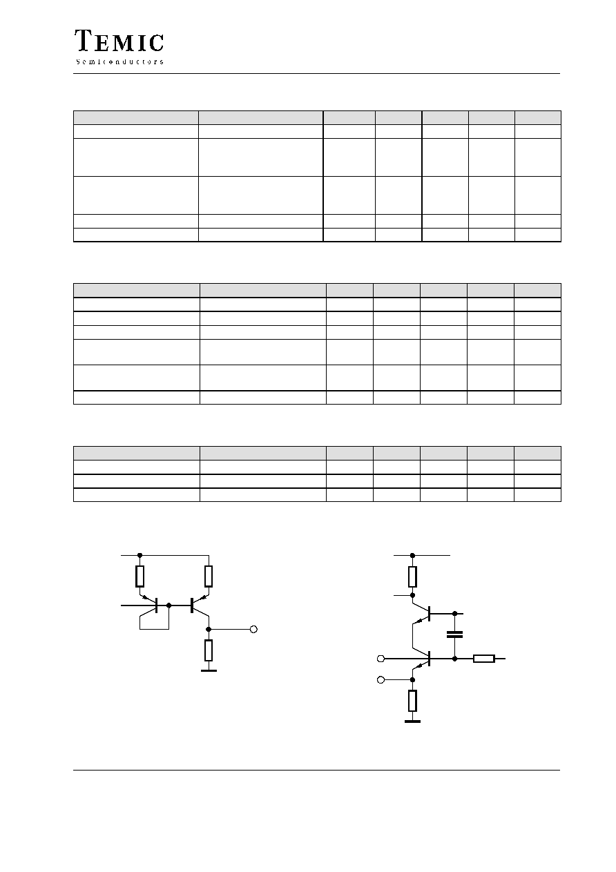
Internal Pin Configuration
13956
5 k
1 k
10 k
V
CC
2
Figure 3. Pin 2: Signal strength indicator (RSSI)
13957
V
CC
3.3 pF
1 k
3
4
800
Figure 4. Pins 3/4: RF reference / RF input