U2781B
TELEFUNKEN Semiconductors
Rev. A3, 26-Nov-97
1 (10)
Frequency Synthesizer
Description
The programmable frequency synthesizer IC U2781B for
µ
P-controlled application is realized with TEMIC's
advanced UHF process which is very suitable for
combinations of fast ECL logic and low-current I
2
L logic.
The benefits are high input sensitivity in connection with
low power consumption and therefore small
packages (SSO20). This makes the device a perfect
choice for cordless phones and handheld cellular radio
sets up to 1.1 GHz.
Electrostatic sensitive device.
Observe precautions for handling.
Features
D Very low current consumption (typ. 3 V/ 5 mA)
D Supply voltage range: 2.7 to 5.5 V
D Max. input frequency: 1.1 GHz
D Programmable prescaler 64/ 65 or 128/ 129
D Controlled by 3-wire bus with f
clock
up to 500 kHz
D Status output for PLL lock/ unlock condition
D Very fast phase detector
D SSO20 package
D ESD protection in accordance with MIL-STD. 883
method 3015 class 2
Benefits
D Very low current consumption extends talk time
D Few external components and SSO package save costs
and space
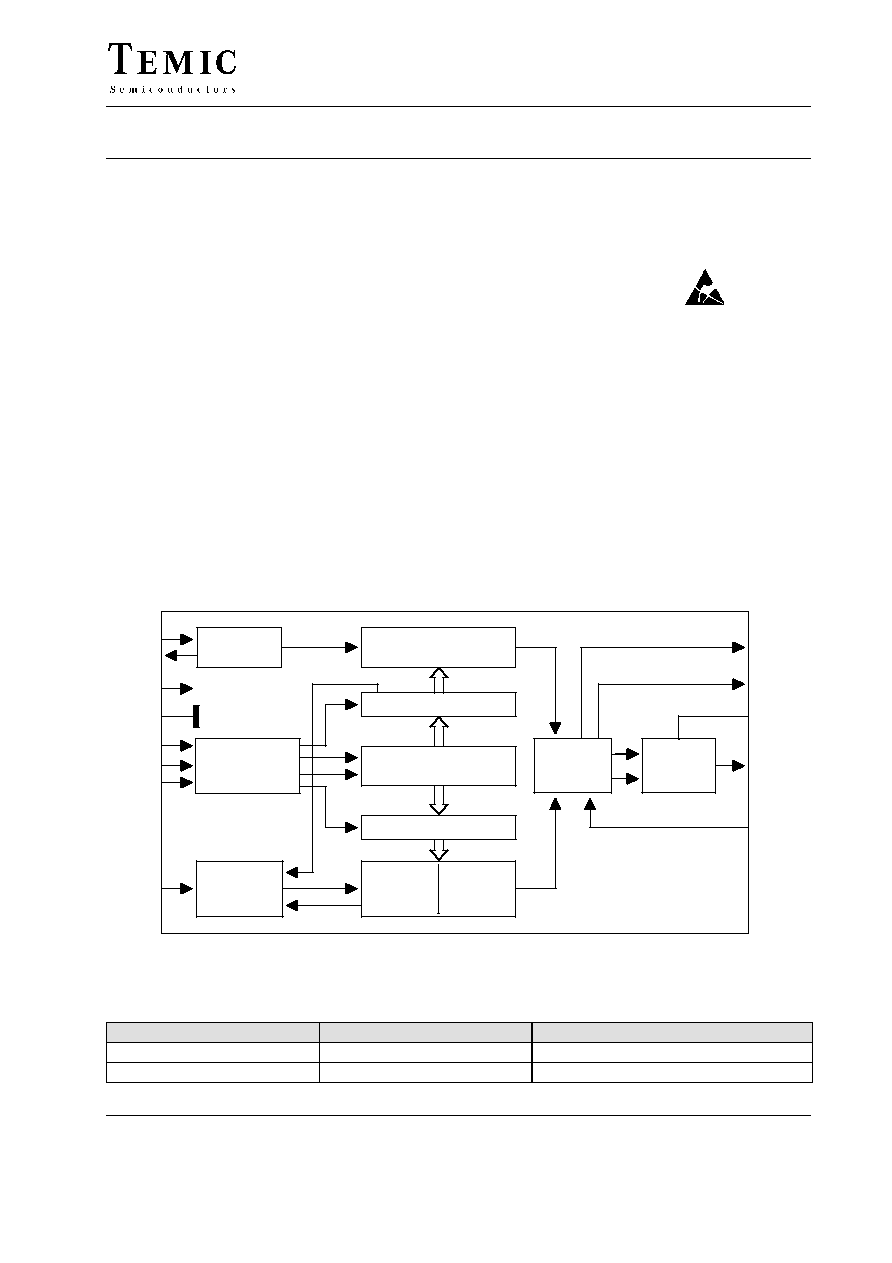
Block Diagram
Charge
pump
Prescaler
64/65
128/129
V
VS
18-bit
shift register
Phase
detector
Oscillator
14-bit
reference counter
Data
Clock
Osci
GND
1-bit latch
load control
PS
CP
LDo
Mo
RFi
Enable
7-bit
swallow
counter
15-bit latch
11-bit
main
18-bit latch
counter
SCP
Osco
17
3
15
1
8
11
7
4
10
6
14
13
5
93 7785 e
Figure 1. Block diagram
Ordering Information
Extended Type Number
Package
Remarks
U2781B-AFS
SS020
Rail, MOQ 830 pcs
U2781B-AFSG3
SS020
Tape and reel, MOQ 4000 pcs

U2781B
TELEFUNKEN Semiconductors
Rev. A3, 26-Nov-97
2 (10)
Functional Description
The IC is controlled by a 3-wire bus with Clock, Data and
Enable inputs for programming the scaling factors of the
programmable counter, the reference counter and the
prescaler.
A TCXO can be connected to the oscillator input (OSCi)
as an alternative solution to the common crystal reference
oscillator. In that case, the oscillator output (OSCo)
should be left open.
The charge pump-output operates as switched current
sources. The characteristics of the phase-locked loop can
be determinated by the external low-pass filter.
The phase characteristic of the phase detector is convert-
ible and thus matchable to different frequency/ tuning
voltage characteristics.
Pin Description
1
2
3
4
5
6
7
8
10
9
19
18
17
16
14
15
13
12
11
20
V
SCP
V
S
14775
CP
GND
LDo
NC
NC
Osco
Mo
NC
PS
Enable
Data
NC
NC
NC
RFi
Clock
Osci
NC
Figure 2. Pinning
Pin
Symbol
Function
¡¡¡
¡¡¡
1
¡¡¡¡¡
¡¡¡¡¡
Osci
¡¡¡¡¡¡¡¡¡¡
¡¡¡¡¡¡¡¡¡¡
Oscillator input
¡¡¡
¡¡¡
2
¡¡¡¡¡
¡¡¡¡¡
NC
¡¡¡¡¡¡¡¡¡¡
¡¡¡¡¡¡¡¡¡¡
Not connected
¡¡¡
¡¡¡
3
¡¡¡¡¡
¡¡¡¡¡
Osco
¡¡¡¡¡¡¡¡¡¡
¡¡¡¡¡¡¡¡¡¡
Oscillator output
¡¡¡
¡¡¡
4
¡¡¡¡¡
¡¡¡¡¡
V
SCP
¡¡¡¡¡¡¡¡¡¡
¡¡¡¡¡¡¡¡¡¡
Charge-pump supply voltage
¡¡¡
¡¡¡
5
¡¡¡¡¡
¡¡¡¡¡
V
s
¡¡¡¡¡¡¡¡¡¡
¡¡¡¡¡¡¡¡¡¡
Supply voltage
¡¡¡
¡¡¡
6
¡¡¡¡¡
¡¡¡¡¡
CP
¡¡¡¡¡¡¡¡¡¡
¡¡¡¡¡¡¡¡¡¡
Charge-pump output
¡¡¡
¡¡¡
7
¡¡¡¡¡
¡¡¡¡¡
GND
¡¡¡¡¡¡¡¡¡¡
¡¡¡¡¡¡¡¡¡¡
Ground
¡¡¡
¡¡¡
8
¡¡¡¡¡
¡¡¡¡¡
LDo
¡¡¡¡¡¡¡¡¡¡
¡¡¡¡¡¡¡¡¡¡
Lock-detector output
¡¡¡
¡¡¡
9
¡¡¡¡¡
¡¡¡¡¡
NC
¡¡¡¡¡¡¡¡¡¡
¡¡¡¡¡¡¡¡¡¡
Not connected
¡¡¡
¡¡¡
10
¡¡¡¡¡
¡¡¡¡¡
RFi
¡¡¡¡¡¡¡¡¡¡
¡¡¡¡¡¡¡¡¡¡
VCO input
¡¡¡
¡¡¡
11
¡¡¡¡¡
¡¡¡¡¡
Clock
¡¡¡¡¡¡¡¡¡¡
¡¡¡¡¡¡¡¡¡¡
3-wire bus Clock
¡¡¡
¡¡¡
12
¡¡¡¡¡
¡¡¡¡¡
NC
¡¡¡¡¡¡¡¡¡¡
¡¡¡¡¡¡¡¡¡¡
Not connected
¡¡¡
¡¡¡
13
¡¡¡¡¡
¡¡¡¡¡
Data
¡¡¡¡¡¡¡¡¡¡
¡¡¡¡¡¡¡¡¡¡
3-wire bus Data
¡¡¡
¡¡¡
14
¡¡¡¡¡
¡¡¡¡¡
Enable
¡¡¡¡¡¡¡¡¡¡
¡¡¡¡¡¡¡¡¡¡
3-wire bus Enable
¡¡¡
¡¡¡
15
¡¡¡¡¡
¡¡¡¡¡
PS
¡¡¡¡¡¡¡¡¡¡
¡¡¡¡¡¡¡¡¡¡
Phase select input
¡¡¡
¡¡¡
16
¡¡¡¡¡
¡¡¡¡¡
NC
¡¡¡¡¡¡¡¡¡¡
¡¡¡¡¡¡¡¡¡¡
Not connected
¡¡¡
¡¡¡
17
¡¡¡¡¡
¡¡¡¡¡
Mo
¡¡¡¡¡¡¡¡¡¡
¡¡¡¡¡¡¡¡¡¡
Monitor output for f
p
and f
r
¡¡¡
¡¡¡
18
¡¡¡¡¡
¡¡¡¡¡
NC
¡¡¡¡¡¡¡¡¡¡
¡¡¡¡¡¡¡¡¡¡
Not connected
¡¡¡
¡¡¡
19
¡¡¡¡¡
¡¡¡¡¡
NC
¡¡¡¡¡¡¡¡¡¡
¡¡¡¡¡¡¡¡¡¡
Not connected
¡¡¡
¡¡¡
20
¡¡¡¡¡
¡¡¡¡¡
NC
¡¡¡¡¡¡¡¡¡¡
¡¡¡¡¡¡¡¡¡¡
Not connected
Absolute Maximum Ratings
Parameters
Symbol
Value
Unit
¡¡¡¡¡¡¡¡¡¡¡¡¡¡¡¡¡
¡¡¡¡¡¡¡¡¡¡¡¡¡¡¡¡¡
Supply voltage
¡¡¡¡¡
¡¡¡¡¡
V
S
¡¡¡¡¡¡¡¡
¡¡¡¡¡¡¡¡
≠ 0.3 to 6
¡¡¡¡¡
¡¡¡¡¡
V
¡¡¡¡¡¡¡¡¡¡¡¡¡¡¡¡¡
¡¡¡¡¡¡¡¡¡¡¡¡¡¡¡¡¡
RF input
¡¡¡¡¡
¡¡¡¡¡
V
RF
¡¡¡¡¡¡¡¡
¡¡¡¡¡¡¡¡
V
S
¡¡¡¡¡
¡¡¡¡¡
V
¡¡¡¡¡¡¡¡¡¡¡¡¡¡¡¡¡
¡¡¡¡¡¡¡¡¡¡¡¡¡¡¡¡¡
Oscillator input voltage
¡¡¡¡¡
¡¡¡¡¡
V
Osci
¡¡¡¡¡¡¡¡
¡¡¡¡¡¡¡¡
1
¡¡¡¡¡
¡¡¡¡¡
V
¡¡¡¡¡¡¡¡¡¡¡¡¡¡¡¡¡
¡¡¡¡¡¡¡¡¡¡¡¡¡¡¡¡¡
Oscillator output voltage
¡¡¡¡¡
¡¡¡¡¡
V
Osco
¡¡¡¡¡¡¡¡
¡¡¡¡¡¡¡¡
1.5
¡¡¡¡¡
¡¡¡¡¡
V
¡¡¡¡¡¡¡¡¡¡¡¡¡¡¡¡¡
¡¡¡¡¡¡¡¡¡¡¡¡¡¡¡¡¡
Bus input voltage
¡¡¡¡¡
¡¡¡¡¡
V
BUS
¡¡¡¡¡¡¡¡
¡¡¡¡¡¡¡¡
6
¡¡¡¡¡
¡¡¡¡¡
V
¡¡¡¡¡¡¡¡¡¡¡¡¡¡¡¡¡
¡¡¡¡¡¡¡¡¡¡¡¡¡¡¡¡¡
Phase-select input voltage
¡¡¡¡¡
¡¡¡¡¡
V
PS
¡¡¡¡¡¡¡¡
¡¡¡¡¡¡¡¡
6
¡¡¡¡¡
¡¡¡¡¡
V
¡¡¡¡¡¡¡¡¡¡¡¡¡¡¡¡¡
¡¡¡¡¡¡¡¡¡¡¡¡¡¡¡¡¡
Charge-pump input voltage
¡¡¡¡¡
¡¡¡¡¡
V
SCP
¡¡¡¡¡¡¡¡
¡¡¡¡¡¡¡¡
6
¡¡¡¡¡
¡¡¡¡¡
V
¡¡¡¡¡¡¡¡¡¡¡¡¡¡¡¡¡
¡¡¡¡¡¡¡¡¡¡¡¡¡¡¡¡¡
Storage temperature
¡¡¡¡¡
¡¡¡¡¡
T
stg
¡¡¡¡¡¡¡¡
¡¡¡¡¡¡¡¡
≠ 40 to 125
¡¡¡¡¡
¡¡¡¡¡
∞
C
U2781B
TELEFUNKEN Semiconductors
Rev. A3, 26-Nov-97
3 (10)
Operating Range
Parameters
Symbol
Value
Unit
¡¡¡¡¡¡¡¡¡¡¡¡¡¡¡¡¡
¡¡¡¡¡¡¡¡¡¡¡¡¡¡¡¡¡
Supply voltage
¡¡¡¡¡
¡¡¡¡¡
V
S
¡¡¡¡¡¡¡¡
¡¡¡¡¡¡¡¡
2.7 to 5.5
¡¡¡¡¡
¡¡¡¡¡
V
¡¡¡¡¡¡¡¡¡¡¡¡¡¡¡¡¡
¡¡¡¡¡¡¡¡¡¡¡¡¡¡¡¡¡
Ambient temperature
¡¡¡¡¡
¡¡¡¡¡
T
amb
¡¡¡¡¡¡¡¡
¡¡¡¡¡¡¡¡
≠ 40 to 85
¡¡¡¡¡
¡¡¡¡¡
∞
C
Thermal Resistance
Parameters
Symbol
Value
Unit
¡¡¡¡¡¡¡¡¡¡¡¡¡¡¡¡¡
¡¡¡¡¡¡¡¡¡¡¡¡¡¡¡¡¡
Junction ambient
SSO20
¡¡¡¡¡
¡¡¡¡¡
R
thJA
¡¡¡¡¡¡¡¡
¡¡¡¡¡¡¡¡
140
¡¡¡¡¡
¡¡¡¡¡
K/W
Electrical Characteristics
T
amb
= 25
_C, V
S
= 2.7 to 5.5 V, unless otherwise specified
Parameters
Test Conditions / Pin
Symbol
Min
Typ
Max
Unit
¡¡¡¡¡¡¡¡¡¡¡¡¡¡¡¡¡¡¡¡¡¡¡¡¡¡¡¡¡¡¡¡
¡¡¡¡¡¡¡¡¡¡¡¡¡¡¡¡¡¡¡¡¡¡¡¡¡¡¡¡¡¡¡¡
DC supply
¡¡¡¡¡¡¡¡¡¡
¡¡¡¡¡¡¡¡¡¡
Supply voltage
¡¡¡¡¡¡¡¡
¡¡¡¡¡¡¡¡
¡¡¡¡
¡¡¡¡
V
s
¡¡¡¡
¡¡¡¡
2.7
¡¡¡¡
¡¡¡¡
¡¡¡¡
¡¡¡¡
5.5
¡¡¡¡
¡¡¡¡
V
¡¡¡¡¡¡¡¡¡¡
¡¡¡¡¡¡¡¡¡¡
Supply current
¡¡¡¡¡¡¡¡
¡¡¡¡¡¡¡¡
V
s
= 3 V
¡¡¡¡
¡¡¡¡
I
s
¡¡¡¡
¡¡¡¡
¡¡¡¡
¡¡¡¡
5
¡¡¡¡
¡¡¡¡
¡¡¡¡
¡¡¡¡
mA
¡¡¡¡¡¡¡¡¡¡
¡¡¡¡¡¡¡¡¡¡
Supply voltage CP
¡¡¡¡¡¡¡¡
¡¡¡¡¡¡¡¡
¡¡¡¡
¡¡¡¡
V
SCP
¡¡¡¡
¡¡¡¡
V
s
¡¡¡¡
¡¡¡¡
¡¡¡¡
¡¡¡¡
5.5
¡¡¡¡
¡¡¡¡
V
¡¡¡¡¡¡¡¡¡¡
¡¡¡¡¡¡¡¡¡¡
Supply current CP
¡¡¡¡¡¡¡¡
¡¡¡¡¡¡¡¡
V
CP
= 5 V, PLL in
locked condition
¡¡¡¡
¡¡¡¡
I
SCP
¡¡¡¡
¡¡¡¡
¡¡¡¡
¡¡¡¡
1
¡¡¡¡
¡¡¡¡
¡¡¡¡
¡¡¡¡
µ
A
¡¡¡¡¡¡¡¡¡¡¡¡¡¡¡¡¡¡¡¡¡¡¡¡¡¡¡¡¡¡¡¡
¡¡¡¡¡¡¡¡¡¡¡¡¡¡¡¡¡¡¡¡¡¡¡¡¡¡¡¡¡¡¡¡
RF input
¡¡¡¡¡¡¡¡¡¡
¡
¡¡¡¡¡¡¡¡
¡
¡¡¡¡¡¡¡¡¡¡
Input voltage
f
i
= 200 to 1100 MHz
¡¡¡¡¡¡¡¡
¡
¡¡¡¡¡¡
¡
¡¡¡¡¡¡¡¡
R
s
= 50
*)
R
s
= 50
*)
¡¡¡¡
¡
¡¡
¡
¡¡¡¡
V
imin
V
imax
¡¡¡¡
¡
¡¡
¡
¡¡¡¡
¡¡¡¡
¡
¡¡
¡
¡¡¡¡
20
200
¡¡¡¡
¡
¡¡
¡
¡¡¡¡
¡¡¡¡
¡
¡¡
¡
¡¡¡¡
mV
RMS
mV
RMS
¡¡¡¡¡¡¡¡¡¡
¡¡¡¡¡¡¡¡¡¡
Frequency range
¡¡¡¡¡¡¡¡
¡¡¡¡¡¡¡¡
¡¡¡¡
¡¡¡¡
f
imin
f
imax
¡¡¡¡
¡¡¡¡
1100
¡¡¡¡
¡¡¡¡
50
1250
¡¡¡¡
¡¡¡¡
¡¡¡¡
¡¡¡¡
MHz
MHz
¡¡¡¡¡¡¡¡¡¡
¡¡¡¡¡¡¡¡¡¡
Scaling factor prescaler
¡¡¡¡¡¡¡¡
¡¡¡¡¡¡¡¡
¡¡¡¡
¡¡¡¡
S
PSC
¡¡¡¡
¡¡¡¡
¡¡¡¡
¡¡¡¡
64/128
¡¡¡¡
¡¡¡¡
¡¡¡¡
¡¡¡¡
¡¡¡¡¡¡¡¡¡¡
¡¡¡¡¡¡¡¡¡¡
Scaling factors main counter
¡¡¡¡¡¡¡¡
¡¡¡¡¡¡¡¡
¡¡¡¡
¡¡¡¡
S
M
¡¡¡¡
¡¡¡¡
4
¡¡¡¡
¡¡¡¡
¡¡¡¡
¡¡¡¡
2047
¡¡¡¡
¡¡¡¡
¡¡¡¡¡¡¡¡¡¡
¡¡¡¡¡¡¡¡¡¡
Scaling factors swallow counter
¡¡¡¡¡¡¡¡
¡¡¡¡¡¡¡¡
¡¡¡¡
¡¡¡¡
S
S
¡¡¡¡
¡¡¡¡
0
¡¡¡¡
¡¡¡¡
¡¡¡¡
¡¡¡¡
127
¡¡¡¡
¡¡¡¡
¡¡¡¡¡¡¡¡¡¡¡¡¡¡¡¡¡¡¡¡¡¡¡¡¡¡¡¡¡¡¡¡
¡¡¡¡¡¡¡¡¡¡¡¡¡¡¡¡¡¡¡¡¡¡¡¡¡¡¡¡¡¡¡¡
Reference oscillator
¡¡¡¡¡¡¡¡¡¡
¡¡¡¡¡¡¡¡¡¡
Input voltage
¡¡¡¡¡¡¡¡
¡¡¡¡¡¡¡¡
R
s
= 50
*)
R
s
= 50
*)
¡¡¡¡
¡¡¡¡
V
imin
V
imax
¡¡¡¡
¡¡¡¡
¡¡¡¡
¡¡¡¡
20
200
¡¡¡¡
¡¡¡¡
¡¡¡¡
¡¡¡¡
mV
RMS
mV
RMS
¡¡¡¡¡¡¡¡¡¡
¡
¡¡¡¡¡¡¡¡
¡
¡¡¡¡¡¡¡¡¡¡
Frequency range
¡¡¡¡¡¡¡¡
¡
¡¡¡¡¡¡
¡
¡¡¡¡¡¡¡¡
¡¡¡¡
¡
¡¡
¡
¡¡¡¡
f
imin
f
imax
¡¡¡¡
¡
¡¡
¡
¡¡¡¡
¡¡¡¡
¡
¡¡
¡
¡¡¡¡
0,1
20
¡¡¡¡
¡
¡¡
¡
¡¡¡¡
¡¡¡¡
¡
¡¡
¡
¡¡¡¡
MHz
MHz
¡¡¡¡¡¡¡¡¡¡
¡¡¡¡¡¡¡¡¡¡
Scaling factor reference counter
¡¡¡¡¡¡¡¡
¡¡¡¡¡¡¡¡
¡¡¡¡
¡¡¡¡
S
R
¡¡¡¡
¡¡¡¡
4
¡¡¡¡
¡¡¡¡
¡¡¡¡
¡¡¡¡
16383
¡¡¡¡
¡¡¡¡
¡¡¡¡¡¡¡¡¡¡¡¡¡¡¡¡¡¡¡¡¡¡¡¡¡¡¡¡¡¡¡¡
¡¡¡¡¡¡¡¡¡¡¡¡¡¡¡¡¡¡¡¡¡¡¡¡¡¡¡¡¡¡¡¡
3-wire bus (Clock, Data, Enable) and PS
¡¡¡¡¡¡¡¡¡¡
¡¡¡¡¡¡¡¡¡¡
High input voltage
¡¡¡¡¡¡¡¡
¡¡¡¡¡¡¡¡
¡¡¡¡
¡¡¡¡
V
iH
¡¡¡¡
¡¡¡¡
1.5
¡¡¡¡
¡¡¡¡
0.9
¡¡¡¡
¡¡¡¡
¡¡¡¡
¡¡¡¡
V
¡¡¡¡¡¡¡¡¡¡
¡¡¡¡¡¡¡¡¡¡
Low input voltage
¡¡¡¡¡¡¡¡
¡¡¡¡¡¡¡¡
¡¡¡¡
¡¡¡¡
V
iL
¡¡¡¡
¡¡¡¡
0
¡¡¡¡
¡¡¡¡
¡¡¡¡
¡¡¡¡
0.4
¡¡¡¡
¡¡¡¡
V
¡¡¡¡¡¡¡¡¡¡
¡¡¡¡¡¡¡¡¡¡
High input current
¡¡¡¡¡¡¡¡
¡¡¡¡¡¡¡¡
¡¡¡¡
¡¡¡¡
I
iH
¡¡¡¡
¡¡¡¡
¡¡¡¡
¡¡¡¡
¡¡¡¡
¡¡¡¡
5
¡¡¡¡
¡¡¡¡
µ
A
¡¡¡¡¡¡¡¡¡¡
¡¡¡¡¡¡¡¡¡¡
Low input current
¡¡¡¡¡¡¡¡
¡¡¡¡¡¡¡¡
¡¡¡¡
¡¡¡¡
I
iL
¡¡¡¡
¡¡¡¡
≠5
¡¡¡¡
¡¡¡¡
¡¡¡¡
¡¡¡¡
¡¡¡¡
¡¡¡¡
µ
A
¡¡¡¡¡¡¡¡¡¡¡¡¡¡¡¡¡¡¡¡¡¡¡¡¡¡¡¡¡¡¡¡
¡¡¡¡¡¡¡¡¡¡¡¡¡¡¡¡¡¡¡¡¡¡¡¡¡¡¡¡¡¡¡¡
Monitor output (Emitter follower)
¡¡¡¡¡¡¡¡¡¡
¡¡¡¡¡¡¡¡¡¡
High output voltage
¡¡¡¡¡¡¡¡
¡¡¡¡¡¡¡¡
V
s
= 3 V
¡¡¡¡
¡¡¡¡
V
iH
¡¡¡¡
¡¡¡¡
2.1
¡¡¡¡
¡¡¡¡
2.2
¡¡¡¡
¡¡¡¡
¡¡¡¡
¡¡¡¡
V
¡¡¡¡¡¡¡¡¡¡
¡¡¡¡¡¡¡¡¡¡
Low output voltage
¡¡¡¡¡¡¡¡
¡¡¡¡¡¡¡¡
I
MO
= 0.5 mA
¡¡¡¡
¡¡¡¡
V
iL
¡¡¡¡
¡¡¡¡
¡¡¡¡
¡¡¡¡
1.8
¡¡¡¡
¡¡¡¡
1.9
¡¡¡¡
¡¡¡¡
V
¡¡¡¡¡¡¡¡¡¡
¡¡¡¡¡¡¡¡¡¡
Charge-pump output
¡¡¡¡¡¡¡¡
¡¡¡¡¡¡¡¡
¡¡¡¡
¡¡¡¡
¡¡¡¡
¡¡¡¡
¡¡¡¡
¡¡¡¡
¡¡¡¡
¡¡¡¡
¡¡¡¡
¡¡¡¡
¡¡¡¡¡¡¡¡¡¡
¡¡¡¡¡¡¡¡¡¡
Source current
¡¡¡¡¡¡¡¡
¡¡¡¡¡¡¡¡
V
CP
= 5 V
¡¡¡¡
¡¡¡¡
I
source
¡¡¡¡
¡¡¡¡
¡¡¡¡
¡¡¡¡
≠1
¡¡¡¡
¡¡¡¡
¡¡¡¡
¡¡¡¡
mA
¡¡¡¡¡¡¡¡¡¡
¡¡¡¡¡¡¡¡¡¡
Sink current
¡¡¡¡¡¡¡¡
¡¡¡¡¡¡¡¡
¡¡¡¡
¡¡¡¡
I
sink
¡¡¡¡
¡¡¡¡
¡¡¡¡
¡¡¡¡
1
¡¡¡¡
¡¡¡¡
¡¡¡¡
¡¡¡¡
mA
¡¡¡¡¡¡¡¡¡¡
¡¡¡¡¡¡¡¡¡¡
Leakage current
¡¡¡¡¡¡¡¡
¡¡¡¡¡¡¡¡
V
CP
= 5 V
¡¡¡¡
¡¡¡¡
I
leak
¡¡¡¡
¡¡¡¡
¡¡¡¡
¡¡¡¡
±
5
¡¡¡¡
¡¡¡¡
¡¡¡¡
¡¡¡¡
nA
¡¡¡¡¡¡¡¡¡¡¡¡¡¡¡¡¡¡¡¡¡¡¡¡¡¡¡¡¡¡¡¡
¡¡¡¡¡¡¡¡¡¡¡¡¡¡¡¡¡¡¡¡¡¡¡¡¡¡¡¡¡¡¡¡
Lock-detektor output (open collector)
¡¡¡¡¡¡¡¡¡¡
¡¡¡¡¡¡¡¡¡¡
Saturation voltage
¡¡¡¡¡¡¡¡
¡¡¡¡¡¡¡¡
I
LD
= 1 mA
¡¡¡¡
¡¡¡¡
V
sat
¡¡¡¡
¡¡¡¡
¡¡¡¡
¡¡¡¡
0.2
¡¡¡¡
¡¡¡¡
0.4
¡¡¡¡
¡¡¡¡
V
¡¡¡¡¡¡¡¡¡¡
¡¡¡¡¡¡¡¡¡¡
Leakage current
¡¡¡¡¡¡¡¡
¡¡¡¡¡¡¡¡
V
LD
= 5 V
¡¡¡¡
¡¡¡¡
I
leak
¡¡¡¡
¡¡¡¡
¡¡¡¡
¡¡¡¡
5
¡¡¡¡
¡¡¡¡
¡¡¡¡
¡¡¡¡
nA
*) RMS voltage at 50
W
U2781B
TELEFUNKEN Semiconductors
Rev. A3, 26-Nov-97
4 (10)
Functional Description
The reference- and the programmable counter can be
programmed by the 3-wire bus (Clock, Data and Enable).
The Data Signal is transfered bit by bit into the shift
register during the rising edge, starting with the MSB-bit.
As soon as the enable signal is in high condition, the
content of the shift register will be taken over either into
the 15-bit reference counter latch (C = H) or into the
18-bit latch of the programmable counter (C = L)
Reference Counter (15bit shift register)
¡¡¡
¡¡¡
LSB
¡¡¡
¡¡¡
¡¡¡
¡¡¡
¡¡¡
¡¡¡
¡¡
¡¡
¡¡¡
¡¡¡
¡¡¡
¡¡¡
¡¡¡
¡¡¡
¡¡¡
¡¡¡
¡¡¡
¡¡¡
¡¡¡
¡¡¡
¡¡¡
¡¡¡
¡¡¡
¡¡¡
¡¡¡
¡¡¡
¡¡
¡¡
¡¡¡¡
¡¡¡¡
MSB
¡¡¡
¡¡¡
C
¡¡¡
¡¡¡
R0
¡¡¡
¡¡¡
R1
¡¡¡
¡¡¡
R2
¡¡
¡¡
R3
¡¡¡
¡¡¡
R4
¡¡¡
¡¡¡
R5
¡¡¡
¡¡¡
R6
¡¡¡
¡¡¡
R7
¡¡¡
¡¡¡
R8
¡¡¡
¡¡¡
R9
¡¡¡
¡¡¡
R10
¡¡¡
¡¡¡
R11
¡¡¡
¡¡¡
R12
¡¡
¡¡
R13
¡¡¡¡
¡¡¡¡
PSC
C:
Control bit High
PSC: Prescaler scaling factor bit: High ≠ 64/65
Low ≠ 128/129
S
PSC
= 64 or 128
R0 to R13:
These bits are setting the reference counter S
R
S
R
= R0
2
0
+ R1
2
1
+ to + R12
2
12
+ R13
2
13
permitted scaling factors for S
R
: 4 to 16383
Programmable Counter (18-bit shift register)
¡¡¡
¡¡¡
LSB
¡¡¡
¡¡¡
¡¡
¡¡
¡¡¡
¡¡¡
¡¡
¡¡
¡¡¡
¡¡¡
¡¡
¡¡
¡¡¡
¡¡¡
¡¡¡
¡¡¡
¡¡
¡¡
¡¡¡
¡¡¡
¡¡
¡¡
¡¡¡
¡¡¡
¡¡
¡¡
¡¡¡
¡¡¡
¡¡
¡¡
¡¡¡
¡¡¡
¡¡
¡¡
¡¡¡¡
¡¡¡¡
MSB
¡¡¡
¡¡¡
C
¡¡¡
¡¡¡
S0
¡¡
¡¡
S1
¡¡¡
¡¡¡
S2
¡¡
¡¡
S3
¡¡¡
¡¡¡
S4
¡¡
¡¡
S5
¡¡¡
¡¡¡
S6
¡¡¡
¡¡¡
M0
¡¡
¡¡
M1
¡¡¡
¡¡¡
M2
¡¡
¡¡
M3
¡¡¡
¡¡¡
M4
¡¡
¡¡
M5
¡¡¡
¡¡¡
M6
¡¡
¡¡
M7
¡¡¡
¡¡¡
M8
¡¡
¡¡
M9
¡¡¡¡
¡¡¡¡
M10
C:
Control bit Low
S0 to S6:
These bits are setting the swallow counter S
S
.
S
S
= S0
2
0
+ S1
2
1
+ to + S5
2
5
+ S6
2
6
permitted scaling factors for S
S
: 0 to 127, S
S
< S
M
M0 to M10 : These bits are setting the main counter S
M
.
S
M
= M0
2
0
+ M1
2
1
+ to + M9
2
9
+ M10
2
10
permitted scaling factors for S
M
: 4 to 2047
Total scaling factor S
P
of the programmable counter
S
P
= (S
PSC
S
M
) + S
S
Condition: S
S
< S
M
VCO Frequency
f
VCO
= ((S
PSC
S
M
) + S
S
)
f
RefOsc
/ S
R

U2781B
TELEFUNKEN Semiconductors
Rev. A3, 26-Nov-97
5 (10)
Timing 3-Wire Bus
C = 1 : Reference scaler date
93 7787 e
MSB
LSB
C = 0 : Prog. scaler data
R 0
P 0
R 6
P 8
R 7
P 9
R 13
P 16
PSC
P 17
Enable
Clock
Data
t
5
t
1
t
2
t
3
t
4
All times t
1
to t
5
> 1
ms
Figure 3.
Phase-Detector Polarity
The polarity of the phase detector can be changed with the
PS input. Depending on the PS input level, the charge-
pump current will also be inverted. The monitor output
signal MO (emitter follower output with ECL level) will
be switched over from f
P
to f
R
simultanously.
PS = High or Open
PS = Low
¡¡¡¡¡¡
¡
¡¡¡¡
¡
¡¡¡¡¡¡¡
¡
¡¡¡¡¡
¡
CP
¡¡¡¡¡¡¡
¡
¡¡¡¡¡
¡
MO
¡¡¡¡¡¡
¡¡¡¡¡
¡
CP
¡¡¡¡¡¡¡
¡
¡¡¡¡¡
¡
MO
¡¡¡¡¡¡
¡¡¡¡¡¡
f
R
> f
P
¡¡¡¡¡¡¡
¡¡¡¡¡¡¡
I
sink
¡¡¡¡¡¡¡
¡¡¡¡¡¡¡
f
R
¡¡¡¡¡¡
¡¡¡¡¡¡
I
source
¡¡¡¡¡¡¡
¡¡¡¡¡¡¡
f
P
¡¡¡¡¡¡
¡¡¡¡¡¡
f
R
< f
P
¡¡¡¡¡¡¡
¡¡¡¡¡¡¡
I
source
¡¡¡¡¡¡¡
¡¡¡¡¡¡¡
f
R
¡¡¡¡¡¡
¡¡¡¡¡¡
I
sink
¡¡¡¡¡¡¡
¡¡¡¡¡¡¡
f
P
¡¡¡¡¡¡
¡¡¡¡¡¡
f
R
= f
P
¡¡¡¡¡¡¡
¡¡¡¡¡¡¡
0
¡¡¡¡¡¡¡
¡¡¡¡¡¡¡
f
R
¡¡¡¡¡¡
¡¡¡¡¡¡
0
¡¡¡¡¡¡¡
¡¡¡¡¡¡¡
f
P
Depending on the VCO frequency versus tuning voltage characteristic, the PS input has to be programmed as follows:
For increasing tuning voltage and increasing frequency:
PS = High or open
decreasing frequency:
PS = Low.