
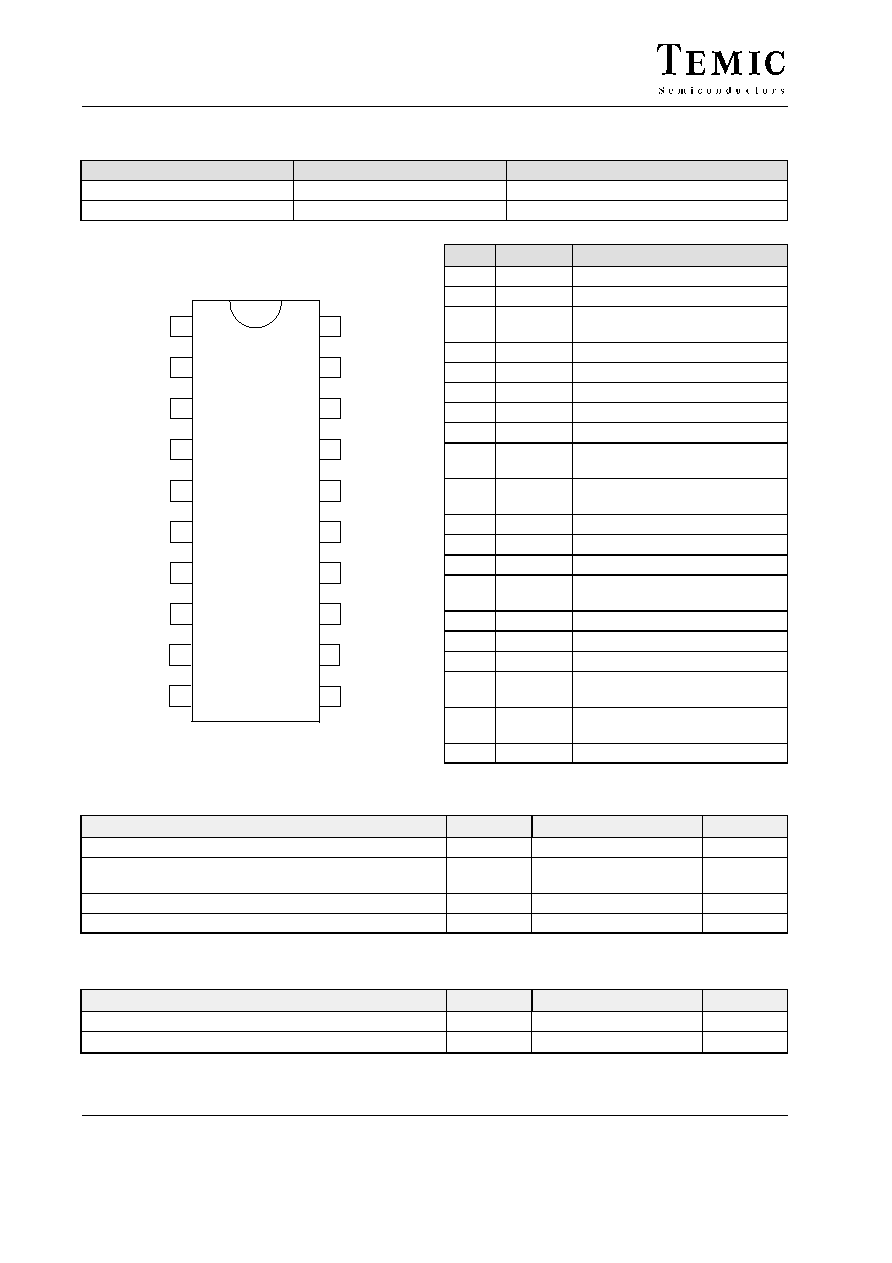
U2782B
TELEFUNKEN Semiconductors
Rev. A4, 17-Oct-97
1 (10)
1100 MHz Twin PLL
Description
The IC U2782B is a low power twin PLL manufactured
with TEMIC's advanced UHF process. The maximum
operating frequency is 1100 MHz for both PLLs.
It features a wide supply voltage range from 2.7 to 5.5 V.
Prescaler 64/65 and power down function for both PLL's
is integrated. Applications are CT1, IS54, JDC etc.
Electrostatic sensitive device.
Observe precautions for handling.
Features
D Very low current consumption (typical 3 V/11 mA)
D Supply voltage range 2.7 to 5.5 V
D Maximum input frequency: 1100 for both PLLs
D 2 pins for separate power down functions
D Output for PLL lock status
D Prescaler 64/65 for both inputs
D SSO20 package
D ESD protected according to MIL-STD 833
method 3015 cl.2
Benefits
D Low current consumption leads to extended talk time
D Twin PLL saves costs and space
D One foot print for all TEMIC twin PLL's saves design-
in time
Block Diagram
12 bit reference divider 2
12 bit latch 2
17 bit latch 2
17 bit main divider 2
17 bit
Shift register
17 bit latch 1
17 bit main divider 1
12 bit reference divider 1
12 bit latch 1
16 bit latch
Control functions
Oscillator
on / off
divide by 2
64 / 65 Prescaler 1
64 / 65 Prescaler 2
3 bit
Load control
Phase
detector 1
Phase
detector 2
Charge
pump 1
Charge
pump 2
Pump
bias
Lock
select
Ports
Power
down
Test
9
14
1
20
5I/Port 0
HPD1/Port1
HPD2/Port4
Port3
Lock Port2
10
3
17
CP1
V
Scp
19
18
Iset
CP2
7
8
4
2
6
15
V
S
analog
V
S
digital
DGND
AGND
OSCi
OSCo
5
RFi1
11
12
13
16
Clock
Data
Enable
RFi2
94 8916
Figure 1.
U2782B
TELEFUNKEN Semiconductors
Rev. A4, 17-Oct-97
2 (10)
Ordering Information
Extended Type Number
Package
Remarks
U2782B-AFS
SSO20
Rail, MOQ 830 PCS
U2782B-AFSG3
SSO20
Tape and Reel, MOQ 4000 pcs
Pin Description
1
2
3
4
5
6
7
8
10
9
19
18
17
16
14
15
13
12
11
20 Port 3
Iset
CP 2
V
Scp
RFi 2
GND
A
HPD2/Port 4
Enable
Data
Clock
5I/Port 0
V
S
digital
CP 1
V
S
analog
RFi 1
GND
D
OSC
i
OSC
o
HPD1/Port 1
Lock/Port 2
95 9622
Pin
Symbol
Function
1
5I/Port 0
5I � Control input / o.c.output
2
V
S
digital
Power supply digital section
3
CP 1
Charge pump output of
synthesizer 1
4
V
S
analog Power supply analog section
5
RFi 1
RF divider input synthesizer
6
GND
D
Ground for digital section
7
OSC
i
Reference oscillator input
8
OSC
o
Reference oscillator output
9
HPD 1/
Port 1
Hardware power down input of
synthesizer 1 / o.c.output
10
Lock/
Port 2
Lock output / o.c.output /
testmode output
11
Clock
3-wire-bus: serial clock input
12
Data
3-wire-bus: serial data input
13
Enable
3-wire-bus: serial enable input
14
HPD 2/
Port 4
Hardware power down input of
synthesizer 2 / o.c.output
15
GND
A
Ground for analog section
16
RFi 2
RF divider input synthesizer 2
17
V
Scp
Charge pump supply voltage
18
CP 2
Charge pump output of
synthesizer 2
19
Iset
Reference pin for charge pump
currents
20
Port 3
o.c.output
Absolute Maximum Ratings
Parameters
Symbol
Value
Unit
Supply voltage
Pins 2, 4 and 17
V
S
, V
Scp
6
V
Input voltage
Pins 1, 3, 5, 8, 9, 10, 11, 12, 13,
14, 15, 16, 18 and 20
V
i
0 to V
S
V
Junction temperature
T
j
125
�
C
Storage temperature range
T
stg
� 40 to + 125
�
C
Operating Range
Parameters
Symbol
Value
Unit
Supply voltage
Pins 2, 4 and 17
V
S
, V
Scp
2.7 to 5.5
V
Ambient temperature range
T
amb
� 40 to + 85
�
C

U2782B
TELEFUNKEN Semiconductors
Rev. A4, 17-Oct-97
3 (10)
Thermal Resistance
Parameters
Symbol
Value
Unit
Junction ambient
SSO20
R
thja
140
K/W
Electrical Characteristics
T
amb
= 25
_C, V
S
= 2.7 to 5.5 V, V
Scp
= 5 V, unless otherwise specified
Parameters
Test conditions
Symbol
Min.
Typ.
Max.
Unit
��������������������������������
��������������������������������
DC Supply
���������
���������
Supply current
���������
���������
V
S
= 3V, SPD1 = SPD2 = 0
����
����
I
S
����
����
0.5
����
����
0.8
����
����
1.1
����
����
mA
���������
���������
Supply current
���������
���������
V
S
= 3V, SPD1 = SPD2 = 1
����
����
I
S
����
����
7
����
����
11
����
����
13
����
����
mA
���������
�
�������
�
���������
Supply current CP
���������
�
�������
�
���������
V
CP
= 5 V, PLL in lock
condition
����
�
��
�
����
I
CP
����
�
��
�
����
0
����
�
��
�
����
1
����
�
��
�
����
10
����
�
��
�
����
�
A
PLL 1 + PLL2
Input voltage
f
RFi1
= 200 � 1100 MHz
V
RFi1
20
200
mV
RMS
Scaling factor prescaler
S
PSC
64/65
Scaling factor main
counter
S
M
5
2047
Scaling factor swallow
counter
S
S
0
63
Reference counter
S
R
5
4096
Reference oscillator
Recommended crystal
series resistance
10
200
W
External reference input
frequency
AC coupled sinewave
RF/2 = 0
RF/2 = 1
OSC
i
1
1
20
40
MHz
External reference input
amplitude
AC coupled sinewave
2)
OSC
i
100
mV
RMS
Logic input levels (Clock, Data, Enable, HPD1, HPD2, 5I)
High input level
V
iH
1.5
V
Low input level
V
iL
0
0.4
V
High input current
I
iH
�5
5
mA
Low input current
I
iL
�5
5
mA
Logic output levels (Port 0, 1, 2, 3, 4, Lock)
Leakage current
V
OH
= 5.5 V
I
L
10
mA
Saturation voltage
I
OL
= 0.5 mA
V
SL
0.4
V
Charge pump output (R
set
= tbd.)
Source current
V
CP
x
V
Scp
/2
PLL2
5I = L
PLL1
5I = H
PLL1
I
source
� 1
�0.2
�1
mA
Sink current
V
CP
x
V
Scp
/2
PLL2
5I = L
PLL1
5I = H
PLL1
I
sink
1
0.2
1
mA
Leakage current
V
CP
x
V
Scp
/2
I
L
"5
nA
1)
RMS voltage at 50
W;
2)
OSC
o
is open if an external reference frequency is applied
U2782B
TELEFUNKEN Semiconductors
Rev. A4, 17-Oct-97
4 (10)
Serial Bus Programming
Reference and programmable counters can be
programmed by the 3-wire-bus (Clock, Data and Enable).
After setting enable signal to high condition, the data sta-
tus is transfered but by but on the rising edge of the clock
signal into the shift register, starting with the MSB-bit.
After the Enable signal returns to low condition the
programmed information is loaded according to the
addressbits (last three bits) into the addressed latch.
Additional leading bits are ignored and there is no check
made how many clock pulses arrived during enable high
condition. In powerdown mode the 3-wire-bus remains
active and the IC can be programmed.
Data is entered with the most significant bit first. The
leading bits deliver the divider or control information.
The trailing three bits are the address field. There are six
different addresses used. The trailing address bits are
decoded upon the falling edge of the Enable signal. The
internal Loadpulse is beginning with the falling edge of
the Enable signal and ending with falling edge of the
Clock signal. Therefore a minimum holdtime clock-
enable t
HCE
is required.
Bit Allocation
MSB
LSB
Bit
1
Bit
2
Bit
3
Bit
4
Bit
5
Bit
6
Bit
7
Bit
8
Bit
9
Bit
10
Bit
11
Bit
12
Bit
13
Bit
14
Bit
15
Bit
16
Bit
17
Bit
18
Bit
19
Bit
20
data bits
address bits
D16 D15 D14 D13 D12
D11
D10
D9
D8
D7
D6
D5
D4
D3
D2
D1
D0
A2
A1
A0
PLL1
M10
M9
M8
M7
M6
M5
M4
M3
M2
M1
M0
S5
S4
S3
S2
S1
PLL1
S0
0
0
1
PLL1
R11
R10
R9
R8
R7
R6
R5
R4
R3
R2
R1
PL1
R0
0
1
0
PLL2
M10
M9
M8
M7
M6
M5
M4
M3
M2
M1
M0
S5
S4
S3
S2
S1
PLL2
S0
0
1
1
PLL2
R11
R10
R9
R8
R7
R6
R5
R4
R3
R2
R1
PLL2
R0
1
0
0
RF/
2
Test
5IP
TRI
2
TRI
1
PS2
PS1
H2P H1P
LP
B
LPA
P4
P3
P2
P1
P0
1
0
1
SP
D 5I
SP
D 2
SP
D 1
1
1
0
Scaling Factors
S0 ... S5:
These bits are setting the swallow counter S
S
.
T
S
= S0*2
0
+ S1*2
1
+ ... + S4*2
4
+ S5*2
5
allowed scalling factors for S
S
: 0 ... 63, T
S
< T
M
M0 ... M10: These bits are setting the main counter S
M
.
T
M
= M0*2
0
+ M1*2
1
+ ... + M9*2
9
+ M10*2
10
allowed scalling factors for S
M
: 5 ... 2047
S
PGD
: Total scalling factor of the programmable counter:
S
PGD
= (64*S
M
) + S
S
Condition: S
S
< S
M
R0 ... R11:
These bits are setting the reference counter S
R
.
S
R
= R0*2
0
+ ... + R10*2
10
+ R11*2
11
allowed scalling factors for S
R
: 5 ... 4096
S
RFD
: Total scalling factor of the reference counter:
RF/2 = 1:
S
RFD
= 2 * S
R
RF/2 = 0:
S
RFD
= S
R

U2782B
TELEFUNKEN Semiconductors
Rev. A4, 17-Oct-97
5 (10)
Serial Programming Bus
Control Bits:
P0 ... P4:
o.c. output ports (1 = high impedance)
LPA, LPB:
selection of P2 output or locksignal
LPA
LPB
function of pin 10
0
0
o.c. output P2
0
1
locksignal of synthesizer 2
1
0
locksignal of synthesizer 1
1
1
wiredor locksignal of both synthesizer
H1P, H2P:
selection of P1/4 output or hardware power down input of synthesizer 1/2 (0 = Port / 1 = HPD)
5IP:
selection of P0 output or high current switching input for the charge pump current of synthesizer 1
(0 = Port / 1 = charge pump 1 current switch input)
PS1, PS2:
phase selection of synthesizer 1 and synthesizer 2 (1 = normal / 0 = invers)
PS-PLL1/2 = 1
PS-PLL1/2 = 0
CP1/2
CP1/2
f
R
> f
P
I
sink
I
source
f
R
< f
P
I
source
I
sink
f
R
= f
P
0
0
RF/2: divide by 2 prescaler for reference divider (0 = off / 1 = on)
SPD1, SPD2: software power down bit of synthesizer 1/2 (0 = powerdown / 1 = powerup)
5I:
software switch for the charge pump current of synthesizer 1 (0 = low current / 1 = high current)
TRI1, TRI2: enables tristate for the charge pump of synthesizer 1/2 (0 = normal / 1 = tristate)
TEST: enables counter testmode (0 = disabled / 1 = enabled)
TEST
LPA
LPB
PS1
PS2
Testsignal
at pin 10
1
1
0
1
x
RFD1
1
1
0
0
x
PGD1
1
0
1
x
1
RFD2
1
0
1
x
0
PGD2
To operate the software power down mode the following condition must be set: HXP = 0; power up and power down
will be set by SPDX = 1 (on) and SPDX = 0 (off).
To operate the hardware power down mode the following condition must be set: HXP = 1; SPDX = 1; power up and
power down will be set by high and low state at the hardware power down pins 9/14.
High current of charge pump synthesizer 1 is active when 5I = 1 and if 5IP = 1 the charge pump current control input
pin 1 is in high state.