 | –≠–ª–µ–∫—Ç—Ä–æ–Ω–Ω—ã–π –∫–æ–º–ø–æ–Ω–µ–Ω—Ç: U2791B | –°–∫–∞—á–∞—Ç—å:  PDF PDF  ZIP ZIP |
TELEFUNKEN Semiconductors
U2791B
Rev. A2: 08.06.1995
1 (11)
1000 MHz Quadrature Demodulator
Description
U2791B silicon monolithic integrated circuit is a
quadrature demodulator that is manufactured using
TELEFUNKEN's advanced UHF technology. This
demodulator features a frequency range from
100 ≠ 1000 MHz, low current consumption, selectable
gain, power down mode and is adjustment free. The IC is
suitable for direct conversion and image rejection
applications in digital radio systems up to 1 GHz such as
cellular radio, cordless telephone, cable TV and satellite
TV systems.
Features
D Supply voltage 5 V (typ.)
D Very low power consumption 125 mW (typ.)
D Very good image rejection by means of phase control
loop for precise 90
∞
phase shifting
D Duty cycle regeneration for single ended LO input
signal
D Low LO input level ≠10 dBm (typ.)
D LO ≠ frequency from 100 MHz to 1 GHz
D Power down mode
D 25 dB gain control
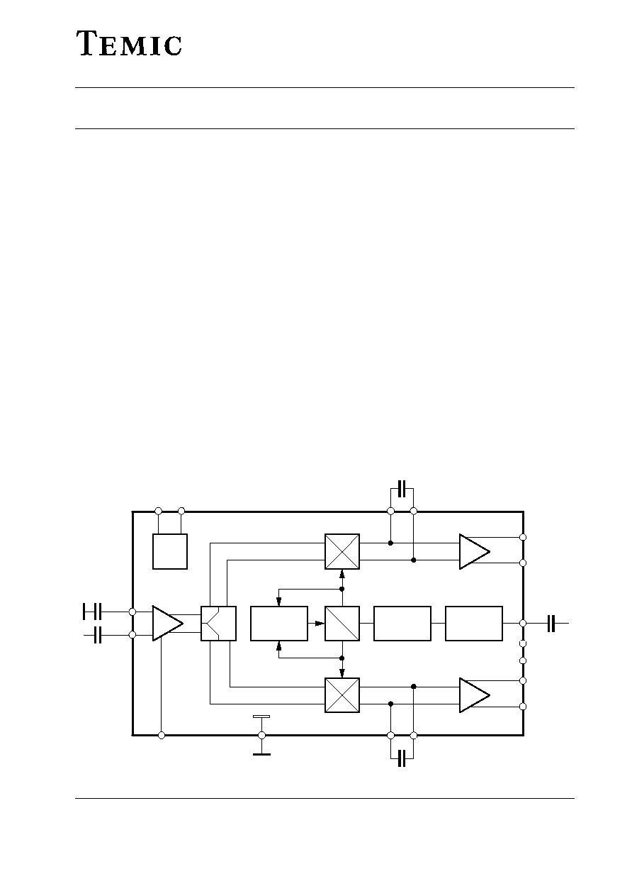
Block Diagram
90
∞
Control
loop
90
∞
0
∞
Frequency
doubler
Duty cycle
regenerator
Power
down
14
5,6
V
S
PD
4
3
17
1
2
19
20
10
9
15,16,18
11
GC
GND
7
8
RFin
IIX
II
OUTPUT
IX
I
LO
12
13
PC
PCX
OUTPUT
QX
Q
QQ
QQX
95 9755
TELEFUNKEN Semiconductors
U2791B
Rev. A2: 08.06.1995
2 (11)
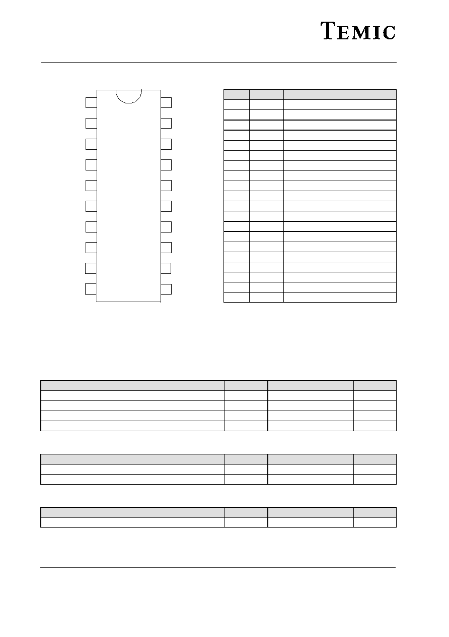
Pin Description
1
2
3
4
5
6
7
8
10
9
19
18
17
16
14
15
13
12
11
20
IX
I
II
V
S
V
S
QQ
QQX
IIX
QX
Q
GND
LO
in
GND
GND
PD
PC
PCX
GC
94 9441
RFX
in
RF
in
Pin
Symbol
Function
1
IX
IX output
2
I
I output
3
II
II low pass filter I
4
IIX
IIX low pass filter I
5
V
S
Supply voltage
6
V
S
Supply voltage
7
RF
in
RF input
8
RFX
in
RFX input
9
QQ
QQ low pass filter Q
10
QQX
QQX low pass filter Q
11
GC
GC gain control
12
PCX
PCX phase control
13
PC
PC phase control
14
PD
PD power down
15
GND
Ground
16
GND
Ground
17
LO
in
LO input
18
GND
Ground
19
Q
Q output
20
QX
QX output
Electrostatic sensitive device observe precautions for handling.
Absolute Maximum Ratings
Parameters
Symbol
Value
Unit
Supply voltage
Pins 5 and 6
V
S
6
V
Input voltage
Pins 7, 8 and 17
V
i
0 to V
S
V
Junction temperature
T
j
125
∞
C
Storage temperature range
T
stg
≠40 to 125
∞
C
Operating Range
Parameters
Symbol
Value
Unit
Supply voltage range
Pins 5 and 6
V
S
4.75 to 5.25
V
Ambient temperature range
T
amb
≠40 to 85
∞
C
Thermal Resistance
Parameters
Symbol
Value
Unit
Junction ambient
SSO 20
R
thJA
140
K/W

TELEFUNKEN Semiconductors
U2791B
Rev. A2: 08.06.1995
3 (11)
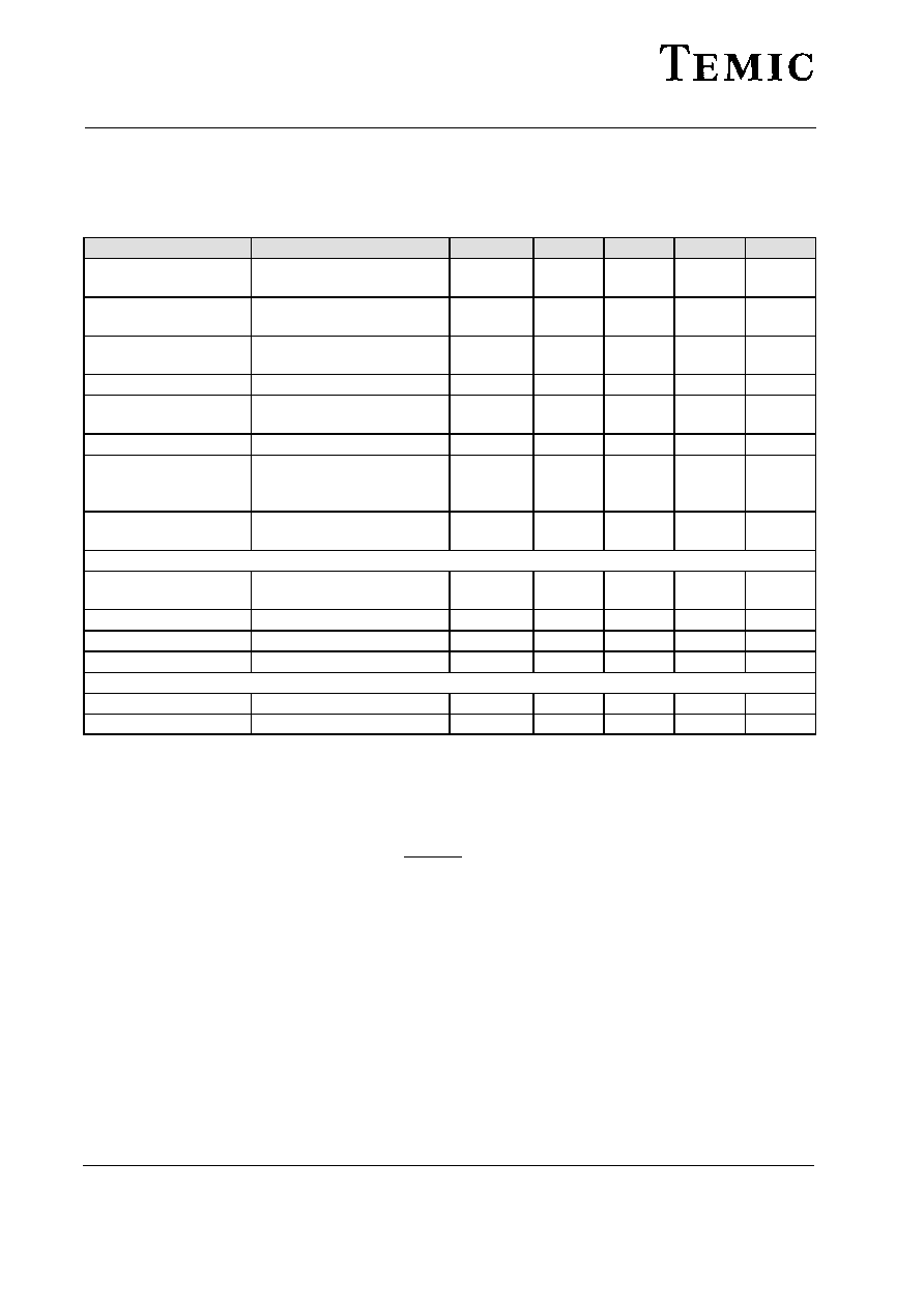
Electrical Characteristics
Test conditions (unless otherwise specified); V
S
= 5 V, T
amb
= 25
∞
C, referred to test circuit
System impedance Z
O
= 50
W, fiLO = 950 MHz, PiLO = ≠10 dBm
Parameters
Test Conditions / Pins
Symbol
Min.
Typ.
Max.
Unit
Supply voltage range
Pins 5 and 6
V
S
4.75
5.25
V
Supply current
Pins 5 and 6
I
S
30
mA
Power down mode, PD
"OFF "mode supply
current
V
PD
0.5 V Pins 5, 6 V
PD
= 1.0 V
Pin 14
Note 1
IsPD
1
20
mA
Switch voltage
Pin 14
"Power ON"
VPON
4
V
"Power DOWN"
VPOFF
1
V
LO input, LO
in
Pin 17
Frequency range
fiLO
100
1000
MHz
Input level
Note 2
PiLO
≠12
≠10
≠5
dBm
Input impedance
See figure 6
ZiLO
50
W
Voltage standing wave
ratio
See figure 2
VSWRLO
1.2
2
Duty cycle range
LODCR
0.4
0.6
RF input, RF
in
Noise figure (DSB)
symmetrical output
@ 950 MHz Note 3
@ 100 MHz Pins 7 and 8
NF
12
10
dB
Frequency range
Pins 7 and 8
fiRF
>fiLO
≠1 dB input
compression point
Pins 7 and 8
High gain
Low gain
ICPHG
ICPLG
≠8
+3.5
dBm
Second order IIP
Note 4
Pins 7 and 8
IIP2HG
35
dBm
Third order IIP
Pins 7 and 8
High gain
Low gain
IIP3HG
IIP3LG
+3
+13
dBm
LO leakage
Pins 7 and 8
Symmetric input
Asymmetric input
LOL
≠60
≠55
dBm
Input impedance
Pins 7 and 8
see figure 6
ZiRF
500
W¯
0.8pF
Note 1: During power down status a load circuitry with dc-isolation to GND is assumed otherwise a current of
I
(V
S
≠0.8 V) /RI has to be added to the above power down current for each output I, IX, Q, QX.
Note 2: The required LO-Level is a function of the LO-frequency (see figure 3).
Note 3: Measured with input matching. For 950 MHz the optional transmission line T3 at the RF input may be used
for this purpose. Noise figure measurements without using the differential output signal result in a worse noise
figure.
Note 4: Using Pins 7 and 8 as a symmetric RF input, the second order IIP can be improved.
TELEFUNKEN Semiconductors
U2791B
Rev. A2: 08.06.1995
4 (11)
Electrical Characteristics
Test conditions (unless otherwise specified); V
S
= 5 V, T
amb
= 25
∞
C, referred to test circuit
System impedance Z
O
= 50
W, fiLO = 950 MHz, PiLO = ≠10 dBm
Parameters
Test Conditions / Pins
Symbol
Min.
Typ.
Max.
Unit
I/O outputs
Emitter follower
I = 0.6 mA
I, IX / Q,
QX
3-dB bandwidth
w/o external C
Note 5
Pins 1, 2, 19 and 20
BWI/Q
30
MHz
I/Q amplitude
imbalance
Pins 1, 2, 19 and 20
AII/Q
±
0.2
dB
I/Q quadrature error
Pins 1, 2, 19 and 20
QEI/Q
±
1.5
Deg
I/Q maximum output
swing
Pins 1, 2, 19 and 20
Symm. output R
L
> 5 k
W
Max I/Q
2
V
PP
DC output voltage
Pins 1, 2, 19 and 20
VOUT
2.8
V
DC output offset voltage Note 6 Pins 1, 2, 19 and 20
VOFSI/Q
I/IX
Q/QX
30
mV
Output impedance
Pins 1, 2, 19 and 20
see figure 6
Zout
50
W
Gain control, GC
Control range power
gain, gain high/gain low
Note 7
Pin 11
GCR
PGH/GGL
25
23/≠2
dB
Switch voltage
"Gain high"
Pin 11
GCVHigh
1
V
"Gain low"
Note 8
Pin 11
GCVLow
V
Settling time, ST
Power "OFF " ≠ "ON "
STON
< 4
ms
Power "ON " ≠ "OFF "
STOFF
< 4
ms
Note 5: Due to test board parasitics this bandwidth is reduced and not equal for I, IX, Q, QX.
If symmetry and full bandwidth is required the low-pass Pins 3, 4, 9 and 10 should be isolated from the board.
The bandwidth of the I/Q outputs can be increased further by using a resistor between the Pins 3, 4, 9 and 10.
This resistors shunt the internal loads of RI
5.4 kW The decrease in gain here has to be considered.
Note 6: Output emitter follower internal acurrent I = 0.6 mA allows only small voltage swing with a 50
W load.
For low signal distortion the load impedance should be RI
5 k
W.
Note 7: Referred to the level of the output vector I
2
) Q
2
.
Note 8: The low gain status is achieved with an open or high ohmic Pin 11. A recommended application circuit for
switching between high and low gain status is shown in figure 1.

TELEFUNKEN Semiconductors
U2791B
Rev. A2: 08.06.1995
5 (11)
Test Circuit
95 9841
*
optional for single ended tests (notice 3 dB bandwidth of AD620)
T1, T2 = transmission line Z
O
= 50
W.
If no GC function is required, connect Pin 11 to GND.
For high and low gain status GC' is to be switched to GND respectively to V
S
.
Figure 1.