 | –≠–ª–µ–∫—Ç—Ä–æ–Ω–Ω—ã–π –∫–æ–º–ø–æ–Ω–µ–Ω—Ç: U2795B | –°–∫–∞—á–∞—Ç—å:  PDF PDF  ZIP ZIP |
TELEFUNKEN Semiconductors
U2795B
Rev. A2: 08.06.1995
1 (13)
2.5-GHz Double Balanced Mixer
Description
U2795B is a 2.5-GHz mixer for WLAN and RF telecom-
munications equipment, e.g., DECT and PCN, built with
TELEFUNKEN's advanced bipolar technology. A
double balanced approach was chosen to assure good
isolation characteristics and a minimum of spurious
products. The input and output are single ended, and their
characteristics are programmable. No output transformer
or balun is required.
Features
D Supply voltage range: 2.7 to 5.5 V
D Single-ended output, no balun required
D Single-ended input for RF and LO
D Exellent isolation characteristics
D Power down mode
D IP3 and compression point programmable
D 2.5-GHz operating frequency
D SO-8 package
Benefits
D Reduced system costs due to few external component
(no balun) requirements
D Standard independent product
D 3-V operation reduces the battery count and saves
space
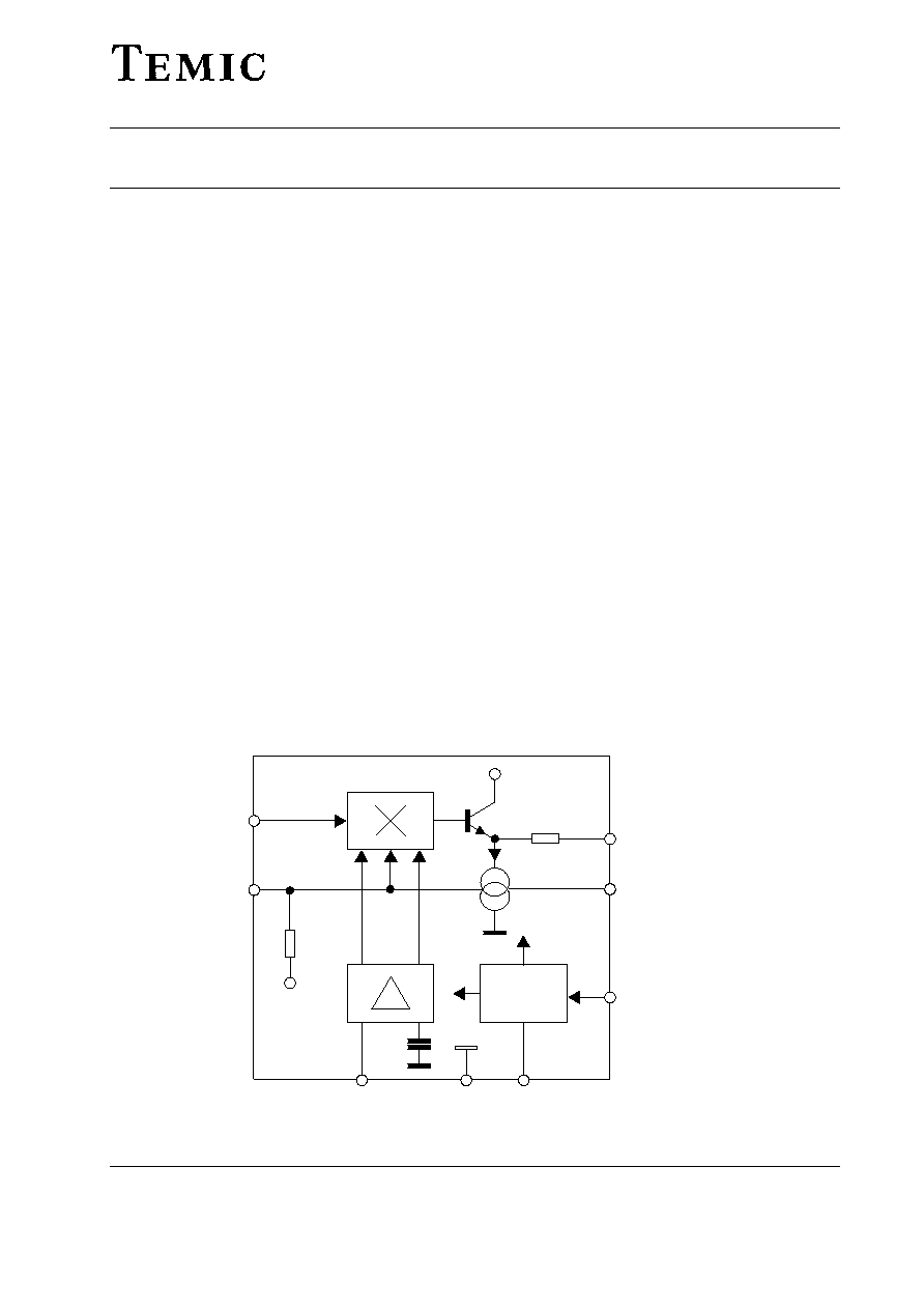
Block Diagram
R1
Voltage
regulator
VH
R
V
VS
2
RF
3
P
VH
7
LO
6
GND
VS 1
4
8
R2
5
IF
PD
93 7811 e
i
i
S
o
o

TELEFUNKEN Semiconductors
U2795B
Rev. A2: 08.06.1995
2 (13)
Pin Description
1
2
3
4
5
6
7
8
V
S
RF
I
P
S
O
IF
O
LO
i
PD
94 7890 e
GND
Pin
Symbol
Function
1
V
S
Supply voltage
2
RF
i
RF input
3
P
Progamming port IP3, CP
4
S
O
Output symmetry
5
IF
O
IF output
6
GND
Ground
7
LO
i
LO input
8
PD
Power down
Functional Description
Supply Voltage
The IC is designed for a supply voltage of 2.7 to 5.5 V. As
the IC is internally stabilized, the performance of the
circuit is nearly independent of the supply voltage.
Input Impedance
Input impedance, Z
RFi
, is about 700
W with an additional
capacitive component. This condition provides the best
noise figure in combination with a matching network.
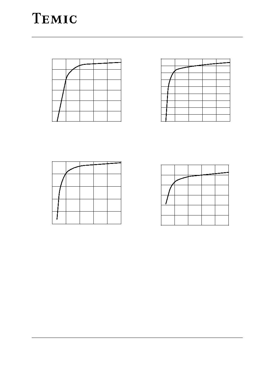
3. Order Intercept Point (IP3)
Voltage divider, R
P
/ R
1,
determinates both the input and
output intercept point, IIP3 and OIP3. If R
P
is infinity the
IIP3 has the maximum of about ≠ 4 dBm.
The IP3/R
P
characteristics are shown in figure 1 and 2.
Output Impedance and Intercept Point
Output impedance is shown in figure 9.
Both low output impedance and a high intercept point are
with reference to a high value of R
P
.
Current Consumption, I
S
Depending on the chosen input and output conditions of
the IC, the current consumption, I
S,
is between 4 mA and
10 mA. The current consumption in dependence of Rp is
shown in figure 4.
Power Down
This feature provides an extension of battery life. If this
function is not used, Pin 8 has to be connected to V
S
(Pin 1).
Output Symmetry
The symmetry of the load current can be matched and so
be optimized for a given load impedance.

TELEFUNKEN Semiconductors
U2795B
Rev. A2: 08.06.1995
3 (13)
Absolute Maximum Ratings
Parameters
Symbol
Value
Unit
Supply voltage
Pin 1
V
S
6
V
Input voltage
Pins 2, 3, 7 and 8
V
I
0 to V
S
V
Junction temperature
T
j
125
∞
C
Storage temperature range
T
stg
≠ 40 to + 125
∞
C
Thermal Resistance
Parameters
Symbol
Value
Unit
Junction ambient
SO 8
R
thja
175
K/W
Operating Range
Parameters
Symbol
Value
Unit
Supply voltage range
Pin 1
V
S
2.7 to 5.5
V
Ambient temperature range
T
amb
≠ 40 to + 85
∞
C

TELEFUNKEN Semiconductors
U2795B
Rev. A2: 08.06.1995
4 (13)
Electrical Characteristics
V
S
= 3 V, f
LOi
= 1 GHz, IF = 900 MHz, RF = 100 MHz, R
P
=
R, system impedance Zo = 50 W, T
amb
= 25
∞C, R
T
= 56
W
reference point Pin 6, unless otherwise specified
Parameters
Test Conditions / Pin
Symbol
Min.
Typ.
Max.
Unit
Supply voltage range
Pin 1
V
S
2.7
5.5
V
Typical supply current
range
1
Pin 1
I
S
4
11
mA
Maximum supply current
Pin 1
I
S
13
mA
Conversion power gain
R
L
= 50
W, R
T
=
R
R
L
= 50
W, R
T
= 56
W
PG
C
PG
C
9
4
dB
dB
Operating frequencies
RF
i
frequency
Pin 2
RF
i
10
2500
MHz
LO
i
frequency
Pin 7
f
LOi
50
2500
MHz
IF
o
frequency
Pin 5
f
IFo
50
2500
MHz
Isolation
LO spurious at R
Fi
Pin 7 to 2
P
iLO
= ≠10 to 0 dBm
IS
LO-RF
≠ 30
dBm
RF
i
to LO
i
Pin 2 to 7
P
iRF
= ≠25 dBm
IS
RF-LO
35
dB
LO spurious at IF
o
Pin 7 to 5,
P
iLO
= ≠ 10 to 0 dBm
IS
LO-IF
≠ 25
dBm
IF
o
to LO
i
Pin 5 to 7
IS
IF-LO
30
dB
Output (IF)
Output compression point
Pin 5
CP
o
≠ 10
dBm
Input (RF)
Input impedance
Pin 2
Z
RFi
700
Wk0.8pF
W
Input compression point
Pin 2
CP
i
≠ 14
dBm
Third order input
intercept point
Pin 2
IIP3
≠ 4
dBm
Input (LO)
LO level
Pin 7
P
iLO
≠ 6
dBm
Voltage standing wave ratio (VSWR)
Input LO
Pin 7
VSWR
LOi
< 2
Output IF
Pin 4
VSWR
IFo
< 2
Noise performance
Noise figure
P
iLO
= 0 dBm, R
T
=
R
NF
10
dB
Power down mode
Supply current
Pin 1 V
PD
< 0.5 V
Pin 1 V
PD
= 0 V
I
SPD
< 5
30
mA
Power down voltage
"Power ON"
Pin 8 V
S
= 3.5 to 5.5 V
V
S
= 2.7 to 3.5 V
V
PON
V
S
≠ 0.5
V
S
V
S
+ 0.5
V
S
+ 0.5
V
V
"Power DOWN"
Pin 8
V
PDN
1
V
Power down current
Pin 8 Power ON
Power DOWN
I
PON
I
PDN
0.15
< 5
mA
mA
Settling time
Pin 8 to 5
t
sPD
< 30
ms
Note 1:
Depending on R
P
TELEFUNKEN Semiconductors
U2795B
Rev. A2: 08.06.1995
5 (13)
0
20
40
60
80
≠10
≠9
≠8
≠7
≠6
≠4
IIP3 ( dBm )
R
p
( k
W )
100
94 9235
≠5
Figure 1. IIP3 versus resistor Rp, IF: 900 MHz
0
20
40
60
80
≠25
≠20
≠15
≠10
≠5
0
OIP3 ( dBm )
R
p
( k
W )
100
94 9236
Figure 2. OIP3 versus resistor Rp, IF: 900 MHz
0
20
40
60
80
≠13
≠9
≠5
≠1
3
Gain ( dB )
R
p
( k
W )
100
94 9237
Figure 3. Gain versus resistor Rp, LO: 1030 MHz,
level ≠10 dBm; RF: 130 MHz, ≠30 dBm, R
T
= 56
W
0
20
40
60
80
0
2
4
6
8
12
I ( mA
)
s
R
p
( k
W )
100
94 9238
10
Figure 4. Supply current I
S
versus resistor Rp