
U2796B
Preliminary Information
Rev. A2, 15-Oct-98
1 (11)
2-GHz Single Balanced Mixer
Description
The U2796B-FP is a 2-GHz down conversion mixer for
telecommunication systems, e.g. cellular radio, CT1,
CT2, DECT, PCN, using TEMIC Semiconductors
advanced bipolar technology. The U2796B is well suited
for the receiver portion of the RF circuit. Single balanced
structure has been chosen for the best noise performance
and low current consumption. The IIP3 is programmable.
Features
D Supply voltage range: 2.7 to 5.5 V
D Exellent isolation characteristics
D Low current consumption: 3.2 mA without R
IP3
D IIP3 programmable
D Input frequency operating range up to 2 GHz
D RF characteristic nearly independent of
supply voltage
Benefits
D Stand alone product
D Low current consumption extends talk time
D 3-V operation requires small space for batteries
Block Diagram
Duty cycle
control loop
Buffer
Mixer
Voltage
regulator
E
BP
2
3
RF
5
4
IF
S
V
6,8
7 LO
1
93 7758 e
i
C
i
O
IFO
B
Figure 1.
U2796B
Preliminary Information
Rev. A2, 15-Oct-98
3 (11)
Electrical Characteristics
Test conditions (unless otherwise specified):
V
S
= 3 V, f
LO
= 900 MHz; I
M
= 1.2 mA, T
amb
= 25
∞
C. System impedance Z
O
= 50
Parameters
Test conditions / Pin
Symbol
Min.
Typ.
Max.
Unit
Supply voltage
Pin 1
V
S
2.7
5.5
V
Supply current
R
IP3
=
R, Pin
1
I
S
2.8
3.2
3.7
mA
Conversion power gain
RL = 3 k
, R
IP3
=
R
f
LO
= 900 MHz
PG
C
9
dB
Figure 4
f
LO
= 1700 MHz
f
IF
= 45 MHz
9
Isolation
LO-spurious at RF
in
Pi
LO
= ≠10 dBm
Figure 5
Pin 7 to 2
IS
LORF
≠ 35
dBm
RF to LO
Pi
RF
= ≠25 dBm Pin 2 to 7
f
LO
= 900 MHz
IS
RFLO
30
40
dB
Figure 6
f
LO
= 1700 MHz
20
Operating frequencies
RF frequency
Pin 2
RF
i
2000
MHz
LO
in
frequency
Pin 7
LO
i
2000
MHz
IF
out
frequency
Pins 4 and 5
IF
o
300
MHz
Input level
RF input (≠ 1 dB comp.)
RL = 50
, Pin
2
Pi
RF
≠ 15
dBm
3rd order intercept
point
Pi
LO
= ≠10 dBm, R
IP3
=
R
Figure 2
Pin 2
IIP3
≠4
dBm
LO input
Pin 7
P
iLO
≠ 6
0
dBm
Impedances
RF input
Pin 2
Z
iRF
25
LO input
Pin 7
Zi
LO
50
IF output
Pins 4 and 5
Z
oIF
u10 k
//
0.9 pF
Noise figure (DSB)
Pi
LO
= 0dBm, RL
u 3 k
f
LO
= 900 MHz
NF
50
9
dB
Figure 7
f
LO
= 1700 MHz
12
Voltage standing wave
ratio LO
Pin 7
VSWR-
LO
1.3
2
Note: I
M
= Internal mixer current (see figure 2)
U2796B
Rev. A2, 15-Oct-98
Preliminary Information
4 (11)
0
400
800
1200
1600
1.0
1.5
2.0
2.5
3.0
3.5
I ( mA
)
M
RE (
W )
2000
93 7825 e
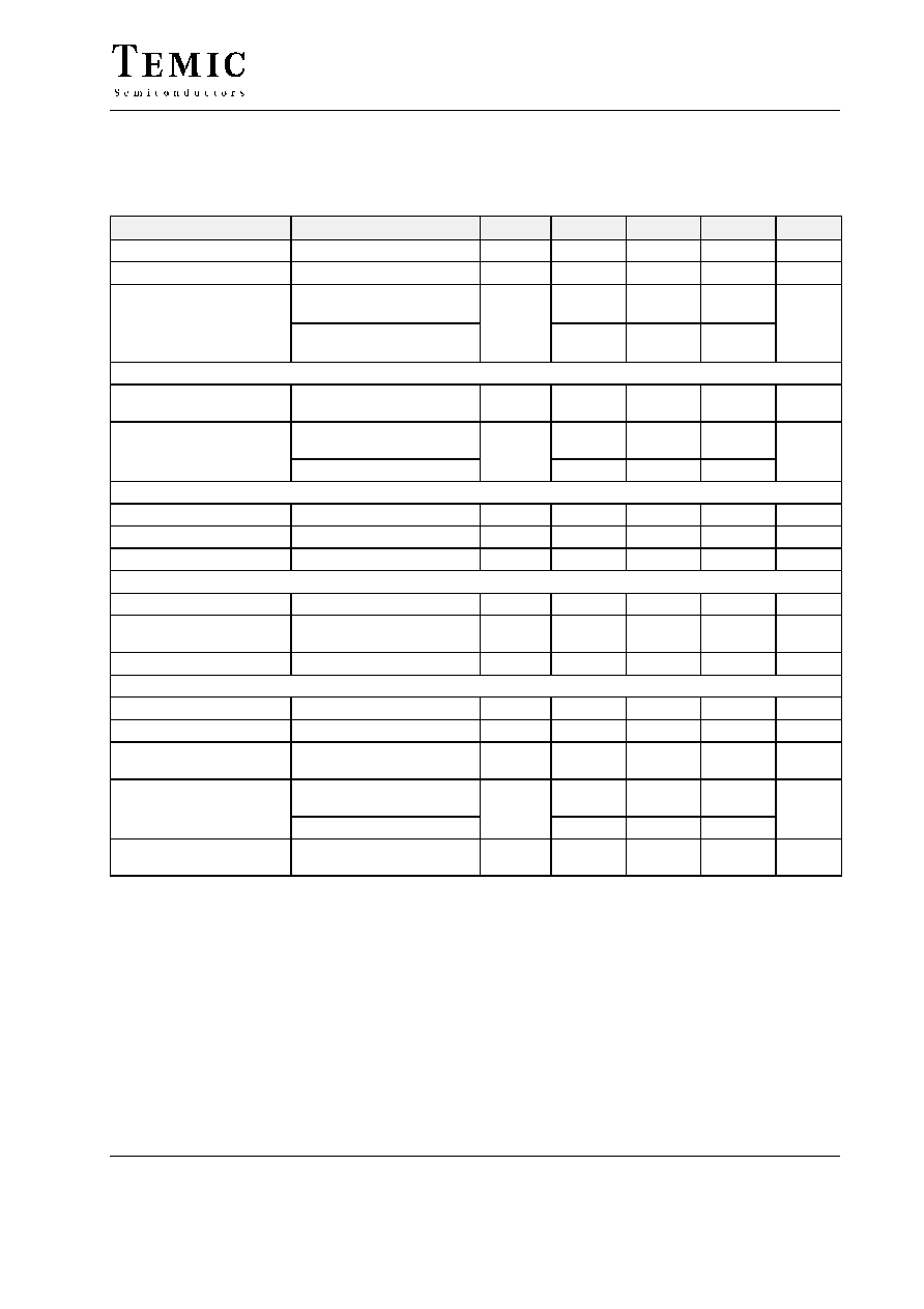
Figure 3. Mixer current (I
M
) versus RE
1
2
≠7
≠4
≠1
2
5
8
IIP3 ( dBm )
I
M
( mA )
3
93 7827 e
Figure 4. Third-order input intercept IIP3 point versus I
M
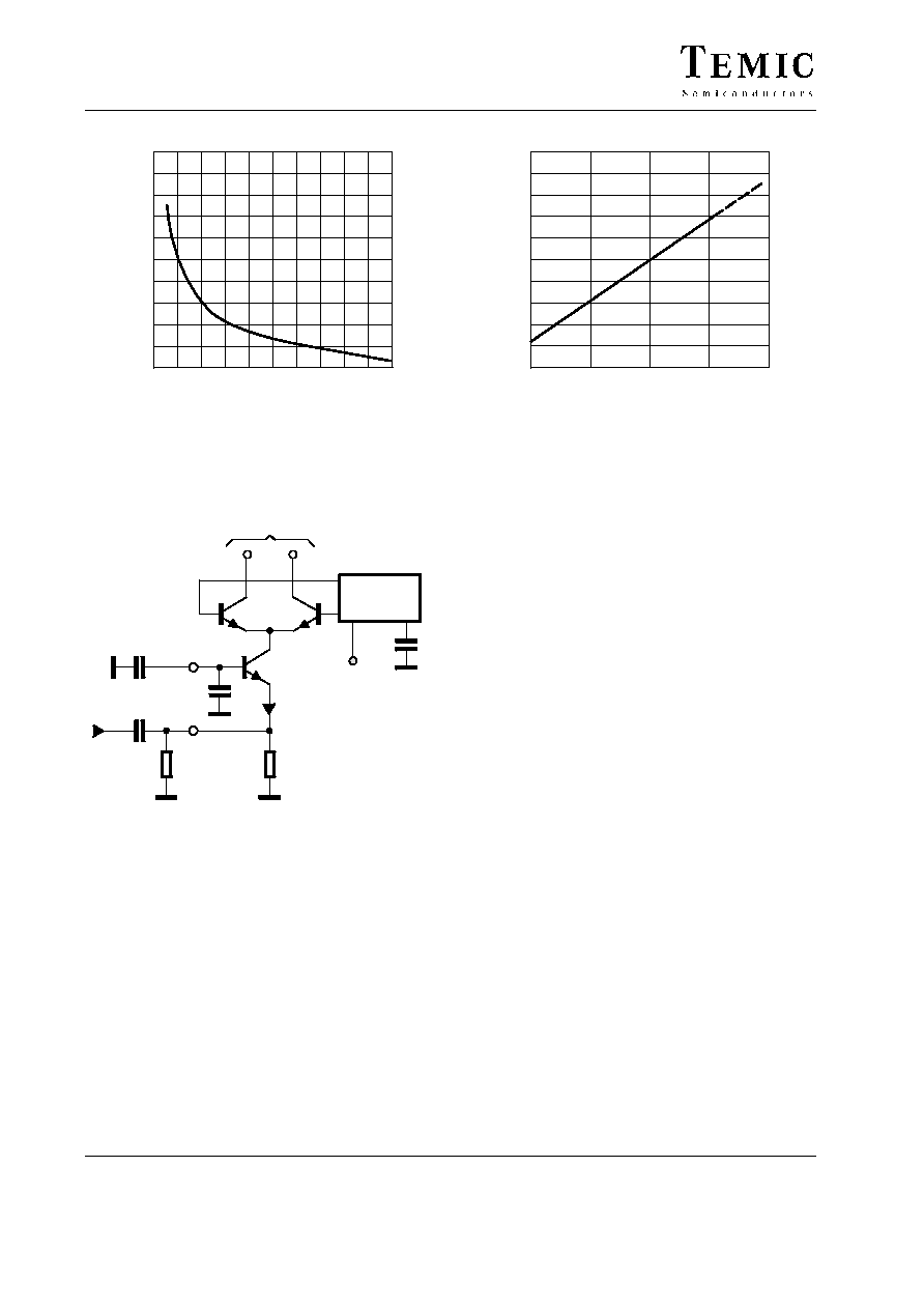
LO buffer
LO
7
3
2
E
R
IF
5
4
RF
M
I
93 7759 e
i
O
i
Figure 5. Mixer circuitry

