 | –≠–ª–µ–∫—Ç—Ä–æ–Ω–Ω—ã–π –∫–æ–º–ø–æ–Ω–µ–Ω—Ç: U2861B-M | –°–∫–∞—á–∞—Ç—å:  PDF PDF  ZIP ZIP |
U2861B
Preliminary Information
TELEFUNKEN Semiconductors
Rev. A1, 20-May-97
1 (11)
Mono FM Sound Demodulator for TV Systems
Description
The U2861B is an alignment-free FM sound IF demo-
dulator for all TV standards from 4.5 MHz up to 6.5 MHz
(standard M, N, B/G, I, D/K). The circuit includes two
switchable audio inputs and volume control. With a
supply voltage of 5 V, the U2861B is suitable for TV,
VCR and Multimedia applications.
Features
D Completely alignment-free
D PLL demodulator for FM intercarrier sound IF signals
(mono)
D Two audio switches
D Very few external components
D Volume control by DC voltage
D Supply voltage: 5 V; low power consumption
5 k
W
VCO
3
Bandgap
reference
6
7
10
12
1
AF1
in
V
S
8
AF2
out
14
13
2
4
Decoupling
De-
emphasis
9
11
Volume
control
Sound IF
input
96 11832
5
FM
mute
Audio
switch1
Audio
switch2
AF1
out
AF2
in
Switch2
Switch1
v
i,AF1
C
dec
v
i,SIF
GND
C
ref
V
S
C
dem
V
SW1
v
o,AF1
V
SW2
v
i,AF2
V
vol
v
o,AF2
V
mute
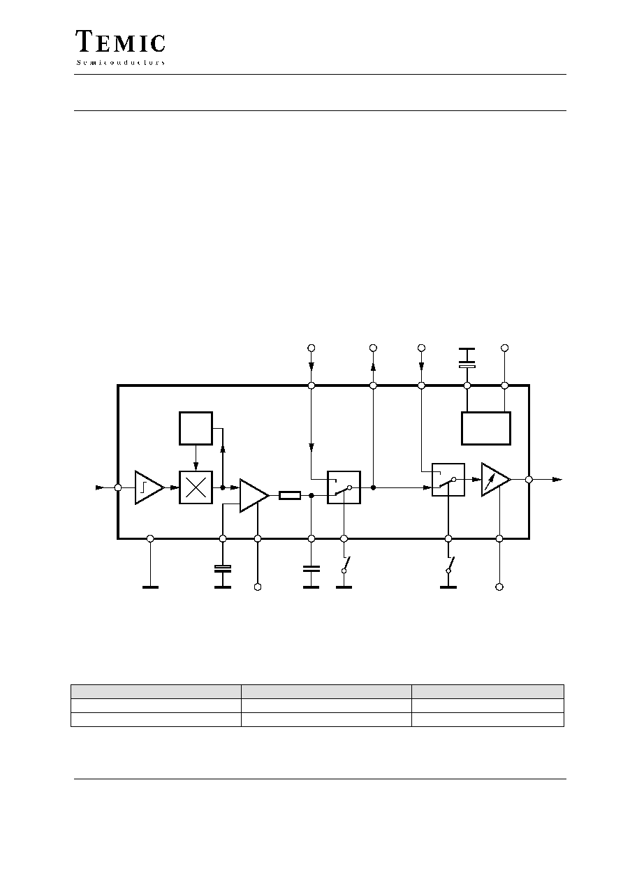
Figure 1. Block diagram
Ordering Information
Extended Type Number
Package
Remarks
¡¡¡¡¡¡¡¡¡¡¡
¡¡¡¡¡¡¡¡¡¡¡
U2861B ≠ M
¡¡¡¡¡¡¡¡¡¡¡¡
¡¡¡¡¡¡¡¡¡¡¡¡
DIP14
¡¡¡¡¡¡¡¡¡¡¡
¡¡¡¡¡¡¡¡¡¡¡
¡¡¡¡¡¡¡¡¡¡¡
¡¡¡¡¡¡¡¡¡¡¡
U2861B ≠ MFPG3
¡¡¡¡¡¡¡¡¡¡¡¡
¡¡¡¡¡¡¡¡¡¡¡¡
SO14
¡¡¡¡¡¡¡¡¡¡¡
¡¡¡¡¡¡¡¡¡¡¡
taped on reel
U2861B
TELEFUNKEN Semiconductors
Rev. A1, 20-May-97
Preliminary Information
2 (11)
Circuit Description
Sound IF Limiter Amplifier
The intercarrier signal coming from the sound filter is fed
to a 7-stage limiter amplifier. This guarantees high input
sensitivity and excellent AM suppression.
PLL ≠ FM Demodulator
The alignment-free "Phase-Locked-Loop" (PLL) FM
demodulator covers a wide frequency range of 4.5 MHz
up to 6.5 MHz with excellent noise performance. Due to
the fact that the voltage-to-frequency characteristic is
linear, a low harmonic distortion can be achieved. The
free-running frequency of the internal VCO circuit is
about 5.5 MHz.
The demodulated FM signal is led via de-emphasis and
buffered to Pin 12. The de-emphasis low pass filter con-
sists of an internal 5-k
W series resistor and an external
capacitor at Pin 14. The FM muting is possible by switch-
ing Pin 5 to ground.
Audio Switch 1
The first audio switch (Pin 13) has inputs for the demodu-
lated FM signal and the external AF1 signal from Pin 1.
For multistandard purposes, it is possible to handle inter-
nal FM and external AM audio signals. The output of
switch1 is also permanently available at Pin 12 (e. g. for
SCART interface).
Audio Switch 2 and Volume Control
The second audio switch (Pin 11) has inputs for the audio
signal from switch 1 and the external AF2 signal at Pin 10.
The switched AF signal is fed to volume control. The out-
put voltage can be controlled by a DC voltage at Pin 9.
Internal Voltage Stabilizer
The internal bandgap reference ensures constant perfor-
mance independent of supply voltage and temperature.
Pin Description
Pin
Symbol
Function
¡¡¡
¡¡¡
1
¡¡¡¡¡
¡¡¡¡¡
v
i,AF1
¡¡¡¡¡¡¡¡¡¡
¡¡¡¡¡¡¡¡¡¡
Audio input 1 (e.g. AM signal)
¡¡¡
¡¡¡
2
¡¡¡¡¡
¡¡¡¡¡
C
dec
¡¡¡¡¡¡¡¡¡¡
¡¡¡¡¡¡¡¡¡¡
Decoupling capacitor
¡¡¡
¡¡¡
3
¡¡¡¡¡
¡¡¡¡¡
v
i,SIF
¡¡¡¡¡¡¡¡¡¡
¡¡¡¡¡¡¡¡¡¡
FM sound IF input
¡¡¡
¡¡¡
4
¡¡¡¡¡
¡¡¡¡¡
GND
¡¡¡¡¡¡¡¡¡¡
¡¡¡¡¡¡¡¡¡¡
Ground
¡¡¡
¡¡¡
5
¡¡¡¡¡
¡¡¡¡¡
V
mute
¡¡¡¡¡¡¡¡¡¡
¡¡¡¡¡¡¡¡¡¡
FM mute switch
¡¡¡
¡¡¡
6
¡¡¡¡¡
¡¡¡¡¡
C
ref
¡¡¡¡¡¡¡¡¡¡
¡¡¡¡¡¡¡¡¡¡
Internal reference voltage
¡¡¡
¡¡¡
7
¡¡¡¡¡
¡¡¡¡¡
V
s
¡¡¡¡¡¡¡¡¡¡
¡¡¡¡¡¡¡¡¡¡
Supply voltage
¡¡¡
¡¡¡
8
¡¡¡¡¡
¡¡¡¡¡
v
o,AF2
¡¡¡¡¡¡¡¡¡¡
¡¡¡¡¡¡¡¡¡¡
Switched audio output 2
¡¡¡
¡¡¡
9
¡¡¡¡¡
¡¡¡¡¡
V
vol
¡¡¡¡¡¡¡¡¡¡
¡¡¡¡¡¡¡¡¡¡
Volume control
¡¡¡
¡
¡
¡
10
¡¡¡¡¡
¡
¡¡¡
¡
v
i,AF2
¡¡¡¡¡¡¡¡¡¡
¡¡¡¡¡¡¡¡¡
¡
Audio input 2
(e.g. from SCART)
¡¡¡
¡¡¡
11
¡¡¡¡¡
¡¡¡¡¡
Vsw
2
¡¡¡¡¡¡¡¡¡¡
¡¡¡¡¡¡¡¡¡¡
Audio switch 2
¡¡¡
¡¡¡
12
¡¡¡¡¡
¡¡¡¡¡
v
o,AF1
¡¡¡¡¡¡¡¡¡¡
¡¡¡¡¡¡¡¡¡¡
Switched audio output 1
¡¡¡
¡¡¡
13
¡¡¡¡¡
¡¡¡¡¡
Vsw
1
¡¡¡¡¡¡¡¡¡¡
¡¡¡¡¡¡¡¡¡¡
Audio switch 1
¡¡¡
¡¡¡
14
¡¡¡¡¡
¡¡¡¡¡
C
dem
¡¡¡¡¡¡¡¡¡¡
¡¡¡¡¡¡¡¡¡¡
De-emphasis and mute switch
14
13
12
11
1
2
3
4
U2861B
10
9
8
5
6
7
v
i,AF1
C
dec
v
i,SIF
GND
C
ref
V
S
C
dem
V
SW1
v
o,AF1
V
SW2
v
i,AF2
V
vol
v
o,AF2
96 11833
V
mute
Figure 2. Pinning

U2861B
Preliminary Information
TELEFUNKEN Semiconductors
Rev. A1, 20-May-97
3 (11)
Absolute Maximum Values
Reference point Pin 4, unless otherwise specified
Parameters
Symbol
Value
Unit
¡¡¡¡¡¡¡¡¡¡¡¡¡¡¡¡¡
¡
¡¡¡¡¡¡¡¡¡¡¡¡¡¡¡
¡
¡
¡¡¡¡¡¡¡¡¡¡¡¡¡¡¡
¡
¡¡¡¡¡¡¡¡¡¡¡¡¡¡¡¡¡
Supply voltage
Pin 7
DIP14 package
SO14 package
¡¡¡¡¡
¡
¡¡¡
¡
¡
¡¡¡
¡
¡¡¡¡¡
V
s
¡¡¡¡¡¡¡¡
¡
¡¡¡¡¡¡
¡
¡
¡¡¡¡¡¡
¡
¡¡¡¡¡¡¡¡
9.0
6.0
¡¡¡¡¡
¡
¡¡¡
¡
¡
¡¡¡
¡
¡¡¡¡¡
V
V
¡¡¡¡¡¡¡¡¡¡¡¡¡¡¡¡¡
¡¡¡¡¡¡¡¡¡¡¡¡¡¡¡¡¡
Supply current
Pin 7
¡¡¡¡¡
¡¡¡¡¡
I
s
¡¡¡¡¡¡¡¡
¡¡¡¡¡¡¡¡
25
¡¡¡¡¡
¡¡¡¡¡
mA
¡¡¡¡¡¡¡¡¡¡¡¡¡¡¡¡¡
¡
¡¡¡¡¡¡¡¡¡¡¡¡¡¡¡
¡
¡¡¡¡¡¡¡¡¡¡¡¡¡¡¡¡¡
Power dissipation
V
s
= 9 V
(DIP14 only)
V
s
= 6 V
¡¡¡¡¡
¡
¡¡¡
¡
¡¡¡¡¡
P
¡¡¡¡¡¡¡¡
¡
¡¡¡¡¡¡
¡
¡¡¡¡¡¡¡¡
225
150
¡¡¡¡¡
¡
¡¡¡
¡
¡¡¡¡¡
mW
mW
¡¡¡¡¡¡¡¡¡¡¡¡¡¡¡¡¡
¡
¡¡¡¡¡¡¡¡¡¡¡¡¡¡¡
¡
Output currents
Pin 8, 12
¡¡¡¡¡
¡
¡¡¡
¡
I
out
¡¡¡¡¡¡¡¡
¡
¡¡¡¡¡¡
¡
1.0
¡¡¡¡¡
¡
¡¡¡
¡
mA
¡¡¡¡¡¡¡¡¡¡¡¡¡¡¡¡¡
¡¡¡¡¡¡¡¡¡¡¡¡¡¡¡¡¡
External voltages
Pin 1, 2, 3, 5, 6, 8, 9, 10, 12, 13, 14
¡¡¡¡¡
¡¡¡¡¡
V
t
¡¡¡¡¡¡¡¡
¡¡¡¡¡¡¡¡
+ 4.5
¡¡¡¡¡
¡¡¡¡¡
V
¡¡¡¡¡¡¡¡¡¡¡¡¡¡¡¡¡
¡¡¡¡¡¡¡¡¡¡¡¡¡¡¡¡¡
g
, , , , , , ,
,
,
,
Pin 11
¡¡¡¡¡
¡¡¡¡¡
V
ext
¡¡¡¡¡¡¡¡
¡¡¡¡¡¡¡¡
+ 12.0
¡¡¡¡¡
¡¡¡¡¡
V
¡¡¡¡¡¡¡¡¡¡¡¡¡¡¡¡¡
¡¡¡¡¡¡¡¡¡¡¡¡¡¡¡¡¡
Ambient temperature
¡¡¡¡¡
¡¡¡¡¡
T
amb
¡¡¡¡¡¡¡¡
¡¡¡¡¡¡¡¡
≠10 to +85
¡¡¡¡¡
¡¡¡¡¡
∞
C
¡¡¡¡¡¡¡¡¡¡¡¡¡¡¡¡¡
¡¡¡¡¡¡¡¡¡¡¡¡¡¡¡¡¡
Junction temperature
¡¡¡¡¡
¡¡¡¡¡
T
j
¡¡¡¡¡¡¡¡
¡¡¡¡¡¡¡¡
+125
¡¡¡¡¡
¡¡¡¡¡
∞
C
¡¡¡¡¡¡¡¡¡¡¡¡¡¡¡¡¡
¡¡¡¡¡¡¡¡¡¡¡¡¡¡¡¡¡
Storage temperature
¡¡¡¡¡
¡¡¡¡¡
T
stg
¡¡¡¡¡¡¡¡
¡¡¡¡¡¡¡¡
≠25 to +125
¡¡¡¡¡
¡¡¡¡¡
∞
C
¡¡¡¡¡¡¡¡¡¡¡¡¡¡¡¡¡
¡¡¡¡¡¡¡¡¡¡¡¡¡¡¡¡¡
Electrostatic handling *) all pins
¡¡¡¡¡
¡¡¡¡¡
V
ESD
¡¡¡¡¡¡¡¡
¡¡¡¡¡¡¡¡
+/≠ 200 V
¡¡¡¡¡
¡¡¡¡¡
V
*) equivalent to discharge a 200-pF capacitor through a 0-
W resistor
Thermal Resistance
Parameters
Symbol
Value
Unit
¡¡¡¡¡¡¡¡¡¡¡¡¡¡¡¡¡
¡
¡¡¡¡¡¡¡¡¡¡¡¡¡¡¡
¡
¡
¡¡¡¡¡¡¡¡¡¡¡¡¡¡¡
¡
¡¡¡¡¡¡¡¡¡¡¡¡¡¡¡¡¡
Junction ambient when soldered to PCB
DIP14 package
SO14 package
¡¡¡¡¡
¡
¡¡¡
¡
¡
¡¡¡
¡
¡¡¡¡¡
R
thJA
¡¡¡¡¡¡¡¡
¡
¡¡¡¡¡¡
¡
¡
¡¡¡¡¡¡
¡
¡¡¡¡¡¡¡¡
90
140
¡¡¡¡¡
¡
¡¡¡
¡
¡
¡¡¡
¡
¡¡¡¡¡
K/W
K/W

U2861B
TELEFUNKEN Semiconductors
Rev. A1, 20-May-97
Preliminary Information
4 (11)
Electrical Characteristic
V
s
= +5 V, T
amb
= +25
∞
C; reference point Pin 4, unless otherwise specified
Parameters
Symbol
Test Condition
Min.
Typ.
Max.
Unit
¡¡¡¡¡¡¡¡¡¡¡¡¡¡¡¡¡¡¡¡¡¡¡¡¡¡¡¡¡¡¡¡
¡
¡¡¡¡¡¡¡¡¡¡¡¡¡¡¡¡¡¡¡¡¡¡¡¡¡¡¡¡¡¡
¡
¡¡¡¡¡¡¡¡¡¡¡¡¡¡¡¡¡¡¡¡¡¡¡¡¡¡¡¡¡¡¡¡
DC supply: (Pin 7)
¡¡¡¡¡¡¡¡¡¡¡¡
¡
¡¡¡¡¡¡¡¡¡¡
¡
¡
¡¡¡¡¡¡¡¡¡¡
¡
¡¡¡¡¡¡¡¡¡¡¡¡
Supply voltage
DIP14 package
SO14 package
¡¡¡¡
¡
¡¡
¡
¡
¡¡
¡
¡¡¡¡
V
s
¡¡¡¡¡¡¡¡
¡¡¡¡¡¡¡
¡
¡¡¡¡¡¡¡
¡
¡¡¡¡¡¡¡¡
¡¡¡
¡
¡¡
¡
¡¡
¡¡¡
4.5
4.5
¡¡¡¡
¡
¡¡
¡
¡
¡¡
¡
¡¡¡¡
5.0
5.0
¡¡¡
¡
¡
¡
¡
¡
¡
¡¡¡
9.0
6.0
¡¡¡¡
¡
¡¡
¡
¡
¡¡
¡
¡¡¡¡
V
V
¡¡¡¡¡¡¡¡¡¡¡¡
¡¡¡¡¡¡¡¡¡¡¡¡
Supply current
¡¡¡¡
¡¡¡¡
I
s
¡¡¡¡¡¡¡¡
¡¡¡¡¡¡¡¡
¡¡¡
¡¡¡
¡¡¡¡
¡¡¡¡
20
¡¡¡
¡¡¡
25
¡¡¡¡
¡¡¡¡
mA
¡¡¡¡¡¡¡¡¡¡¡¡¡¡¡¡¡¡¡¡¡¡¡¡¡¡¡¡¡¡¡¡
¡¡¡¡¡¡¡¡¡¡¡¡¡¡¡¡¡¡¡¡¡¡¡¡¡¡¡¡¡¡¡¡
FM sound IF input: (Pin 3)
¡¡¡¡¡¡¡¡¡¡¡¡
¡
¡¡¡¡¡¡¡¡¡¡
¡
¡¡¡¡¡¡¡¡¡¡¡¡
Input limiting voltage, RMS value
¡¡¡¡
¡
¡¡
¡
¡¡¡¡
v
i,SIF
¡¡¡¡¡¡¡¡
¡¡¡¡¡¡¡
¡
¡¡¡¡¡¡¡¡
AF output signal at pin 8
and pin12: ≠3 dB
¡¡¡
¡
¡¡
¡¡¡
¡¡¡¡
¡
¡¡
¡
¡¡¡¡
¡¡¡
¡
¡
¡
¡¡¡
150
¡¡¡¡
¡
¡¡
¡
¡¡¡¡
µ
V
RMS
¡¡¡¡¡¡¡¡¡¡¡¡
¡¡¡¡¡¡¡¡¡¡¡¡
DC input voltage
¡¡¡¡
¡¡¡¡
V
DC
¡¡¡¡¡¡¡¡
¡¡¡¡¡¡¡¡
¡¡¡
¡¡¡
¡¡¡¡
¡¡¡¡
1.7
¡¡¡
¡¡¡
¡¡¡¡
¡¡¡¡
V
¡¡¡¡¡¡¡¡¡¡¡¡
¡¡¡¡¡¡¡¡¡¡¡¡
Input resistance
¡¡¡¡
¡¡¡¡
R
in
¡¡¡¡¡¡¡¡
¡¡¡¡¡¡¡¡
See note 1
¡¡¡
¡¡¡
¡¡¡¡
¡¡¡¡
600
¡¡¡
¡¡¡
750
¡¡¡¡
¡¡¡¡
W
¡¡¡¡¡¡¡¡¡¡¡¡
¡
¡¡¡¡¡¡¡¡¡¡
¡
¡¡¡¡¡¡¡¡¡¡¡¡
Input capacitance
¡¡¡¡
¡
¡¡
¡
¡¡¡¡
C
in
¡¡¡¡¡¡¡¡
¡¡¡¡¡¡¡
¡
¡¡¡¡¡¡¡¡
See note 1
¡¡¡
¡
¡¡
¡¡¡
¡¡¡¡
¡
¡¡
¡
¡¡¡¡
1.5
¡¡¡
¡
¡
¡
¡¡¡
¡¡¡¡
¡
¡¡
¡
¡¡¡¡
pF
¡¡¡¡¡¡¡¡¡¡¡¡¡¡¡¡¡¡¡¡¡¡¡¡¡¡¡¡¡¡¡¡
¡
¡¡¡¡¡¡¡¡¡¡¡¡¡¡¡¡¡¡¡¡¡¡¡¡¡¡¡¡¡¡
¡
FM ≠ PLL:
¡¡¡¡¡¡¡¡¡¡¡¡
¡
¡¡¡¡¡¡¡¡¡¡
¡
Free≠running frequency
¡¡¡¡
¡
¡¡
¡
f
vco
¡¡¡¡¡¡¡¡
¡¡¡¡¡¡¡
¡
¡¡¡
¡
¡¡
¡¡¡¡
¡
¡¡
¡
5.5
¡¡¡
¡
¡
¡
¡¡¡¡
¡
¡¡
¡
MHz
¡¡¡¡¡¡¡¡¡¡¡¡
¡
¡¡¡¡¡¡¡¡¡¡
¡
¡¡¡¡¡¡¡¡¡¡¡¡
Oscillator drift (free running)
as function of temperature
¡¡¡¡
¡
¡¡
¡
¡¡¡¡
Df
vco
¡¡¡¡¡¡¡¡
¡¡¡¡¡¡¡
¡
¡¡¡¡¡¡¡¡
DT = 55
∞
C
¡¡¡
¡
¡¡
¡¡¡
¡¡¡¡
¡
¡¡
¡
¡¡¡¡
500
¡¡¡
¡
¡
¡
¡¡¡
¡¡¡¡
¡
¡¡
¡
¡¡¡¡
kHz
¡¡¡¡¡¡¡¡¡¡¡¡
¡
¡¡¡¡¡¡¡¡¡¡
¡
¡¡¡¡¡¡¡¡¡¡¡¡
Oscillator shift (free running)
as function of supply voltage
¡¡¡¡
¡
¡¡
¡
¡¡¡¡
Df
vco
¡¡¡¡¡¡¡¡
¡¡¡¡¡¡¡
¡
¡¡¡¡¡¡¡¡
4.5 V < V
s
< V
S,max
¡¡¡
¡
¡¡
¡¡¡
¡¡¡¡
¡
¡¡
¡
¡¡¡¡
200
¡¡¡
¡
¡
¡
¡¡¡
¡¡¡¡
¡
¡¡
¡
¡¡¡¡
kHz
¡¡¡¡¡¡¡¡¡¡¡¡
¡¡¡¡¡¡¡¡¡¡¡¡
Capture range of PLL
¡¡¡¡
¡¡¡¡
Df
cap
¡¡¡¡¡¡¡¡
¡¡¡¡¡¡¡¡
¡¡¡
¡¡¡
±
1.4
¡¡¡¡
¡¡¡¡
±
1.9
¡¡¡
¡¡¡
¡¡¡¡
¡¡¡¡
MHz
¡¡¡¡¡¡¡¡¡¡¡¡
¡¡¡¡¡¡¡¡¡¡¡¡
Holding range of PLL
¡¡¡¡
¡¡¡¡
Df
hold
¡¡¡¡¡¡¡¡
¡¡¡¡¡¡¡¡
¡¡¡
¡¡¡
±
2.0
¡¡¡¡
¡¡¡¡
±
2.5
¡¡¡
¡¡¡
¡¡¡¡
¡¡¡¡
MHz
¡¡¡¡¡¡¡¡¡¡¡¡¡¡¡¡¡¡¡¡¡¡¡¡¡¡¡¡¡¡¡¡
¡¡¡¡¡¡¡¡¡¡¡¡¡¡¡¡¡¡¡¡¡¡¡¡¡¡¡¡¡¡¡¡
Decoupling capacitor: (Pin 2)
¡¡¡¡¡¡¡¡¡¡¡¡
¡¡¡¡¡¡¡¡¡¡¡¡
Value of decoupling capacitor
¡¡¡¡
¡¡¡¡
C
dec
¡¡¡¡¡¡¡¡
¡¡¡¡¡¡¡¡
¡¡¡
¡¡¡
¡¡¡¡
¡¡¡¡
2.2
¡¡¡
¡¡¡
¡¡¡¡
¡¡¡¡
µ
F
¡¡¡¡¡¡¡¡¡¡¡¡¡¡¡¡¡¡¡¡¡¡¡¡¡¡¡¡¡¡¡¡
¡¡¡¡¡¡¡¡¡¡¡¡¡¡¡¡¡¡¡¡¡¡¡¡¡¡¡¡¡¡¡¡
De-emphasis capacitor: (Pin 14)
¡¡¡¡¡¡¡¡¡¡¡¡
¡¡¡¡¡¡¡¡¡¡¡¡
Value of de-emphasis capacitor
¡¡¡¡
¡¡¡¡
C
dem
¡¡¡¡¡¡¡¡
¡¡¡¡¡¡¡¡
t = 50
µ
s
¡¡¡
¡¡¡
¡¡¡¡
¡¡¡¡
10
¡¡¡
¡¡¡
¡¡¡¡
¡¡¡¡
nF
¡¡¡¡¡¡¡¡¡¡¡¡¡¡¡¡¡¡¡¡¡¡¡¡¡¡¡¡¡¡¡¡
¡¡¡¡¡¡¡¡¡¡¡¡¡¡¡¡¡¡¡¡¡¡¡¡¡¡¡¡¡¡¡¡
Audio output 2: (Pin 8)
¡¡¡¡¡¡¡¡¡¡¡¡
¡¡¡¡¡¡¡¡¡¡¡¡
DC output voltage
¡¡¡¡
¡¡¡¡
V
DC
¡¡¡¡¡¡¡¡
¡¡¡¡¡¡¡¡
¡¡¡
¡¡¡
¡¡¡¡
¡¡¡¡
2.2
¡¡¡
¡¡¡
¡¡¡¡
¡¡¡¡
V
¡¡¡¡¡¡¡¡¡¡¡¡
¡¡¡¡¡¡¡¡¡¡¡¡
Output resistance
¡¡¡¡
¡¡¡¡
R
out
¡¡¡¡¡¡¡¡
¡¡¡¡¡¡¡¡
¡¡¡
¡¡¡
¡¡¡¡
¡¡¡¡
130
¡¡¡
¡¡¡
¡¡¡¡
¡¡¡¡
W
¡¡¡¡¡¡¡¡¡¡¡¡
¡
¡¡¡¡¡¡¡¡¡¡
¡
¡¡¡¡¡¡¡¡¡¡¡¡
AC output peak current
¡¡¡¡
¡
¡¡
¡
¡¡¡¡
i
AC
¡¡¡¡¡¡¡¡
¡¡¡¡¡¡¡
¡
¡¡¡¡¡¡¡¡
¡¡¡
¡
¡¡
¡¡¡
¡¡¡¡
¡
¡¡
¡
¡¡¡¡
¡¡¡
¡
¡
¡
¡¡¡
±
1.0
¡¡¡¡
¡
¡¡
¡
¡¡¡¡
mA
¡¡¡¡¡¡¡¡¡¡¡¡
¡
¡¡¡¡¡¡¡¡¡¡
¡
DC output current
¡¡¡¡
¡
¡¡
¡
I
DC
¡¡¡¡¡¡¡¡
¡¡¡¡¡¡¡
¡
¡¡¡
¡
¡¡
¡¡¡¡
¡
¡¡
¡
¡¡¡
¡
¡
¡
≠1.2
¡¡¡¡
¡
¡¡
¡
mA
¡¡¡¡¡¡¡¡¡¡¡¡
¡
¡¡¡¡¡¡¡¡¡¡
¡
¡
¡¡¡¡¡¡¡¡¡¡
¡
¡
¡¡¡¡¡¡¡¡¡¡
¡
¡¡¡¡¡¡¡¡¡¡¡¡
AF output voltage, RMS value
¡¡¡¡
¡
¡¡
¡
¡
¡¡
¡
¡
¡¡
¡
¡¡¡¡
v
o,AF2
¡¡¡¡¡¡¡¡
¡¡¡¡¡¡¡
¡
¡¡¡¡¡¡¡
¡
¡¡¡¡¡¡¡
¡
¡¡¡¡¡¡¡¡
v
in
= 10 mV,
f = 5.5 MHz,
FM≠dev. = 27 kHz,
f
mod
= 1 kHz
¡¡¡
¡
¡¡
¡
¡¡
¡
¡¡
¡¡¡
¡¡¡¡
¡
¡¡
¡
¡
¡¡
¡
¡
¡¡
¡
¡¡¡¡
500
¡¡¡
¡
¡
¡
¡
¡
¡
¡
¡
¡
¡¡¡
¡¡¡¡
¡
¡¡
¡
¡
¡¡
¡
¡
¡¡
¡
¡¡¡¡
mV
RMS
¡¡¡¡¡¡¡¡¡¡¡¡
¡
¡¡¡¡¡¡¡¡¡¡
¡
¡¡¡¡¡¡¡¡¡¡¡¡
Total harmonic distortion
¡¡¡¡
¡
¡¡
¡
¡¡¡¡
THD
¡¡¡¡¡¡¡¡
¡¡¡¡¡¡¡
¡
¡¡¡¡¡¡¡¡
v
in
=10 mV, f = 5.5 MHz,
FM≠dev. = 27 kHz,
f
mod
= 1 kHz
¡¡¡
¡
¡¡
¡¡¡
¡¡¡¡
¡
¡¡
¡
¡¡¡¡
0.1
¡¡¡
¡
¡
¡
¡¡¡
0.5
¡¡¡¡
¡
¡¡
¡
¡¡¡¡
%
¡¡¡¡¡¡¡¡¡¡¡¡
¡
¡¡¡¡¡¡¡¡¡¡
¡
¡
¡¡¡¡¡¡¡¡¡¡
¡
¡
¡¡¡¡¡¡¡¡¡¡
¡
¡¡¡¡¡¡¡¡¡¡¡¡
AM suppression
¡¡¡¡
¡
¡¡
¡
¡
¡¡
¡
¡
¡¡
¡
¡¡¡¡
a
AM
¡¡¡¡¡¡¡¡
¡¡¡¡¡¡¡
¡
¡¡¡¡¡¡¡
¡
¡¡¡¡¡¡¡
¡
¡¡¡¡¡¡¡¡
v
in
=10 mV, f = 5.5 MHz,
f
mod
=1 kHz,
reference signal:
FM≠dev. = 27 kHz
test signal: m = 30%
¡¡¡
¡
¡¡
¡
¡¡
¡
¡¡
¡¡¡
42
¡¡¡¡
¡
¡¡
¡
¡
¡¡
¡
¡
¡¡
¡
¡¡¡¡
60
¡¡¡
¡
¡
¡
¡
¡
¡
¡
¡
¡
¡¡¡
¡¡¡¡
¡
¡¡
¡
¡
¡¡
¡
¡
¡¡
¡
¡¡¡¡
dB
¡¡¡¡¡¡¡¡¡¡¡¡
¡
¡¡¡¡¡¡¡¡¡¡
¡
¡¡¡¡¡¡¡¡¡¡¡¡
Supply voltage ripple rejection
¡¡¡¡
¡
¡¡
¡
¡¡¡¡
RR
¡¡¡¡¡¡¡¡
¡¡¡¡¡¡¡
¡
¡¡¡¡¡¡¡¡
V
RR
< 200 mV,
f = 70 Hz
¡¡¡
¡
¡¡
¡¡¡
¡¡¡¡
¡
¡¡
¡
¡¡¡¡
30
¡¡¡
¡
¡
¡
¡¡¡
¡¡¡¡
¡
¡¡
¡
¡¡¡¡
dB

U2861B
Preliminary Information
TELEFUNKEN Semiconductors
Rev. A1, 20-May-97
5 (11)
Electrical Characteristics
V
s
= +5 V, T
amb
= +25
∞
C; reference point Pin 4, unless otherwise specified
Parameters
Symbol
Test Condition
Min.
Typ.
Max.
Unit
¡¡¡¡¡¡¡¡¡¡¡¡¡¡¡¡¡¡¡¡¡¡¡¡¡¡¡¡¡¡¡¡
¡
¡¡¡¡¡¡¡¡¡¡¡¡¡¡¡¡¡¡¡¡¡¡¡¡¡¡¡¡¡¡
¡
¡¡¡¡¡¡¡¡¡¡¡¡¡¡¡¡¡¡¡¡¡¡¡¡¡¡¡¡¡¡¡¡
Audio input 1: (Pin 1)
¡¡¡¡¡¡¡¡¡¡¡¡
¡
¡¡¡¡¡¡¡¡¡¡
¡
Input resistance
¡¡¡¡
¡
¡¡
¡
R
in
¡¡¡¡¡¡¡¡
¡
¡¡¡¡¡¡
¡
¡¡¡¡
¡
¡¡
¡
¡¡¡
¡¡
¡
50
¡¡¡
¡
¡
¡
¡¡¡¡
¡
¡¡
¡
k
W
¡¡¡¡¡¡¡¡¡¡¡¡
¡
¡¡¡¡¡¡¡¡¡¡
¡
Internal DC bias voltage
¡¡¡¡
¡
¡¡
¡
V
DC
¡¡¡¡¡¡¡¡
¡
¡¡¡¡¡¡
¡
¡¡¡¡
¡
¡¡
¡
¡¡¡
¡¡
¡
3.0
¡¡¡
¡
¡
¡
¡¡¡¡
¡
¡¡
¡
V
¡¡¡¡¡¡¡¡¡¡¡¡
¡¡¡¡¡¡¡¡¡¡¡¡
AF1 input signal
¡¡¡¡
¡¡¡¡
v
i,AF1
¡¡¡¡¡¡¡¡
¡¡¡¡¡¡¡¡
¡¡¡¡
¡¡¡¡
¡¡¡
¡¡¡
¡¡¡
¡¡¡
900
¡¡¡¡
¡¡¡¡
mV
RMS
¡¡¡¡¡¡¡¡¡¡¡¡¡¡¡¡¡¡¡¡¡¡¡¡¡¡¡¡¡¡¡¡
¡¡¡¡¡¡¡¡¡¡¡¡¡¡¡¡¡¡¡¡¡¡¡¡¡¡¡¡¡¡¡¡
Mode selection audio switch 1: (Pin 13)
¡¡¡¡¡¡¡¡¡¡¡¡
¡
¡¡¡¡¡¡¡¡¡¡
¡
¡
¡¡¡¡¡¡¡¡¡¡
¡
¡¡¡¡¡¡¡¡¡¡¡¡
Control voltage for:
FM demodulated signal
External signal AF1
¡¡¡¡
¡
¡¡
¡
¡
¡¡
¡
¡¡¡¡
V
sw1
¡¡¡¡¡¡¡¡
¡
¡¡¡¡¡¡
¡
¡
¡¡¡¡¡¡
¡
¡¡¡¡¡¡¡¡
See note 2
¡¡¡¡
¡
¡¡
¡
¡
¡¡
¡
¡¡¡¡
2.0
0
¡¡¡
¡¡
¡
¡¡
¡
¡¡¡
¡¡¡
¡
¡
¡
¡
¡
¡
¡¡¡
4.5
0.8
¡¡¡¡
¡
¡¡
¡
¡
¡¡
¡
¡¡¡¡
V
V
¡¡¡¡¡¡¡¡¡¡¡¡
¡¡¡¡¡¡¡¡¡¡¡¡
Switching current
¡¡¡¡
¡¡¡¡
I
sw1
¡¡¡¡¡¡¡¡
¡¡¡¡¡¡¡¡
¡¡¡¡
¡¡¡¡
¡¡¡
¡¡¡
¡¡¡
¡¡¡
70
¡¡¡¡
¡¡¡¡
mA
¡¡¡¡¡¡¡¡¡¡¡¡¡¡¡¡¡¡¡¡¡¡¡¡¡¡¡¡¡¡¡¡
¡¡¡¡¡¡¡¡¡¡¡¡¡¡¡¡¡¡¡¡¡¡¡¡¡¡¡¡¡¡¡¡
Audio input 2: (Pin 10)
¡¡¡¡¡¡¡¡¡¡¡¡
¡¡¡¡¡¡¡¡¡¡¡¡
Input resistance
¡¡¡¡
¡¡¡¡
R
in
¡¡¡¡¡¡¡¡
¡¡¡¡¡¡¡¡
¡¡¡¡
¡¡¡¡
¡¡¡
¡¡¡
50
¡¡¡
¡¡¡
¡¡¡¡
¡¡¡¡
k
W
¡¡¡¡¡¡¡¡¡¡¡¡
¡¡¡¡¡¡¡¡¡¡¡¡
Internal DC bias voltage
¡¡¡¡
¡¡¡¡
V
DC
¡¡¡¡¡¡¡¡
¡¡¡¡¡¡¡¡
¡¡¡¡
¡¡¡¡
¡¡¡
¡¡¡
3.0
¡¡¡
¡¡¡
¡¡¡¡
¡¡¡¡
V
¡¡¡¡¡¡¡¡¡¡¡¡
¡¡¡¡¡¡¡¡¡¡¡¡
AF2 input signal
¡¡¡¡
¡¡¡¡
v
i,AF2
¡¡¡¡¡¡¡¡
¡¡¡¡¡¡¡¡
¡¡¡¡
¡¡¡¡
¡¡¡
¡¡¡
¡¡¡
¡¡¡
900
¡¡¡¡
¡¡¡¡
mV
RMS
¡¡¡¡¡¡¡¡¡¡¡¡¡¡¡¡¡¡¡¡¡¡¡¡¡¡¡¡¡¡¡¡
¡¡¡¡¡¡¡¡¡¡¡¡¡¡¡¡¡¡¡¡¡¡¡¡¡¡¡¡¡¡¡¡
Audio output 1: (Pin 12)
¡¡¡¡¡¡¡¡¡¡¡¡
¡¡¡¡¡¡¡¡¡¡¡¡
DC output voltage
¡¡¡¡
¡¡¡¡
V
DC
¡¡¡¡¡¡¡¡
¡¡¡¡¡¡¡¡
¡¡¡¡
¡¡¡¡
¡¡¡
¡¡¡
2.3
¡¡¡
¡¡¡
¡¡¡¡
¡¡¡¡
V
¡¡¡¡¡¡¡¡¡¡¡¡
¡¡¡¡¡¡¡¡¡¡¡¡
AF output voltage
¡¡¡¡
¡¡¡¡
v
o,AF
¡¡¡¡¡¡¡¡
¡¡¡¡¡¡¡¡
¡¡¡¡
¡¡¡¡
¡¡¡
¡¡¡
500
¡¡¡
¡¡¡
¡¡¡¡
¡¡¡¡
mV
RMS
¡¡¡¡¡¡¡¡¡¡¡¡
¡
¡¡¡¡¡¡¡¡¡¡
¡
¡¡¡¡¡¡¡¡¡¡¡¡
Output resistance
¡¡¡¡
¡
¡¡
¡
¡¡¡¡
R
out
¡¡¡¡¡¡¡¡
¡
¡¡¡¡¡¡
¡
¡¡¡¡¡¡¡¡
¡¡¡¡
¡
¡¡
¡
¡¡¡¡
¡¡¡
¡¡
¡
¡¡¡
130
¡¡¡
¡
¡
¡
¡¡¡
¡¡¡¡
¡
¡¡
¡
¡¡¡¡
W
¡¡¡¡¡¡¡¡¡¡¡¡¡¡¡¡¡¡¡¡¡¡¡¡¡¡¡¡¡¡¡¡
¡
¡¡¡¡¡¡¡¡¡¡¡¡¡¡¡¡¡¡¡¡¡¡¡¡¡¡¡¡¡¡
¡
Mode selection audio switch 2: (Pin 11)
¡¡¡¡¡¡¡¡¡¡¡¡
¡
¡¡¡¡¡¡¡¡¡¡
¡
¡
¡¡¡¡¡¡¡¡¡¡
¡
¡
¡¡¡¡¡¡¡¡¡¡
¡
¡¡¡¡¡¡¡¡¡¡¡¡
Control voltage for:
External signal AF2
Signal from switch1
Signal from switch1
¡¡¡¡
¡
¡¡
¡
¡
¡¡
¡
¡
¡¡
¡
¡¡¡¡
V
sw
¡¡¡¡¡¡¡¡
¡
¡¡¡¡¡¡
¡
¡
¡¡¡¡¡¡
¡
¡
¡¡¡¡¡¡
¡
¡¡¡¡¡¡¡¡
See note 3
¡¡¡¡
¡
¡¡
¡
¡
¡¡
¡
¡
¡¡
¡
¡¡¡¡
0
4.0
¡¡¡
¡¡
¡
¡¡
¡
¡¡
¡
¡¡¡
2.8
¡¡¡
¡
¡
¡
¡
¡
¡
¡
¡
¡
¡¡¡
1.5
12.0
¡¡¡¡
¡
¡¡
¡
¡
¡¡
¡
¡
¡¡
¡
¡¡¡¡
V
V
V
¡¡¡¡¡¡¡¡¡¡¡¡
¡¡¡¡¡¡¡¡¡¡¡¡
Switching current
¡¡¡¡
¡¡¡¡
I
sw
¡¡¡¡¡¡¡¡
¡¡¡¡¡¡¡¡
¡¡¡¡
¡¡¡¡
¡¡¡
¡¡¡
¡¡¡
¡¡¡
60
¡¡¡¡
¡¡¡¡
mA
¡¡¡¡¡¡¡¡¡¡¡¡¡¡¡¡¡¡¡¡¡¡¡¡¡¡¡¡¡¡¡¡
¡¡¡¡¡¡¡¡¡¡¡¡¡¡¡¡¡¡¡¡¡¡¡¡¡¡¡¡¡¡¡¡
Volume control: (Pin 9)
¡¡¡¡¡¡¡¡¡¡¡¡
¡¡¡¡¡¡¡¡¡¡¡¡
AF control range
¡¡¡¡
¡¡¡¡
DAF
¡¡¡¡¡¡¡¡
¡¡¡¡¡¡¡¡
¡¡¡¡
¡¡¡¡
¡¡¡
¡¡¡
80
¡¡¡
¡¡¡
¡¡¡¡
¡¡¡¡
dB
¡¡¡¡¡¡¡¡¡¡¡¡
¡¡¡¡¡¡¡¡¡¡¡¡
Control voltage: minimal volume
maximal volume
¡¡¡¡
¡¡¡¡
V
vol
¡¡¡¡¡¡¡¡
¡¡¡¡¡¡¡¡
¡¡¡¡
¡¡¡¡
0
¡¡¡
¡¡¡
4
¡¡¡
¡¡¡
4.5
¡¡¡¡
¡¡¡¡
V
V
¡¡¡¡¡¡¡¡¡¡¡¡
¡¡¡¡¡¡¡¡¡¡¡¡
Mute switch: (Pin 5)
¡¡¡¡
¡¡¡¡
¡¡¡¡¡¡¡¡
¡¡¡¡¡¡¡¡
¡¡¡¡
¡¡¡¡
¡¡¡
¡¡¡
¡¡¡
¡¡¡
¡¡¡¡
¡¡¡¡
¡¡¡¡¡¡¡¡¡¡¡¡
¡¡¡¡¡¡¡¡¡¡¡¡
Control voltage for "mute off"
¡¡¡¡
¡¡¡¡
V
mute
¡¡¡¡¡¡¡¡
¡¡¡¡¡¡¡¡
AF "on"
¡¡¡¡
¡¡¡¡
2.1
¡¡¡
¡¡¡
2.9
¡¡¡
¡¡¡
4.5
¡¡¡¡
¡¡¡¡
V
¡¡¡¡¡¡¡¡¡¡¡¡
¡¡¡¡¡¡¡¡¡¡¡¡
Control voltage for "mute on"
¡¡¡¡
¡¡¡¡
V
mute
¡¡¡¡¡¡¡¡
¡¡¡¡¡¡¡¡
AF "off"
¡¡¡¡
¡¡¡¡
0
¡¡¡
¡¡¡
¡¡¡
¡¡¡
1.5
¡¡¡¡
¡¡¡¡
V
Notes:
7.
This parameter is given as an application information and is not tested during production.
8.
Without control voltage at Pin 13, the internal FM demodulated
9.
Without control voltage at Pin 11, the audio signal from switch1 is automatically selected..
With V11 < 1.5 or V11 > 4.0 V input Pin 10 is selected.
10. Without control voltage at Pin 5, the mute function is not active.