 | –≠–ª–µ–∫—Ç—Ä–æ–Ω–Ω—ã–π –∫–æ–º–ø–æ–Ω–µ–Ω—Ç: U2893B | –°–∫–∞—á–∞—Ç—å:  PDF PDF  ZIP ZIP |
U2893B
Preliminary Information
TELEFUNKEN Semiconductors
Rev. A1, 29-Jan-97
1 (14)
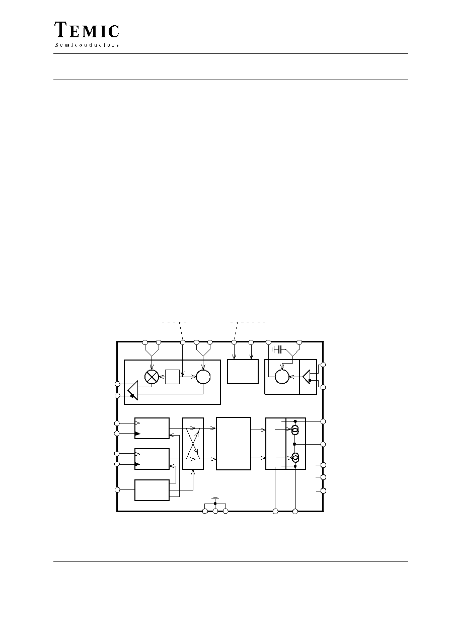
Modulation PLL for GSM, DCS and PCS Systems
Description
The U2893B is a monolithic integrated circuit. It is
realized using TEMIC's advanced silicon bipolar UHF5S
technology. The device integrates a mixer, an I/Q modu-
lator, a phase-frequency detector (PFD) with two
synchronous-programmable dividers, and a charge pump.
The U2893B is designed for cellular phones such as GSM,
DCS1800, and PCS1900, applying a transmitter-archi-
tecture where the VCO is operated at the TX output
frequency.
U2893B exhibits low power consumption, and the power-
down function extends battery life.
The IC is available in a shrinked small-outline 28≠pin
package (SSO28).
Features
D Supply voltage down to 2.7 V
D Current consumption 40 mA
D Power-down function
D Low-current standby mode
D High-speed PFD and charge pump
D Integrated dividers
Benefits
D High-level RF integration
D TX architecture saves filter costs
D Low external part count
D Small SSO28 package
D One device for various applications
Block Diagram
Voltage
reference
PFD
+
I/Q modulator
R : 1
divider
90
grd
MIXLO
VSP
CPO
GNDP
CPC
MDO
NMDO
RD
I
NI
MDLO
NQ
PU MIXO
Q
PUMIX
N : 1
ND
NND
VS3
GND
Mixer
MUX
MC
Mode
control
RF
VS1
VS2
NRD
NRF
12494
divider
Figure 1. Block diagram

U2893B
TELEFUNKEN Semiconductors
Rev. A1, 29-Jan-76
Preliminary Information
2 (14)
Pin Description
1
2
3
4
5
6
7
8
10
9
27
22
21
20
18
19
17
12
11
28
25
26
23
24
NMDO
VS1
VSP
CPO
GNDP
CPC
GND
MDO
PUMIX
MDLO
NI
I
NRF
RF
VS2
MIXLO
PU
GND
MIXO
GND
NND
VS3
NQ
Q
16
15
14
13
12495
RD
NRD
ND
MC
Figure 2. Pinning
Pin
Symbol
Function
¡¡¡
¡¡¡
1
¡¡¡¡¡
¡¡¡¡¡
I
¡¡¡¡¡¡¡¡¡¡
¡¡¡¡¡¡¡¡¡¡
In-phase baseband input
¡¡¡
¡¡¡
2
¡¡¡¡¡
¡¡¡¡¡
NI
¡¡¡¡¡¡¡¡¡¡
¡¡¡¡¡¡¡¡¡¡
Complementary to I
¡¡¡
¡¡¡
3
¡¡¡¡¡
¡¡¡¡¡
MDLO
¡¡¡¡¡¡¡¡¡¡
¡¡¡¡¡¡¡¡¡¡
I/Q-modulator LO input
¡¡¡
¡¡¡
4
¡¡¡¡¡
¡¡¡¡¡
GND
1)
¡¡¡¡¡¡¡¡¡¡
¡¡¡¡¡¡¡¡¡¡
Negative supply
¡¡¡
¡¡¡
5
¡¡¡¡¡
¡¡¡¡¡
MDO
¡¡¡¡¡¡¡¡¡¡
¡¡¡¡¡¡¡¡¡¡
I/Q-modulator output
¡¡¡
¡¡¡
6
¡¡¡¡¡
¡¡¡¡¡
NMDO
¡¡¡¡¡¡¡¡¡¡
¡¡¡¡¡¡¡¡¡¡
Complementary to MDO
¡¡¡
¡¡¡
7
¡¡¡¡¡
¡¡¡¡¡
VS1
3)
¡¡¡¡¡¡¡¡¡¡
¡¡¡¡¡¡¡¡¡¡
Positive supply (I/Q MOD)
¡¡¡
¡¡¡
8
¡¡¡¡¡
¡¡¡¡¡
VSP
¡¡¡¡¡¡¡¡¡¡
¡¡¡¡¡¡¡¡¡¡
Pos. supply charge-pump
¡¡¡
¡¡¡
9
¡¡¡¡¡
¡¡¡¡¡
CPO
¡¡¡¡¡¡¡¡¡¡
¡¡¡¡¡¡¡¡¡¡
Charge-pump output
¡¡¡
¡¡¡
10
¡¡¡¡¡
¡¡¡¡¡
GNDP
2)
¡¡¡¡¡¡¡¡¡¡
¡¡¡¡¡¡¡¡¡¡
Neg. supply charge pump
¡¡¡
¡
¡
¡
11
¡¡¡¡¡
¡
¡¡¡
¡
CPC
¡¡¡¡¡¡¡¡¡¡
¡¡¡¡¡¡¡¡¡
¡
Charge-pump current control
(input)
¡¡¡
¡¡¡
12
¡¡¡¡¡
¡¡¡¡¡
PUMIX
¡¡¡¡¡¡¡¡¡¡
¡¡¡¡¡¡¡¡¡¡
Power-up, mixer only
¡¡¡
¡¡¡
13
¡¡¡¡¡
¡¡¡¡¡
RD
¡¡¡¡¡¡¡¡¡¡
¡¡¡¡¡¡¡¡¡¡
R-divider input
¡¡¡
¡¡¡
14
¡¡¡¡¡
¡¡¡¡¡
NRD
¡¡¡¡¡¡¡¡¡¡
¡¡¡¡¡¡¡¡¡¡
Complementary to RD
¡¡¡
¡¡¡
15
¡¡¡¡¡
¡¡¡¡¡
MC
¡¡¡¡¡¡¡¡¡¡
¡¡¡¡¡¡¡¡¡¡
Mode control
¡¡¡
¡¡¡
16
¡¡¡¡¡
¡¡¡¡¡
ND
¡¡¡¡¡¡¡¡¡¡
¡¡¡¡¡¡¡¡¡¡
N-divider input
¡¡¡
¡¡¡
17
¡¡¡¡¡
¡¡¡¡¡
NND
¡¡¡¡¡¡¡¡¡¡
¡¡¡¡¡¡¡¡¡¡
Complementary to ND
¡¡¡
¡¡¡
18
¡¡¡¡¡
¡¡¡¡¡
GND
1)
¡¡¡¡¡¡¡¡¡¡
¡¡¡¡¡¡¡¡¡¡
Negative supply
¡¡¡
¡¡¡
19
¡¡¡¡¡
¡¡¡¡¡
PU
¡¡¡¡¡¡¡¡¡¡
¡¡¡¡¡¡¡¡¡¡
Power-up, whole chip except
mixer
¡¡¡
¡¡¡
20
¡¡¡¡¡
¡¡¡¡¡
MIXLO
¡¡¡¡¡¡¡¡¡¡
¡¡¡¡¡¡¡¡¡¡
Mixer LO input
¡¡¡
¡¡¡
21
¡¡¡¡¡
¡¡¡¡¡
VS2
3)
¡¡¡¡¡¡¡¡¡¡
¡¡¡¡¡¡¡¡¡¡
Positive supply (MISC.)
¡¡¡
¡¡¡
22
¡¡¡¡¡
¡¡¡¡¡
RF
¡¡¡¡¡¡¡¡¡¡
¡¡¡¡¡¡¡¡¡¡
Mixer RF-input
¡¡¡
¡¡¡
23
¡¡¡¡¡
¡¡¡¡¡
NRF
¡¡¡¡¡¡¡¡¡¡
¡¡¡¡¡¡¡¡¡¡
Complementary to RF
¡¡¡
¡¡¡
24
¡¡¡¡¡
¡¡¡¡¡
GND
1)
¡¡¡¡¡¡¡¡¡¡
¡¡¡¡¡¡¡¡¡¡
Negative supply
¡¡¡
25
¡¡¡¡¡
MIXO
¡¡¡¡¡¡¡¡¡¡
Mixer output
¡¡¡
¡¡¡
26
¡¡¡¡¡
¡¡¡¡¡
VS3
3)
¡¡¡¡¡¡¡¡¡¡
¡¡¡¡¡¡¡¡¡¡
Positive supply (mixer)
¡¡¡
¡¡¡
27
¡¡¡¡¡
¡¡¡¡¡
NQ
¡¡¡¡¡¡¡¡¡¡
¡¡¡¡¡¡¡¡¡¡
Complementary to Q
¡¡¡
¡¡¡
28
¡¡¡¡¡
¡¡¡¡¡
Q
¡¡¡¡¡¡¡¡¡¡
¡¡¡¡¡¡¡¡¡¡
Quad.-phase baseband input
1)
All GND pins must be connected to GND
potential. No DC voltage between GND pins!
2)
Max. voltage between GNDP and GND pins
v 200 mV
3)
The maximum permissible voltage difference
between pins VS1, VS2 and VS3 is 200 mV.

U2893B
Preliminary Information
TELEFUNKEN Semiconductors
Rev. A1, 29-Jan-97
3 (14)
Absolute Maximum Ratings
Parameters
Symbol
Value
Unit
¡¡¡¡¡¡¡¡¡¡¡¡
¡¡¡¡¡¡¡¡¡¡¡¡
Supply voltage VS1, VS2, VS3
¡¡¡¡¡¡¡¡¡
¡¡¡¡¡¡¡¡¡
V
VS#
¡¡¡¡¡¡¡¡¡
¡¡¡¡¡¡¡¡¡
v V
VSP
¡¡¡¡
¡¡¡¡
V
¡¡¡¡¡¡¡¡¡¡¡¡
¡¡¡¡¡¡¡¡¡¡¡¡
Supply voltage charge pump VSP
¡¡¡¡¡¡¡¡¡
¡¡¡¡¡¡¡¡¡
V
VSP
¡¡¡¡¡¡¡¡¡
¡¡¡¡¡¡¡¡¡
5.5
¡¡¡¡
¡¡¡¡
V
¡¡¡¡¡¡¡¡¡¡¡¡
¡¡¡¡¡¡¡¡¡¡¡¡
Voltage at any input
¡¡¡¡¡¡¡¡¡
¡¡¡¡¡¡¡¡¡
V
Vi#
¡¡¡¡¡¡¡¡¡
¡¡¡¡¡¡¡¡¡
≠0.5
v V
VS
+0.5
v 5.5
¡¡¡¡
¡¡¡¡
V
¡¡¡¡¡¡¡¡¡¡¡¡
¡
¡¡¡¡¡¡¡¡¡¡
¡
¡¡¡¡¡¡¡¡¡¡¡¡
Current at any input / output pin
except CPC
¡¡¡¡¡¡¡¡¡
¡
¡¡¡¡¡¡¡
¡
¡¡¡¡¡¡¡¡¡
| I
I#
| | I
O#
|
¡¡¡¡¡¡¡¡¡
¡
¡¡¡¡¡¡¡
¡
¡¡¡¡¡¡¡¡¡
2
¡¡¡¡
¡
¡¡
¡
¡¡¡¡
mA
¡¡¡¡¡¡¡¡¡¡¡¡
¡¡¡¡¡¡¡¡¡¡¡¡
CPC output currents
¡¡¡¡¡¡¡¡¡
¡¡¡¡¡¡¡¡¡
| I
CPC
|
¡¡¡¡¡¡¡¡¡
¡¡¡¡¡¡¡¡¡
5
¡¡¡¡
¡¡¡¡
mA
¡¡¡¡¡¡¡¡¡¡¡¡
Ambient temperature
¡¡¡¡¡¡¡¡¡
T
amb
¡¡¡¡¡¡¡¡¡
≠20 to +85
¡¡¡¡
∞
C
¡¡¡¡¡¡¡¡¡¡¡¡
¡¡¡¡¡¡¡¡¡¡¡¡
Storage temperature
¡¡¡¡¡¡¡¡¡
¡¡¡¡¡¡¡¡¡
T
stg
¡¡¡¡¡¡¡¡¡
¡¡¡¡¡¡¡¡¡
≠40 to +125
¡¡¡¡
¡¡¡¡
∞
C
Operating Range
Parameters
Symbol
Value
Unit
¡¡¡¡¡¡¡¡¡¡¡¡
¡¡¡¡¡¡¡¡¡¡¡¡
Supply voltage
¡¡¡¡¡¡¡¡¡
¡¡¡¡¡¡¡¡¡
V
VS#
, V
VSP
¡¡¡¡¡¡¡¡¡
¡¡¡¡¡¡¡¡¡
2.7 to 5.5
¡¡¡¡
¡¡¡¡
V
¡¡¡¡¡¡¡¡¡¡¡¡
¡¡¡¡¡¡¡¡¡¡¡¡
Ambient temperature
¡¡¡¡¡¡¡¡¡
¡¡¡¡¡¡¡¡¡
T
amb
¡¡¡¡¡¡¡¡¡
¡¡¡¡¡¡¡¡¡
≠20 to +85
¡¡¡¡
¡¡¡¡
∞
C
Thermal Resistance
Parameters
Symbol
Value
Unit
¡¡¡¡¡¡¡¡¡¡¡¡
¡¡¡¡¡¡¡¡¡¡¡¡
Junction ambient SSO28
¡¡¡¡¡¡¡¡¡
¡¡¡¡¡¡¡¡¡
R
thJA
¡¡¡¡¡¡¡¡¡
¡¡¡¡¡¡¡¡¡
130
¡¡¡¡
¡¡¡¡
K/W
Electrical Characteristics: General Data
T
amb
= 25
∞
C, V
S
= 2.7 to 5.5 V
Parameters
Test Conditions / Pin
Symbol
Min.
Typ.
Max.
Unit
¡¡¡¡¡¡¡¡¡¡¡¡¡¡¡¡¡¡¡¡¡¡¡¡¡¡¡¡¡¡¡¡
¡¡¡¡¡¡¡¡¡¡¡¡¡¡¡¡¡¡¡¡¡¡¡¡¡¡¡¡¡¡¡¡
DC supply
¡¡¡¡¡¡¡¡
¡¡¡¡¡¡¡¡
Supply voltages VS#
¡¡¡¡¡¡¡¡¡
¡¡¡¡¡¡¡¡¡
V
VS1
= V
VS2
= V
VS3
¡¡¡¡¡¡
¡¡¡¡¡¡
V
VS#
¡¡¡¡
¡¡¡¡
2.7
¡¡¡
¡¡¡
¡¡¡¡
¡¡¡¡
5.5
¡¡¡¡
¡¡¡¡
V
¡¡¡¡¡¡¡¡
¡
¡¡¡¡¡¡
¡
¡¡¡¡¡¡¡¡
Supply voltage VSP
¡¡¡¡¡¡¡¡¡
¡
¡¡¡¡¡¡¡
¡
¡¡¡¡¡¡¡¡¡
¡¡¡¡¡¡
¡
¡¡¡¡
¡
¡¡¡¡¡¡
V
VSP
¡¡¡¡
¡
¡¡
¡
¡¡¡¡
V
VS#
≠ 0.3
¡¡¡
¡¡
¡
¡¡¡
¡¡¡¡
¡
¡¡
¡
¡¡¡¡
5.5
¡¡¡¡
¡
¡¡
¡
¡¡¡¡
V
¡¡¡¡¡¡¡¡
¡¡¡¡¡¡¡¡
Supply current I
VS1
¡¡¡¡¡¡¡¡¡
¡¡¡¡¡¡¡¡¡
Active (V
PU
= VS)
¡¡¡¡¡¡
¡¡¡¡¡¡
I
VS1A
¡¡¡¡
¡¡¡¡
¡¡¡
¡¡¡
16
¡¡¡¡
¡¡¡¡
¡¡¡¡
¡¡¡¡
mA
¡¡¡¡¡¡¡¡
¡¡¡¡¡¡¡¡
pp y
VS1
¡¡¡¡¡¡¡¡¡
¡¡¡¡¡¡¡¡¡
Standby (V
PU
= 0)
¡¡¡¡¡¡
¡¡¡¡¡¡
I
VS1Y
¡¡¡¡
¡¡¡¡
¡¡¡
¡¡¡
¡¡¡¡
¡¡¡¡
20
¡¡¡¡
¡¡¡¡
mA
¡¡¡¡¡¡¡¡
¡¡¡¡¡¡¡¡
Supply current I
VS2
¡¡¡¡¡¡¡¡¡
¡¡¡¡¡¡¡¡¡
Active (V
PU
= VS)
¡¡¡¡¡¡
¡¡¡¡¡¡
I
VS2A
¡¡¡¡
¡¡¡¡
¡¡¡
¡¡¡
21
¡¡¡¡
¡¡¡¡
¡¡¡¡
¡¡¡¡
mA
¡¡¡¡¡¡¡¡
¡¡¡¡¡¡¡¡
pp y
VS2
¡¡¡¡¡¡¡¡¡
¡¡¡¡¡¡¡¡¡
Standby (V
PU
= 0)
¡¡¡¡¡¡
¡¡¡¡¡¡
I
VS2Y
¡¡¡¡
¡¡¡¡
¡¡¡
¡¡¡
¡¡¡¡
¡¡¡¡
20
¡¡¡¡
¡¡¡¡
mA
¡¡¡¡¡¡¡¡
¡¡¡¡¡¡¡¡
Supply current I
VS3
¡¡¡¡¡¡¡¡¡
¡¡¡¡¡¡¡¡¡
Active (V
PUMIX
= VS)
¡¡¡¡¡¡
¡¡¡¡¡¡
I
VS3A
¡¡¡¡
¡¡¡¡
¡¡¡
¡¡¡
11
¡¡¡¡
¡¡¡¡
¡¡¡¡
¡¡¡¡
mA
¡¡¡¡¡¡¡¡
¡¡¡¡¡¡¡¡
pp y
VS3
¡¡¡¡¡¡¡¡¡
¡¡¡¡¡¡¡¡¡
Standby (V
PUMIX
= 0)
¡¡¡¡¡¡
¡¡¡¡¡¡
I
VS3Y
¡¡¡¡
¡¡¡¡
¡¡¡
¡¡¡
¡¡¡¡
¡¡¡¡
30
¡¡¡¡
¡¡¡¡
mA
¡¡¡¡¡¡¡¡
¡
¡¡¡¡¡¡
¡
¡¡¡¡¡¡¡¡
Supply current I
VSP
1)
¡¡¡¡¡¡¡¡¡
¡
¡¡¡¡¡¡¡
¡
¡¡¡¡¡¡¡¡¡
Active
(V
PU
= VS, CPO open)
¡¡¡¡¡¡
¡
¡¡¡¡
¡
¡¡¡¡¡¡
I
VSPA
¡¡¡¡
¡
¡¡
¡
¡¡¡¡
¡¡¡
¡¡
¡
¡¡¡
2)
¡¡¡¡
¡
¡¡
¡
¡¡¡¡
20
¡¡¡¡
¡
¡¡
¡
¡¡¡¡
mA
¡¡¡¡¡¡¡¡
¡¡¡¡¡¡¡¡
¡¡¡¡¡¡¡¡¡
¡¡¡¡¡¡¡¡¡
Standby (V
PU
= 0)
¡¡¡¡¡¡
¡¡¡¡¡¡
I
VSPY
¡¡¡¡
¡¡¡¡
¡¡¡
¡¡¡
¡¡¡¡
¡¡¡¡
20
¡¡¡¡
¡¡¡¡
mA
¡¡¡¡¡¡¡¡¡¡¡¡¡¡¡¡¡¡¡¡¡¡¡¡¡¡¡¡¡¡¡¡
¡¡¡¡¡¡¡¡¡¡¡¡¡¡¡¡¡¡¡¡¡¡¡¡¡¡¡¡¡¡¡¡
N & R divider inputs ND, NND & RD, NRD
¡¡¡¡¡¡¡¡
¡¡¡¡¡¡¡¡
N:1 divider frequency
¡¡¡¡¡¡¡¡¡
¡¡¡¡¡¡¡¡¡
50-
W source
¡¡¡¡¡¡
¡¡¡¡¡¡
F
ND
¡¡¡¡
¡¡¡¡
100
¡¡¡
¡¡¡
¡¡¡¡
¡¡¡¡
650
¡¡¡¡
¡¡¡¡
MHz
¡¡¡¡¡¡¡¡
¡¡¡¡¡¡¡¡
R:1 divider frequency
¡¡¡¡¡¡¡¡¡
¡¡¡¡¡¡¡¡¡
50-
W source
¡¡¡¡¡¡
¡¡¡¡¡¡
F
RD
¡¡¡¡
¡¡¡¡
100
¡¡¡
¡¡¡
¡¡¡¡
¡¡¡¡
400
¡¡¡¡
¡¡¡¡
MHz
¡¡¡¡¡¡¡¡
¡¡¡¡¡¡¡¡
Input impedance
¡¡¡¡¡¡¡¡¡
¡¡¡¡¡¡¡¡¡
Active & standby
¡¡¡¡¡¡
¡¡¡¡¡¡
Z
RD
, Z
ND
¡¡¡¡
¡¡¡¡
1 k
¡¡¡
¡¡¡
¡¡¡¡
¡¡¡¡
2 pF
¡¡¡¡
¡¡¡¡
≠
¡¡¡¡¡¡¡¡
¡¡¡¡¡¡¡¡
Input sensitivity
¡¡¡¡¡¡¡¡¡
¡¡¡¡¡¡¡¡¡
50-
W source
¡¡¡¡¡¡
¡¡¡¡¡¡
V
RDeff
, V
NDeff
¡¡¡¡
¡¡¡¡
30
¡¡¡
¡¡¡
¡¡¡¡
¡¡¡¡
200
¡¡¡¡
¡¡¡¡
mV
1)
100-MHz PFD operation, pump current set to 4 mA, zero phase difference (steady state)
2)
See chapter "Supply Current of the Charge Pump i(VSP) vs. Time", page 6.

U2893B
TELEFUNKEN Semiconductors
Rev. A1, 29-Jan-76
Preliminary Information
4 (14)
Electrical Characteristics: General Data (continued)
T
amb
= 25
∞
C, V
S
= 2.7 to 5.5 V
Parameters
Test Conditions / Pin
Symbol
Min.
Typ.
Max.
Unit
¡¡¡¡¡¡¡¡¡¡¡¡¡¡¡¡¡¡¡¡¡¡¡¡¡¡¡¡¡¡¡¡
¡¡¡¡¡¡¡¡¡¡¡¡¡¡¡¡¡¡¡¡¡¡¡¡¡¡¡¡¡¡¡¡
Phase-frequency detector (PFD)
¡¡¡¡¡¡¡¡
¡
¡¡¡¡¡¡
¡
PFD operation
¡¡¡¡¡¡¡¡
¡
¡¡¡¡¡¡
¡
F
ND
= 650 MHz, n = 5
F
RD
= 300 MHz, r = 2
¡¡¡¡¡¡¡
¡
¡¡¡¡¡
¡
FM
PFD
¡¡¡
¡
¡
¡
150
¡¡¡¡
¡
¡¡
¡
¡¡¡¡
¡
¡¡
¡
¡¡¡¡
¡
¡¡
¡
MHz
¡¡¡¡¡¡¡¡
¡
¡¡¡¡¡¡
¡
¡¡¡¡¡¡¡¡
Frequency comparison
only
¡¡¡¡¡¡¡¡
¡
¡¡¡¡¡¡
¡
¡¡¡¡¡¡¡¡
F
ND
= 650 MHz, n = 5
F
RD
= 300 MHz, r = 2
¡¡¡¡¡¡¡
¡
¡¡¡¡¡
¡
¡¡¡¡¡¡¡
FM
FD
¡¡¡
¡
¡
¡
¡¡¡
200
¡¡¡¡
¡
¡¡
¡
¡¡¡¡
¡¡¡¡
¡
¡¡
¡
¡¡¡¡
¡¡¡¡
¡
¡¡
¡
¡¡¡¡
MHz
¡¡¡¡¡¡¡¡¡¡¡¡¡¡¡¡¡¡¡¡¡¡¡¡¡¡¡¡¡¡¡¡
¡¡¡¡¡¡¡¡¡¡¡¡¡¡¡¡¡¡¡¡¡¡¡¡¡¡¡¡¡¡¡¡
I/Q modulator baseband inputs I, NI & Q, NQ
¡¡¡¡¡¡¡¡
¡
¡¡¡¡¡¡
¡
¡¡¡¡¡¡¡¡
DC voltage
¡¡¡¡¡¡¡¡
¡
¡¡¡¡¡¡
¡
¡¡¡¡¡¡¡¡
Referred to GND
¡¡¡¡¡¡¡
¡
¡¡¡¡¡
¡
¡¡¡¡¡¡¡
V
I,
V
NI,
V
Q,
V
NQ
¡¡¡
¡
¡
¡
¡¡¡
1.35
¡¡¡¡
¡
¡¡
¡
¡¡¡¡
VS1/2
¡¡¡¡
¡
¡¡
¡
¡¡¡¡
VS1/2
+ 0.1
¡¡¡¡
¡
¡¡
¡
¡¡¡¡
V
¡¡¡¡¡¡¡¡
MD_IQ
¡¡¡¡¡¡¡¡
Frequency range
¡¡¡¡¡¡¡
FR
IO
¡¡¡
DC
¡¡¡¡
¡¡¡¡
1
¡¡¡¡
MHz
¡¡¡¡¡¡¡¡
¡
¡¡¡¡¡¡
¡
¡¡¡¡¡¡¡¡
AC voltage
3)
¡¡¡¡¡¡¡¡
¡
¡¡¡¡¡¡
¡
¡¡¡¡¡¡¡¡
Referred to GND
¡¡¡¡¡¡¡
¡
¡¡¡¡¡
¡
¡¡¡¡¡¡¡
AC
I,
AC
NI,
AC
Q,
AC
NQ
¡¡¡
¡
¡
¡
¡¡¡
¡¡¡¡
¡
¡¡
¡
¡¡¡¡
200
¡¡¡¡
¡
¡¡
¡
¡¡¡¡
¡¡¡¡
¡
¡¡
¡
¡¡¡¡
mVpp
¡¡¡¡¡¡¡¡
¡¡¡¡¡¡¡¡
¡¡¡¡¡¡¡¡
¡¡¡¡¡¡¡¡
Differential (preferres)
¡¡¡¡¡¡¡
¡¡¡¡¡¡¡
AC
DI,
AC
DQ
¡¡¡
¡¡¡
¡¡¡¡
¡¡¡¡
400
¡¡¡¡
¡¡¡¡
¡¡¡¡
¡¡¡¡
mVpp
¡¡¡¡¡¡¡¡¡¡¡¡¡¡¡¡¡¡¡¡¡¡¡¡¡¡¡¡¡¡¡¡
¡¡¡¡¡¡¡¡¡¡¡¡¡¡¡¡¡¡¡¡¡¡¡¡¡¡¡¡¡¡¡¡
I/Q modulator LO input MDLO
¡¡¡¡¡¡¡¡
¡¡¡¡¡¡¡¡
MDLO
¡¡¡¡¡¡¡¡
¡¡¡¡¡¡¡¡
Frequency range
¡¡¡¡¡¡¡
¡¡¡¡¡¡¡
F
MDLO
¡¡¡
¡¡¡
50
¡¡¡¡
¡¡¡¡
¡¡¡¡
¡¡¡¡
350
¡¡¡¡
¡¡¡¡
MHz
¡¡¡¡¡¡¡¡
¡¡¡¡¡¡¡¡
Input impedance
¡¡¡¡¡¡¡¡
¡¡¡¡¡¡¡¡
Active & standby
¡¡¡¡¡¡¡
¡¡¡¡¡¡¡
Z
MDLO
¡¡¡
¡¡¡
¡¡¡¡
¡¡¡¡
250
¡¡¡¡
¡¡¡¡
¡¡¡¡
¡¡¡¡
W
¡¡¡¡¡¡¡¡
Input level
¡¡¡¡¡¡¡¡
50-
W source
¡¡¡¡¡¡¡
P
MDLO
¡¡¡
¡¡¡¡
≠12
¡¡¡¡
≠5
¡¡¡¡
dBm
¡¡¡¡¡¡¡¡¡¡¡¡¡¡¡¡¡¡¡¡¡¡¡¡¡¡¡¡¡¡¡¡
¡¡¡¡¡¡¡¡¡¡¡¡¡¡¡¡¡¡¡¡¡¡¡¡¡¡¡¡¡¡¡¡
I/Q modulator outputs MDO, NMDO
¡¡¡¡¡¡¡¡
¡¡¡¡¡¡¡¡
DC current
¡¡¡¡¡¡¡¡
¡¡¡¡¡¡¡¡
V
MDO
, V
NMDO
= VS
¡¡¡¡¡¡¡
¡¡¡¡¡¡¡
I
MDO
, I
NMDO
¡¡¡
¡¡¡
¡¡¡¡
¡¡¡¡
2.4
¡¡¡¡
¡¡¡¡
¡¡¡¡
¡¡¡¡
mA
¡¡¡¡¡¡¡¡
¡¡¡¡¡¡¡¡
Voltage compliance
¡¡¡¡¡¡¡¡
¡¡¡¡¡¡¡¡
V
MDO
, V
NMDO
= VC
¡¡¡¡¡¡¡
¡¡¡¡¡¡¡
VC
MDO
, VC
NMDO
¡¡¡
¡¡¡
¡¡¡¡
¡¡¡¡
¡¡¡¡
¡¡¡¡
¡¡¡¡
¡¡¡¡
¡¡¡¡¡¡¡¡
¡
¡¡¡¡¡¡
¡
¡¡¡¡¡¡¡¡
MDO output level
(differential)
¡¡¡¡¡¡¡¡
¡
¡¡¡¡¡¡
¡
¡¡¡¡¡¡¡¡
500
W to VS
4)
¡¡¡¡¡¡¡
¡
¡¡¡¡¡
¡
¡¡¡¡¡¡¡
P
MDOeff
¡¡¡
¡
¡
¡
¡¡¡
120
¡¡¡¡
¡
¡¡
¡
¡¡¡¡
¡¡¡¡
¡
¡¡
¡
¡¡¡¡
150
¡¡¡¡
¡
¡¡
¡
¡¡¡¡
mV
¡¡¡¡¡¡¡¡
¡¡¡¡¡¡¡¡
Carrier suppression
4)
¡¡¡¡¡¡¡¡
¡¡¡¡¡¡¡¡
¡¡¡¡¡¡¡
¡¡¡¡¡¡¡
CS
MDO
¡¡¡
¡¡¡
≠30
¡¡¡¡
¡¡¡¡
≠35
¡¡¡¡
¡¡¡¡
¡¡¡¡
¡¡¡¡
dBc
¡¡¡¡¡¡¡¡
Sideband suppression
4)
¡¡¡¡¡¡¡¡
¡¡¡¡¡¡¡
SS
MDO
¡¡¡
≠35
¡¡¡¡
≠40
¡¡¡¡
¡¡¡¡
dBc
¡¡¡¡¡¡¡¡
¡¡¡¡¡¡¡¡
IF spurious
4)
¡¡¡¡¡¡¡¡
¡¡¡¡¡¡¡¡
f_LO +/≠ 3
f_mod
¡¡¡¡¡¡¡
¡¡¡¡¡¡¡
SP
MDO
¡¡¡
¡¡¡
≠45
¡¡¡¡
¡¡¡¡
≠50
¡¡¡¡
¡¡¡¡
¡¡¡¡
¡¡¡¡
dBc
¡¡¡¡¡¡¡¡
¡¡¡¡¡¡¡¡
Noise
4)
¡¡¡¡¡¡¡¡
¡¡¡¡¡¡¡¡
@ 400 kHz off carrier
¡¡¡¡¡¡¡
¡¡¡¡¡¡¡
N
MDO
¡¡¡
¡¡¡
≠115
¡¡¡¡
¡¡¡¡
¡¡¡¡
¡¡¡¡
¡¡¡¡
¡¡¡¡
dBc/Hz
¡¡¡¡¡¡¡¡
¡¡¡¡¡¡¡¡
Frequency range
¡¡¡¡¡¡¡¡
¡¡¡¡¡¡¡¡
¡¡¡¡¡¡¡
¡¡¡¡¡¡¡
FR
MDO
¡¡¡
¡¡¡
50
¡¡¡¡
¡¡¡¡
¡¡¡¡
¡¡¡¡
350
¡¡¡¡
¡¡¡¡
MHz
¡¡¡¡¡¡¡¡¡¡¡¡¡¡¡¡¡¡¡¡¡¡¡¡¡¡¡¡¡¡¡¡
¡¡¡¡¡¡¡¡¡¡¡¡¡¡¡¡¡¡¡¡¡¡¡¡¡¡¡¡¡¡¡¡
Mixer (900 MHz)
¡¡¡¡¡¡¡¡
¡¡¡¡¡¡¡¡
RF input level
¡¡¡¡¡¡¡¡
¡¡¡¡¡¡¡¡
900 MHz
¡¡¡¡¡¡¡
¡¡¡¡¡¡¡
P9
RF
¡¡¡
¡¡¡
tbd
¡¡¡¡
¡¡¡¡
≠15
¡¡¡¡
¡¡¡¡
¡¡¡¡
¡¡¡¡
dBm
¡¡¡¡¡¡¡¡
¡¡¡¡¡¡¡¡
LO-spurious at
RF/NRF port
¡¡¡¡¡¡¡¡
¡¡¡¡¡¡¡¡
@ P9
MIXLO
= ≠10 dBm
@ P9
RF
= ≠15 dBm
¡¡¡¡¡¡¡
¡¡¡¡¡¡¡
SP9
RF
¡¡¡
¡¡¡
¡¡¡¡
¡¡¡¡
¡¡¡¡
¡¡¡¡
≠40
¡¡¡¡
¡¡¡¡
dBm
¡¡¡¡¡¡¡¡
¡¡¡¡¡¡¡¡
MIXLO input level
¡¡¡¡¡¡¡¡
¡¡¡¡¡¡¡¡
0.05 to 2 GHz
¡¡¡¡¡¡¡
¡¡¡¡¡¡¡
P9
MIXLO
¡¡¡
¡¡¡
tbd
¡¡¡¡
¡¡¡¡
≠10
¡¡¡¡
¡¡¡¡
¡¡¡¡
¡¡¡¡
dBm
¡¡¡¡¡¡¡¡
¡¡¡¡¡¡¡¡
MIXO (100-
W load)
¡¡¡¡¡¡¡¡
¡¡¡¡¡¡¡¡
Frequency range
¡¡¡¡¡¡¡
¡¡¡¡¡¡¡
FR
MIXO
¡¡¡
¡¡¡
50
¡¡¡¡
¡¡¡¡
¡¡¡¡
¡¡¡¡
350
¡¡¡¡
¡¡¡¡
MHz
¡¡¡¡¡¡¡¡
¡¡¡¡¡¡¡¡
... Output level
5)
¡¡¡¡¡¡¡¡
¡¡¡¡¡¡¡¡
@ P9
MIXLO
= ≠15 dBm
¡¡¡¡¡¡¡
¡¡¡¡¡¡¡
P9
MIXOeff
¡¡¡
¡¡¡
¡¡¡¡
¡¡¡¡
70
¡¡¡¡
¡¡¡¡
¡¡¡¡
¡¡¡¡
mV
¡¡¡¡¡¡¡¡
¡¡¡¡¡¡¡¡
... Carrier suppression
¡¡¡¡¡¡¡¡
¡¡¡¡¡¡¡¡
@ P9
MIXLO
= ≠15 dBm
¡¡¡¡¡¡¡
¡¡¡¡¡¡¡
CS9
MIXO
¡¡¡
¡¡¡
≠20
¡¡¡¡
¡¡¡¡
¡¡¡¡
¡¡¡¡
¡¡¡¡
¡¡¡¡
dBc
3)
Single-ended operation (complementary baseband input is AC-grounded) leads to reduced linearity degrading
suppression of odd harmonics
4)
With typical drive levels at MDLO- & I/Q-inputs
5)
≠1 dB compression point (CP-1)
U2893B
Preliminary Information
TELEFUNKEN Semiconductors
Rev. A1, 29-Jan-97
5 (14)
Electrical Characteristics: General Data (continued)
T
amb
= 25
∞
C, V
S
= 2.7 to 5.5 V
Parameters
Test Conditions / Pin
Symbol
Min.
Typ.
Max.
Unit
¡¡¡¡¡¡¡¡¡¡¡¡¡¡¡¡¡¡¡¡¡¡¡¡¡¡¡¡¡¡¡¡
¡¡¡¡¡¡¡¡¡¡¡¡¡¡¡¡¡¡¡¡¡¡¡¡¡¡¡¡¡¡¡¡
Mixer (1900 MHz)
¡¡¡¡¡¡¡¡
¡¡¡¡¡¡¡¡
RF input level
¡¡¡¡¡¡¡¡¡
¡¡¡¡¡¡¡¡¡
0.5 to 2 GHz
¡¡¡¡¡¡
¡¡¡¡¡¡
P19
RF
¡¡¡¡
¡¡¡¡
¡¡¡
¡¡¡
≠17
¡¡¡¡
¡¡¡¡
¡¡¡¡
¡¡¡¡
dBm
¡¡¡¡¡¡¡¡
¡¡¡¡¡¡¡¡
LO-spurious at
RF/NRF ports
¡¡¡¡¡¡¡¡¡
¡¡¡¡¡¡¡¡¡
@ P19
MIXLO
= ≠10 dBm
@ P19
RF
= ≠15 dBm
¡¡¡¡¡¡
¡¡¡¡¡¡
SP19
RF
¡¡¡¡
¡¡¡¡
¡¡¡
¡¡¡
¡¡¡¡
¡¡¡¡
≠40
¡¡¡¡
¡¡¡¡
dBm
¡¡¡¡¡¡¡¡
¡¡¡¡¡¡¡¡
MIXLO input level
¡¡¡¡¡¡¡¡¡
¡¡¡¡¡¡¡¡¡
0.05 to 2 GHz
¡¡¡¡¡¡
¡¡¡¡¡¡
P19
MIXLO
¡¡¡¡
¡¡¡¡
¡¡¡
¡¡¡
≠8
¡¡¡¡
¡¡¡¡
¡¡¡¡
¡¡¡¡
dBm
¡¡¡¡¡¡¡¡
¡¡¡¡¡¡¡¡
MIXO (100
W load)
¡¡¡¡¡¡¡¡¡
¡¡¡¡¡¡¡¡¡
¡¡¡¡¡¡
¡¡¡¡¡¡
¡¡¡¡
¡¡¡¡
¡¡¡
¡¡¡
¡¡¡¡
¡¡¡¡
¡¡¡¡
¡¡¡¡
¡¡¡¡¡¡¡¡
¡¡¡¡¡¡¡¡
... Output level
5)
¡¡¡¡¡¡¡¡¡
¡¡¡¡¡¡¡¡¡
@ P19
MIXLO
= ≠17 dBm
¡¡¡¡¡¡
¡¡¡¡¡¡
P19
MIXO
¡¡¡¡
¡¡¡¡
¡¡¡
¡¡¡
55
¡¡¡¡
¡¡¡¡
¡¡¡¡
¡¡¡¡
mVeff
¡¡¡¡¡¡¡¡
¡¡¡¡¡¡¡¡
... Carrier suppression
¡¡¡¡¡¡¡¡¡
¡¡¡¡¡¡¡¡¡
@ P19
MIXLO
= ≠17 dBm
¡¡¡¡¡¡
¡¡¡¡¡¡
CS19
MIXO
¡¡¡¡
¡¡¡¡
≠20
¡¡¡
¡¡¡
¡¡¡¡
¡¡¡¡
¡¡¡¡
¡¡¡¡
dBc
¡¡¡¡¡¡¡¡¡¡¡¡¡¡¡¡¡¡¡¡¡¡¡¡¡¡¡¡¡¡¡¡
¡¡¡¡¡¡¡¡¡¡¡¡¡¡¡¡¡¡¡¡¡¡¡¡¡¡¡¡¡¡¡¡
Charge pump output CPO
¡¡¡¡¡¡¡¡
¡¡¡¡¡¡¡¡
Pump current pulse
¡¡¡¡¡¡¡¡¡
¡¡¡¡¡¡¡¡¡
CPC open
¡¡¡¡¡¡
¡¡¡¡¡¡
| I
CPO
|
¡¡¡¡
¡¡¡¡
0.8
¡¡¡
¡¡¡
1
¡¡¡¡
¡¡¡¡
1.2
¡¡¡¡
¡¡¡¡
mA
¡¡¡¡¡¡¡¡
p
p
¡¡¡¡¡¡¡¡¡
2.23 k
CPC to GND
¡¡¡¡¡¡
| I
CPO 2
|
¡¡¡¡
1.6
¡¡¡
2
¡¡¡¡
2.4
¡¡¡¡
mA
¡¡¡¡¡¡¡¡
¡¡¡¡¡¡¡¡
¡¡¡¡¡¡¡¡¡
¡¡¡¡¡¡¡¡¡
760
CPC to GND
¡¡¡¡¡¡
¡¡¡¡¡¡
| I
CPO_4
|
¡¡¡¡
¡¡¡¡
3.6
¡¡¡
¡¡¡
4
¡¡¡¡
¡¡¡¡
4.4
¡¡¡¡
¡¡¡¡
mA
¡¡¡¡¡¡¡¡
¡¡¡¡¡¡¡¡
TK pump current
¡¡¡¡¡¡¡¡¡
¡¡¡¡¡¡¡¡¡
¡¡¡¡¡¡
¡¡¡¡¡¡
Tk_| I
CPC
|
¡¡¡¡
¡¡¡¡
¡¡¡
¡¡¡
¡¡¡¡
¡¡¡¡
15
¡¡¡¡
¡¡¡¡
%/100 k
¡¡¡¡¡¡¡¡
¡
¡¡¡¡¡¡
¡
¡
¡¡¡¡¡¡
¡
¡¡¡¡¡¡¡¡
Mismatch source / sink
current
¡¡¡¡¡¡¡¡¡
¡
¡¡¡¡¡¡¡
¡
¡
¡¡¡¡¡¡¡
¡
¡¡¡¡¡¡¡¡¡
(I
CPOSI
≠ I
CPOSO
)/I
CPOSI
I
CPOSO
= I
sourc
I
CPOSI
= I
sink
¡¡¡¡¡¡
¡
¡¡¡¡
¡
¡
¡¡¡¡
¡
¡¡¡¡¡¡
M
ICPO
¡¡¡¡
¡
¡¡
¡
¡
¡¡
¡
¡¡¡¡
¡¡¡
¡¡
¡
¡¡
¡
¡¡¡
¡¡¡¡
¡
¡¡
¡
¡
¡¡
¡
¡¡¡¡
10
¡¡¡¡
¡
¡¡
¡
¡
¡¡
¡
¡¡¡¡
%
¡¡¡¡¡¡¡¡
¡
¡¡¡¡¡¡
¡
¡¡¡¡¡¡¡¡
Sensivity to VSP
|
DI
CPO
I
CPO
|
| D
VSP
VSP
|
¡¡¡¡¡¡
¡
¡¡¡¡
¡
¡¡¡¡¡¡
S
ICPO
¡¡¡¡
¡
¡¡
¡
¡¡¡¡
¡¡¡
¡¡
¡
¡¡¡
¡¡¡¡
¡
¡¡
¡
¡¡¡¡
0.1
¡¡¡¡
¡
¡¡
¡
¡¡¡¡
≠
¡¡¡¡¡¡¡¡¡¡¡¡¡¡¡¡¡¡¡¡¡¡¡¡¡¡¡¡¡¡¡¡
Charge pump control input CPC
¡¡¡¡¡¡¡¡
¡¡¡¡¡¡¡¡
Compensation capacitor
¡¡¡¡¡¡¡¡¡
¡¡¡¡¡¡¡¡¡
¡¡¡¡¡¡
¡¡¡¡¡¡
C
CPC
¡¡¡¡
¡¡¡¡
500
¡¡¡
¡¡¡
¡¡¡¡
¡¡¡¡
¡¡¡¡
¡¡¡¡
pF
¡¡¡¡¡¡¡¡
¡¡¡¡¡¡¡¡
Short circuit current
6)
¡¡¡¡¡¡¡¡¡
¡¡¡¡¡¡¡¡¡
CPC grounded
¡¡¡¡¡¡
¡¡¡¡¡¡
| I
CPCK
|
¡¡¡¡
¡¡¡¡
2
¡¡¡
¡¡¡
2.7
¡¡¡¡
¡¡¡¡
3.7
¡¡¡¡
¡¡¡¡
mA
¡¡¡¡¡¡¡¡¡¡¡¡¡¡¡¡¡¡¡¡¡¡¡¡¡¡¡¡¡¡¡¡
¡¡¡¡¡¡¡¡¡¡¡¡¡¡¡¡¡¡¡¡¡¡¡¡¡¡¡¡¡¡¡¡
Mode control
¡¡¡¡¡¡¡¡
¡¡¡¡¡¡¡¡
Sink current
¡¡¡¡¡¡¡¡¡
¡¡¡¡¡¡¡¡¡
V
MC
= VS
¡¡¡¡¡¡
¡¡¡¡¡¡
I
MC
¡¡¡¡
¡¡¡¡
¡¡¡
¡¡¡
20
¡¡¡¡
¡¡¡¡
¡¡¡¡
¡¡¡¡
mA
¡¡¡¡¡¡¡¡¡¡¡¡¡¡¡¡¡¡¡¡¡¡¡¡¡¡¡¡¡¡¡¡
¡¡¡¡¡¡¡¡¡¡¡¡¡¡¡¡¡¡¡¡¡¡¡¡¡¡¡¡¡¡¡¡
Power-up input PU (power-up for all functions, except mixer)
¡¡¡¡¡¡¡¡
¡
¡¡¡¡¡¡
¡
¡¡¡¡¡¡¡¡
Settling time
¡¡¡¡¡¡¡¡¡
¡
¡¡¡¡¡¡¡
¡
¡¡¡¡¡¡¡¡¡
Output power within
10% of steady state
values
¡¡¡¡¡¡
¡
¡¡¡¡
¡
¡¡¡¡¡¡
S
PU
¡¡¡¡
¡
¡¡
¡
¡¡¡¡
¡¡¡
¡¡
¡
¡¡¡
5
¡¡¡¡
¡
¡¡
¡
¡¡¡¡
10
¡¡¡¡
¡
¡¡
¡
¡¡¡¡
ms
¡¡¡¡¡¡¡¡
¡¡¡¡¡¡¡¡
High level
¡¡¡¡¡¡¡¡¡
¡¡¡¡¡¡¡¡¡
Active
¡¡¡¡¡¡
¡¡¡¡¡¡
V
PUH
¡¡¡¡
¡¡¡¡
2.5
¡¡¡
¡¡¡
¡¡¡¡
¡¡¡¡
¡¡¡¡
¡¡¡¡
V
¡¡¡¡¡¡¡¡
¡¡¡¡¡¡¡¡
Low level
¡¡¡¡¡¡¡¡¡
¡¡¡¡¡¡¡¡¡
Standby
¡¡¡¡¡¡
¡¡¡¡¡¡
V
PUL
¡¡¡¡
¡¡¡¡
0
¡¡¡
¡¡¡
¡¡¡¡
¡¡¡¡
0.4
¡¡¡¡
¡¡¡¡
V
¡¡¡¡¡¡¡¡
¡¡¡¡¡¡¡¡
High-level current
¡¡¡¡¡¡¡¡¡
¡¡¡¡¡¡¡¡¡
Active, V
PUH
= 2.7 V
¡¡¡¡¡¡
¡¡¡¡¡¡
I
PUH
¡¡¡¡
¡¡¡¡
0.1
¡¡¡
¡¡¡
¡¡¡¡
¡¡¡¡
0.6
¡¡¡¡
¡¡¡¡
mA
¡¡¡¡¡¡¡¡
¡¡¡¡¡¡¡¡
Low-level current
¡¡¡¡¡¡¡¡¡
¡¡¡¡¡¡¡¡¡
Standby, V
PUL
= 0.4 V
¡¡¡¡¡¡
¡¡¡¡¡¡
I
PUL
¡¡¡¡
¡¡¡¡
≠10
¡¡¡
¡¡¡
¡¡¡¡
¡¡¡¡
0
¡¡¡¡
¡¡¡¡
mA
¡¡¡¡¡¡¡¡¡¡¡¡¡¡¡¡¡¡¡¡¡¡¡¡¡¡¡¡¡¡¡¡
¡¡¡¡¡¡¡¡¡¡¡¡¡¡¡¡¡¡¡¡¡¡¡¡¡¡¡¡¡¡¡¡
Power-up input PUMIX (power-up for mixer only)
¡¡¡¡¡¡¡¡
¡
¡¡¡¡¡¡
¡
¡
¡¡¡¡¡¡
¡
¡¡¡¡¡¡¡¡
Settling time
¡¡¡¡¡¡¡¡¡
¡
¡¡¡¡¡¡¡
¡
¡
¡¡¡¡¡¡¡
¡
¡¡¡¡¡¡¡¡¡
Output power within
10% of steady state
values
¡¡¡¡¡¡
¡
¡¡¡¡
¡
¡
¡¡¡¡
¡
¡¡¡¡¡¡
¡¡¡¡
¡
¡¡
¡
¡
¡¡
¡
¡¡¡¡
¡¡¡
¡¡
¡
¡¡
¡
¡¡¡
5
¡¡¡¡
¡
¡¡
¡
¡
¡¡
¡
¡¡¡¡
10
¡¡¡¡
¡
¡¡
¡
¡
¡¡
¡
¡¡¡¡
ms
¡¡¡¡¡¡¡¡
¡¡¡¡¡¡¡¡
High level
¡¡¡¡¡¡¡¡¡
¡¡¡¡¡¡¡¡¡
Active
¡¡¡¡¡¡
¡¡¡¡¡¡
V
PUMIXH
¡¡¡¡
¡¡¡¡
2.5
¡¡¡
¡¡¡
¡¡¡¡
¡¡¡¡
¡¡¡¡
¡¡¡¡
V
¡¡¡¡¡¡¡¡
¡¡¡¡¡¡¡¡
Low level
¡¡¡¡¡¡¡¡¡
¡¡¡¡¡¡¡¡¡
Standby
¡¡¡¡¡¡
¡¡¡¡¡¡
V
PUMIXL
¡¡¡¡
¡¡¡¡
0
¡¡¡
¡¡¡
¡¡¡¡
¡¡¡¡
0.4
¡¡¡¡
¡¡¡¡
V
¡¡¡¡¡¡¡¡
¡¡¡¡¡¡¡¡
High-level current
¡¡¡¡¡¡¡¡¡
¡¡¡¡¡¡¡¡¡
Active, V
PUMIXH
= 2.7 V
¡¡¡¡¡¡
¡¡¡¡¡¡
I
PUMIXH
¡¡¡¡
¡¡¡¡
0.1
¡¡¡
¡¡¡
¡¡¡¡
¡¡¡¡
0.6
¡¡¡¡
¡¡¡¡
mA
¡¡¡¡¡¡¡¡
¡
¡¡¡¡¡¡
¡
¡¡¡¡¡¡¡¡
Low-level current
¡¡¡¡¡¡¡¡¡
¡
¡¡¡¡¡¡¡
¡
¡¡¡¡¡¡¡¡¡
Standby,
V
PUMIXL
= 0.4 V
¡¡¡¡¡¡
¡
¡¡¡¡
¡
¡¡¡¡¡¡
I
PUMIXL
¡¡¡¡
¡
¡¡
¡
¡¡¡¡
≠10
¡¡¡
¡¡
¡
¡¡¡
¡¡¡¡
¡
¡¡
¡
¡¡¡¡
0
¡¡¡¡
¡
¡¡
¡
¡¡¡¡
mA
6)
See figures 6 and 14.